

Ultra-small Contact Image Sensor Heads, covering
the character recognition
LSH2001-AA10A
Easy to mount on whatever sets because of its small size, this is the device best suitable for whatever detecting thanks to its
deep focus point and high recognition accuracy.
Applications
Detection sets (e.g. surface, paper edge, paper type)
Features
1) Its deep focus point enables scanning of the object without close contact to the glass bed of scanner, so that both the
scanned object and the scanner bed won’t be damaged.
2)Screw holes and the alignment pin are provided for convenience of mounting.
3)16.25mm read width (40mm total width)
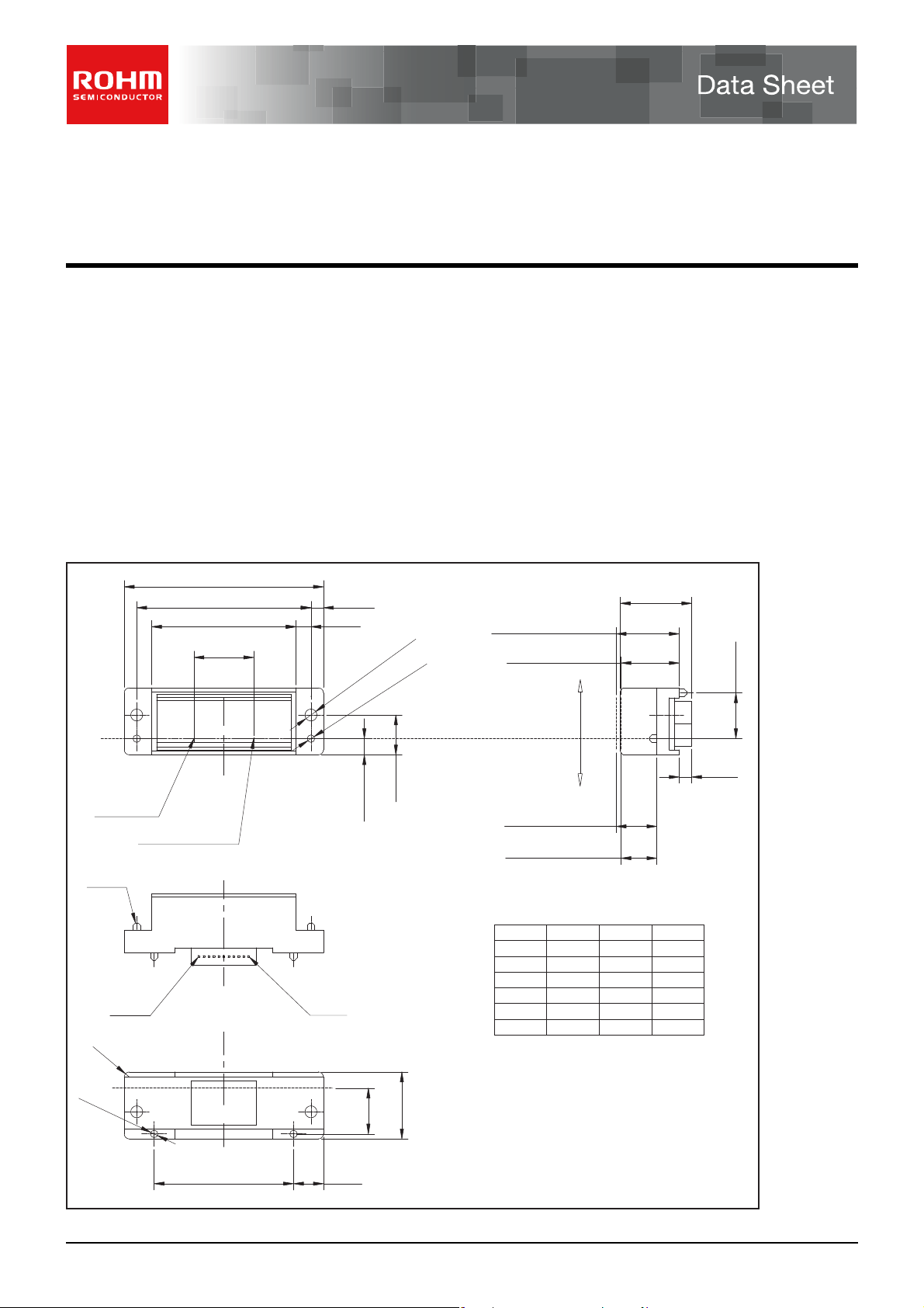
Dimensions (Unit : mm)
40±0.5
35
29
(Reading Width)
16.25
2.5
3
+0.1
0
0
2−φ2.4
-0.1
2−φ1.5
12.68 (Focus Point)
11.68 (Surface Level)
Max.15
9.2
No.130 Pixel
4−C0.5
4−R1
2−φ1.5
No.11
0
-0.1
No.1 Pixel
Scanning Line
8
3.25
No.1
13.45
9.2±0.5
14
6
8.18 (Focus Point)
7.18 (Surface Level)
Pin No. Pin No.Signal Signal
No.1
No.2
No.3
No.4
No.5
No.6
(NOTE 1) Deflection at the top of glass :
(NOTE 2) It is possible to design
(Connector No.)
Paper Feed Direction
GND
Ao
GND
GND
G-LED
V-LED
Housing : SHR-11V-S-B
Base : SM11B-SRSS-G-TB
No.7
No.8
No.9
No.10 GND
No.11 VDD
±0.2 tolerance.
CLK
SI
GND
(2.5)
±0.5
www.rohm.com
1/4
c
○
2011 ROHM Co., Ltd. All rights reserved.
2011.03 - Rev.B
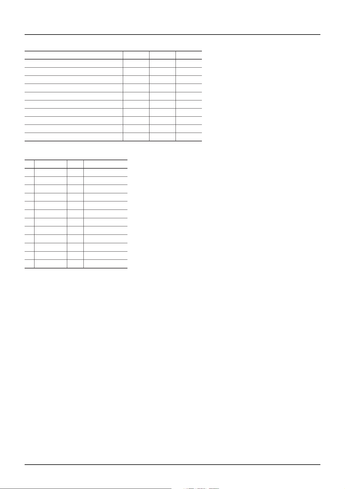
Characteristics
Parameter
Effective scanning width
Primary scan dot density
Total dot number
Power supply voltage
Scanning speed
Clock frequency
Minimum dynamic range
Operating temperature
Pin assignments
No.
Circuit
1
2
3
4
5
6
7
8ISP
11 IV
12 −NC
GND
Ao
GND
REF
R-GND
V-LED
CLK
DD
I / O
I
Ground
O
Analog Output
I
Ground
IV
Reference Voltage
I
LED ground
I
LED power supply
I
Clock
Start Pulse
Ground9IGND
Ground10 IGND
Power Supply
Functions
Symbol Typ. Unit
−
−
−
V
DD
SLT
CLK
−
16.25
200
128
3.3
0.1
8
1.0 VVRMax.Maximum dynamic range
0.5 VVRMin.
0.8±0.1
5 to 45
mm
dpi
dots
V
ms / line
MHz
VVodDark output
°C
Data Sheet LSH2001-AA10A
www.rohm.com
2/4
c
○
2011 ROHM Co., Ltd. All rights reserved.
2011.03 - Rev.B

Timing chart
(a) CLK Timing Chart
Data Sheet LSH2001-AA10A
1/fCLK
twCLK twCLK
50%
CLK
50%
SI
Ao
50% 50% 50%
50%
tHOLDtSETUP
1pixel 2pixel
ts
(b) Data Output Timing Chart
After turning on the SP pulse, the analog output shape starts from the setting up point of 65 clock pulse.
1 2 65 66 67 208
CLK
SP
Ao
Vref Output Period (64pixels)
1 to 64clock 1 to 144pixels
Note) Output blank part cannot be used as the analog output standard level.
Analog Output Period
www.rohm.com
3/4
c
○
2011 ROHM Co., Ltd. All rights reserved.
2011.03 - Rev.B

Data Sheet LSH2001-AA10A
Inner circuit
Peripheral circuit
V
GND
CLK
V
REF
V
LED
R
GND
SP
Ao
DD
1μF x 1
1
ANALOG MEMORY CIRCUIT
144
Contact Image Sensor Heads
562 118
R
C3
C4
R-GND
Ao
4
R3
C1
C5
V
DD
V
REF
∗ R1=R2=100Ω
R3=100kΩ
C1=C5=47μF
C2=100pF
C3=100μF, C4=0.1μF
Please adjust the value of resistance to fit your interface circuit.
7 1,3,9,10
C2
R1R2
SP CLK GNDVLED
www.rohm.com
4/4
c
○
2011 ROHM Co., Ltd. All rights reserved.
2011.03 - Rev.B

Notes
Notice
www.rohm.com
© 2011 ROHM Co., Ltd. All rights reserved.
Thank you for your accessing to ROHM product informations.
More detail product informations and catalogs are available, please contact us.
ROHM Customer Support System
http://www.rohm.com/contact/
R1120A
 Loading...