

ROHM LM358WPT Technical data
y
y
General-purpose Operational Amplifiers / Comparators
SIGNATURE SERIES
Operational Amplifiers
LM358DT/PT/ST/WDT/WPT,LM2904DT/PT/ST/WDT/WPT
LM324DT/PT/WDT,LM2902DT/PT/WDT
●Description
The Universal Standard family LM358 / 324, LM2904 /
2902 monolithic ICs integrate two independent
op-amps and phase compensation capacitors on a
single chip
and feature high-gain, low power consumption, and
an operating voltage range of 3[V] to 32[V]
(single power supply.)
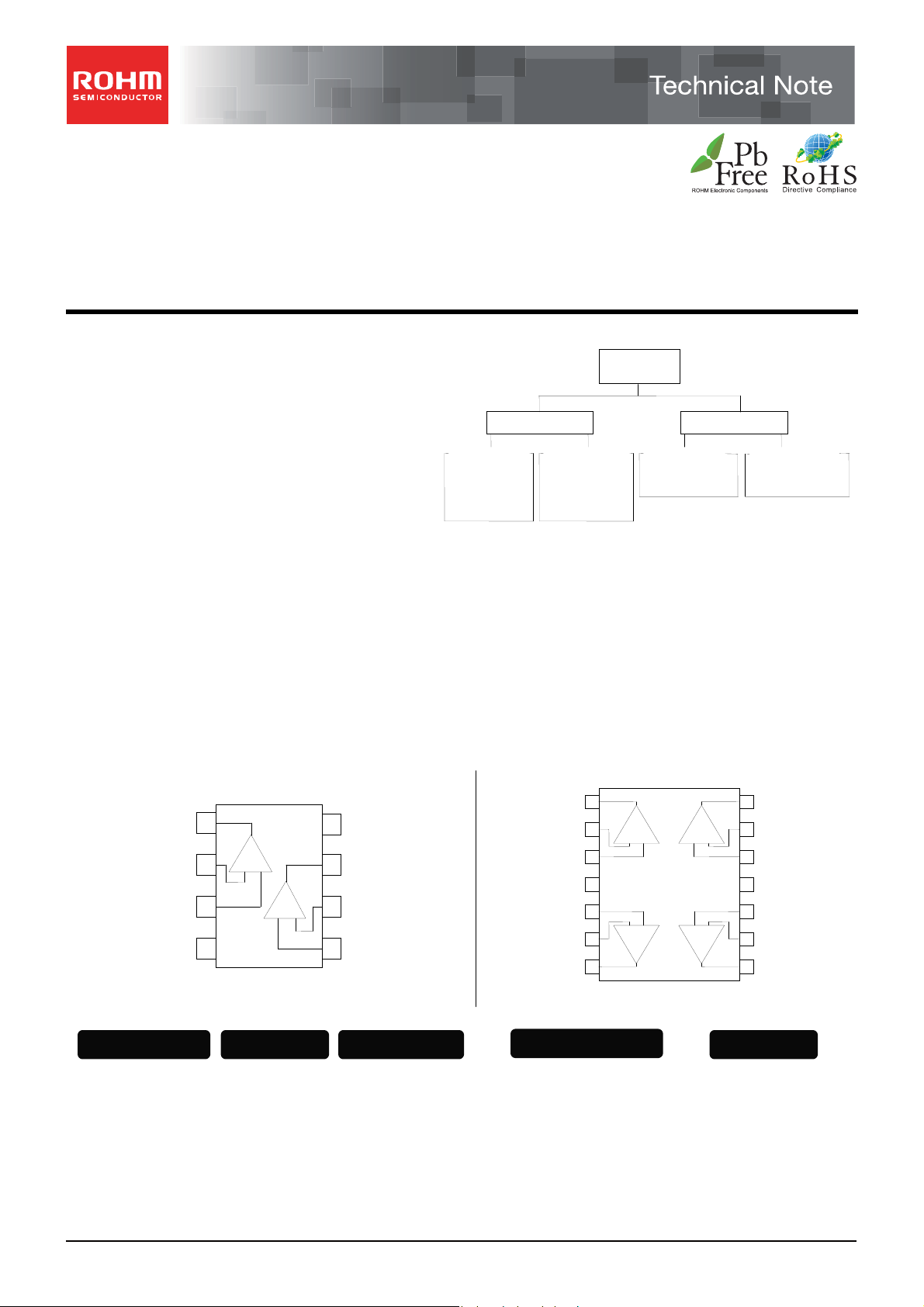
LM358 family LM324 family
LM358DT
LM358PT
LM358ST
LM358WDT
LM358WPT
●Features
1) Operating temperature range
Commercial Grade LM358/324 family :
Extended Industrial Grade LM2904/2902 family : -40[℃] to +125[℃]
2) Wide operating supply voltage
+3[V] to +32[V] (single supply)
±1.5[V] to ±16[V] (dual supply)
3) Low supply current
4) Common-mode input voltage range including ground
5) Differential input voltage range equal to maximum rated supply voltage
6) High large signal voltage gain
7) Wide output voltage range
●Pin Assignment
OUTPUT 1
INVERTING
INPUT 1
NON-INVERTING
INPUT 1
Vcc
1
2
-
+
3
-
4
+
-
+
Vcc
8
OUTPUT 2
7
INVERTING
6
INPUT 2
NON-INVERTING
5
INPUT 2
SO package8
LM358DT LM324PTLM358PT
LM358WDT
LM2904DT LM2904PT
LM2904WDT LM2904WPT
TSSOP8 TSSOP14
Mini SO8
LM358ST
LM358WPT LM2902PT
LM2904ST
Dual
0[℃] to + 70[℃]
OUTPUT 1
INVERTING
NON-INVERTING
NON-INVERTING
INVERTING
OUTPUT 2
SO package14
LM324DT
LM324WDT
LM2902DT
LM2902WDT
LM2904 famil
LM2904DT
LM2904PT
LM2904ST
LM2904WDT
LM2904WPT
INPUT 1
INPUT 1
+
Vcc
INPUT 2
INPUT 2
SIGNATURE
SERIES
1
2
- + + -
3
4
5
- + + -
6
7
LM324DT
LM324PT
LM324WDT
No.11094EBT05
Quad
LM2902 famil
LM2902DT
LM2902PT
LM2902WDT
14
OUTPUT 4
INVERTING
13
INPUT 4
NON-INVERTING
12
INPUT 4
Vcc
11
NON-INVERTING
10
INPUT 3
INVERTING
9
INPUT 3
8
OUTPUT 3
-
www.rohm.com
© 2011 ROHM Co., Ltd. All rights reserved.
1/17
2011.06 - Rev.B
LM358DT/PT/ST/WDT/WPT,LM2904DT/PT/ST/WDT/WPT
LM324DT/PT/WDT,LM2902DT/PT/WDT
Technical Note
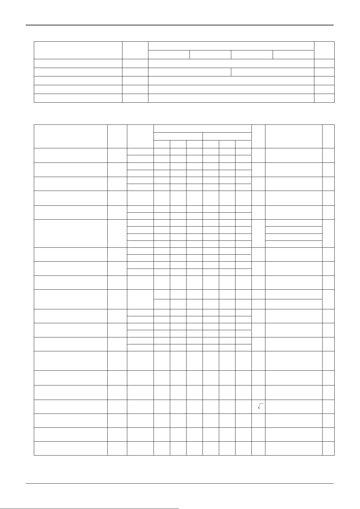
●Absolute Maximum Ratings (Ta=25[℃])
Parameter Symbol
LM358 family LM324 family LM2904 family LM2902 family
Rating
Supply Voltage VDD +32 V
Operating Temperature Range Topr 0 to +70 -40 to +125 ℃
Storage Temperature Range Tstg -65 to +150 ℃
Input Common-mode Voltage VICM -0.3 to +32 V
Maximum Junction Temperature Tjmax +150 ℃
●Electric Characteristics
○LM358,LM324 family(Unless otherwise specified, Vcc+=+5[V], Vcc-=0[V])
Parameter Symbol
Input Offset Voltage (*1) VIO
Input Offset Current (*1) IIO
Input Bias Current (*1) IIB
Large Signal Voltage Gain AVD 25℃ 25 100 - 25 100 - V/mV
Supply Voltage Rejection Ratio SVR
Supply Current (All Amp) ICC
Input Common-mode Voltage Range VICM
Common-mode Rejection Ratio CMR
Output Short Circuit Current (*2) Isource 25℃ 20 40 60 20 40 70 mA
Output Sink Current (*2) Isink 25℃
Output Voltage Swing Vopp
High Level Output Voltage VOH
Low Level Output Voltage
Slew Rate SR 25℃ - 0.6 - - 0.4 - V/μs
Gain Bandwidth Product GBP 25℃ - 1.1 - - 1.3 - MHz
Total Harmonic Distortion THD 25℃ - 0.02 - - 0.015 - %
Input Equivalent Noise Voltage en 25℃ - 55 - - 40 -
Temperature
range
25℃ - 2 7 - - 7
Full range - - 9 - - 9
25℃ - 2 30 - 2 30
Full range - - - - - 100
25℃ - 20 150 - 20 150
Full range - - 200 - - 300
25℃ 65 100 - 65 110 -
Full range 65 - - 65 - -
25℃ - - - - 0.7 1.2
25℃ - - - - 1.5 3 Vcc+=30[V],No Load
Full range - 0.7 1.2 - 0.8 3 Vcc+=5[V],No Load
Full range - - 2 - 1.5 3 Vcc+=30[V],No Load
25℃ - -
Full range - - Vcc+-2.0 - - Vcc+-2.0
25℃ 70 85 - 70 80 -
Full range 60 - - 60 - -
25℃ 0 - Vcc
Full range 0 - Vcc+-2.0 - - -
25℃ 27 28 - 27 28 -
Full range 27 - - 27 - -
VOL
25℃ - 5 20 - 5 20
Full range - - 20 - - 20
LM358 family LM324 family
Min. Typ. Max. Min. Typ. Max.
10 20 - 10 20 - mA
12 50 - 12 50 - μA
Limit
+
Vcc
-1.5 - - Vcc+-1.5
+
-1.5 - - -
Unit Conditions
VO=1.4[V],RS=0[Ω]
mV
5[V]< Vcc+<30[V]
0<VIC< Vcc
nA VO=1.4[V] 98
nA VO=1.4[V] 98
Vcc
VO=1.4[V] to 1 1.4[V]
RL=2[kΩ]
RS≦10[kΩ]
dB
Vcc
Vcc
mA
V Vcc+=30[V] 98
dB RS≦10[kΩ] 98
Vcc
VID=+1[V]
VO=+2[V],
Vcc
VO=+0.2[V],
Vcc
V RL=2[kΩ] 99
V Vcc+=30[V],RL=10[kΩ] 99
mV RL=10[kΩ] 99
RL=2[kΩ],CL=100[pF],
Vcc
VI=0.5[V] to 3[V],
Unity Gain
Vcc
CL=100[pF]
VIN=10[mV],f=100[kHz]
f=1[kHz],AV=20[dB]
RL=2[kΩ]
CL=100[pF],VO=2[Vpp]
f=1[kHz],RS=100[Ω]
HznV/
Vcc
+
-1.5[V]
+
=15[V]
+
=5[V] to 30[V]
+
=5[V],No Load
+
=15[V],VO=+2[V]
+
=15[V],VID=-1[V]
+
=15[V] ,VID=-1[V]
+
=15[V]
+
=30[V],RL=2[kΩ],
+
=30[V]
Unit
Fig.
No
98
98
98
99
99
99
99
99
99
99
Input Offset Voltage Drift DVIO - - 7 - - 7 - μV/℃ - -
Input Offset Current Drift DIIO - - 10 - - 10 - pA/℃ - -
Channel Separation VO1/VO2 25℃ - 120 - - 120 - dB 1[kHz]≦f≦20[kHz] 99
(*1) Absolute value
(*2) Under high temperatures, please consider the power dissipation when selecting the output current.
When output terminal is continuously shorted the output current reduces the internal temperature by flushing.
www.rohm.com
© 2011 ROHM Co., Ltd. All rights reserved.
2/17
2011.06 - Rev.B
LM358DT/PT/ST/WDT/WPT,LM2904DT/PT/ST/WDT/WPT
LM324DT/PT/WDT,LM2902DT/PT/WDT
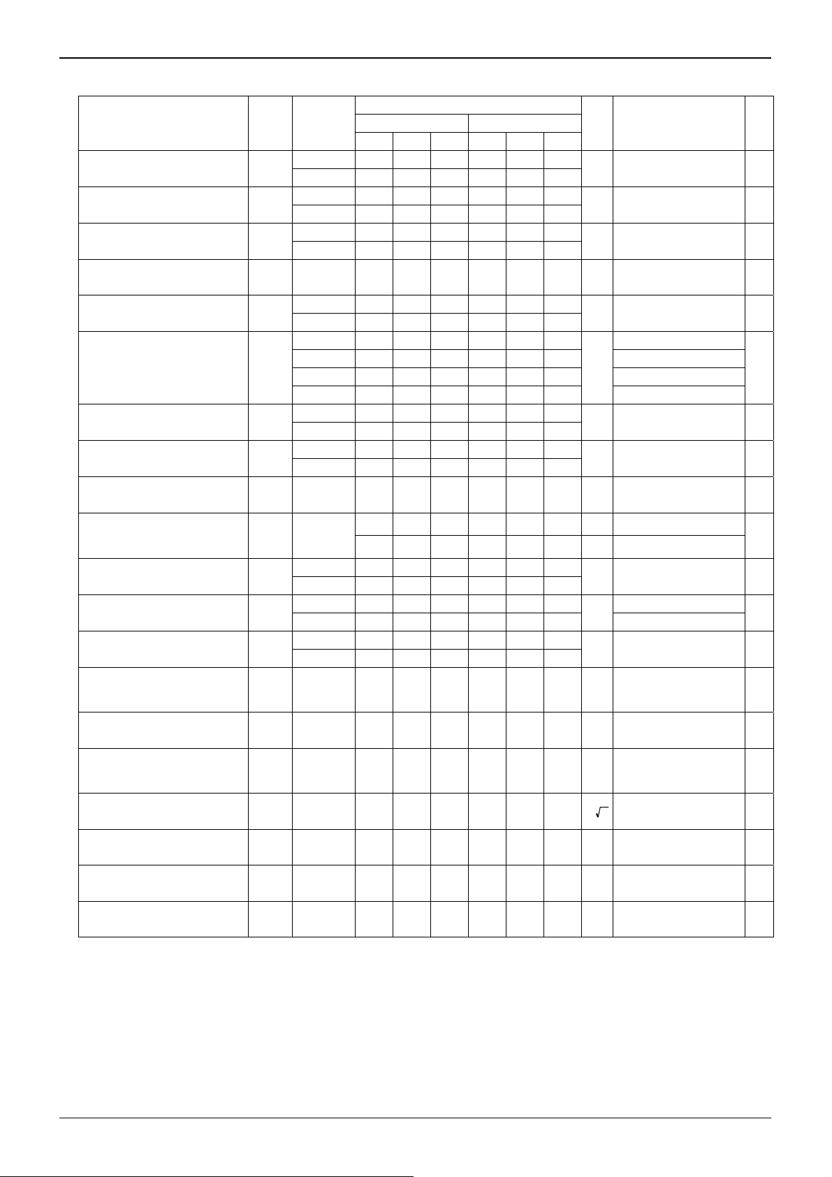
○LM2904,LM2902 family(Unless otherwise specified, Vcc+=+5[V], Vcc-=0[V])
Parameter Symbol
Temperature
range
LM2904 family LM2902 family
Min. Typ. Max. Min. Typ. Max.
Input Offset Voltage (*3) VIO
Input Offset Current (*3) IIO
Input Bias Current (*3) IIB
25℃ - 2 7 - 2 7
Full range - - 9 - - 9
25℃ - 2 50 - 2 30
Full range - - 200 - - 200
25℃ - 20 150 - 20 150
Full range - - 200 - - 300
Large Signal Voltage Gain AVD 25℃ 25 100 - 25 100 - V/mV
Supply Voltage Rejection Ratio SVR
25℃ 65 100 - 65 110 -
Full range 65 - - 65 - -
25℃ - 0.7 1.2 - 0.7 1.2
Supply Current (All Amp) ICC
25℃ - - - - 1.5 3 Vcc+=30[V],No Lord
Full range - - 2 - 0.8 1.2 Vcc+=5[V],No Lord
Full range - - - - 1.5 3 Vcc+=30[V],No Lord
Input Common-mode Voltage Range VICM
Common-mode Rejection Ratio CMR
25℃ - - Vcc
Full range - - Vcc+-2.0 - - Vcc+-2.0
25℃ 70 85 - 70 80 -
Full range 60 - - 60 - -
Output Short Circuit Current (*4) Isource 25℃ 20 40 60 20 40 70 mA
10 20 - 10 20 - mA
Output Sink Current (*4) Isink 25℃
12 50 - 12 50 - μA
Output Voltage Swing Vopp
High Level Output Voltage VOH
Low Level Output Voltage
VOL
25℃ 0 - Vcc
Full range 0 - Vcc+-2.0 - - -
25℃ 27 - - 27 28 -
Full range 27 28 - 27 - - Vcc+=30[V],RL=10[kΩ]
25℃ - 5 20 - 5 20
Full range - - 20 - - 20
Slew Rate SR 25℃ - 0.6 - - 0.4 - V/μs
Gain Bandwidth Product GBP 25℃ - 1.1 - - 1.3 - MHz
Total Harmonic Distortion THD 25℃ - 0.02 - - 0.015 - %
Input Equivalent Noise Voltage en 25℃ - - - - 40 -
Limit
+
-1.5 - - Vcc+-1.5
+
-1.5 - - -
Technical Note
Unit Conditions
mV VO=1.4[V] 98
nA VO=1.4[V] 98
nA VO=1.4[V] 98
+
Vcc
=15[V]
VO=1.4[V] to 1 1.4[V]
RL=2[kΩ]
dB RS≦10[kΩ] 99
+
Vcc
=5[V],No Lord
mA
+
V Vcc
dB RS=10[kΩ] 98
V RL=2[kΩ] 99
V
mV RL=10[kΩ] 99
=30[V] 98
+
Vcc
=+15[V],VO=+2[V]
VID=+1[V]
VO=2[V],Vcc
VID=-1[V]
VO=+0.2[V],
Vcc
Vcc
RL=2[kΩ],CL=100[pF],
Unity Gain
VI=0.5[V] to 3[V]
Vcc
Vcc
CL=100[pF]
VIN=10[mV]
+
=+5[V]
+
=+15[V] ,VID=-1[V]
+
=30[V],RL=10[kΩ]
+
=1.5[V]
+
=30[V],RL=2[kΩ]
f=1[kHz],AV=20[dB]
RL=2[kΩ]
CL=100[pF],
+
=30[V],VO=2[Vpp]
Vcc
f=1[kHz],RS=100[Ω]
+
HznV/
Vcc
=30[V]
Fig.
No
98
99
98
99
99
99
99
99
99
Input Offset Voltage Drift DVIO - - 7 - - 7 - μV/℃ - -
Input Offset Current Drift DIIO - - 10 - - 10 - pA/℃ - -
Channel Separation VO1/VO2 25℃ - 120 - - 120 - dB 1[kHz]≦f≦20[kHz] 99
(*3) Absolute value
(*4) Under high temperatures, please consider the power dissipation when selecting the output current.
When the output terminal is continuously shorted the output current reduces the internal temperature by flushing.
www.rohm.com
© 2011 ROHM Co., Ltd. All rights reserved.
3/17
2011.06 - Rev.B
LM358DT/PT/ST/WDT/WPT,LM2904DT/PT/ST/WDT/WPT
y
y
y
y
y
y
LM324DT/PT/WDT,LM2902DT/PT/WDT
Technical Note
●Reference Data LM358 family
800
600
LM358PT
LM358WPT
LM358ST
400
LM358 family
LM358DT
LM358WDT
0℃
LM358 famil
25℃
Fig. 1 Fig. 2 Fig. 3
200
POW ER DISSIPATION Pd [m W]
0
0 25 50 75 100
AMBIENT TEMPERATURE : Ta [℃]
Derating Curve
70
[℃]
LM358 family
70℃
Supply Current – Supply Voltage
LM358 famil
0℃
25℃
70℃
5V
3V
Supply Current – Ambient Temperature
0℃
25℃
70℃
Fig. 4 Fig. 5 Fig. 6
Maximum Output Voltage – Supply Voltage
(RL=10[kΩ])
3V
15V
5V
LM358 family
Maximum Output Voltage – Ambient Temperature
(VCC=5[V],RL=2[kΩ])
LM358 family LM358 famil
70℃
0℃
25℃
Output Source Current – Output Voltage
(VCC=5[V])
15V
3V
5V
Fig. 7 Fig. 8 Fig. 9
Output Source Current – Ambient Temperature
(VOUT=0[V])
LM358 famil
25℃
0℃
Output Sink Current – Output Voltage
(VCC=5[V])
32V
5V
LM358 famil
Output Sink Current – Ambient Temperature
(VOUT=VCC)
0℃
70℃
3V
70℃
Fig. 10 Fig. 11 Fig. 12
Low Level Sink Current - Supply Voltage
(*)The data above is ability value of sample, it is not guaranteed.
Low Level Sink Current - Ambient Temperature
(VOUT=0.2[V])
(VOUT=0.2[V])
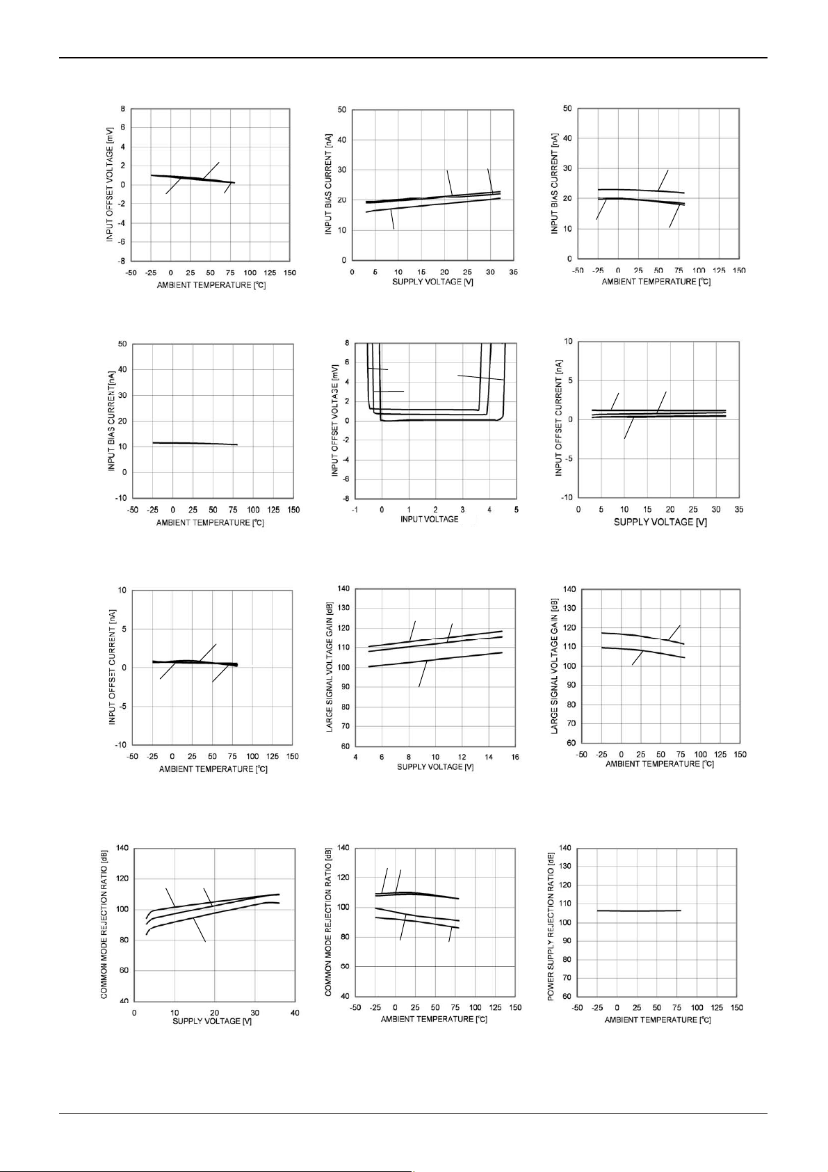
Input Offset Voltage - Supply Voltage
(Vicm=0[V], VOUT=1.4[V])
LM358 family
32V
LM358 family
LM358 famil
25℃
www.rohm.com
© 2011 ROHM Co., Ltd. All rights reserved.
4/17
2011.06 - Rev.B
LM358DT/PT/ST/WDT/WPT,LM2904DT/PT/ST/WDT/WPT
y
y
y
y
y
y
y
LM324DT/PT/WDT,LM2902DT/PT/WDT
Technical Note
●Reference Data LM358 family
LM358 family
LM358 family
5V
32V
3V
0℃
25℃
70℃
3V
Fig. 13 Fig. 14 Fig. 15
Input Offset Voltage – Ambient Temperature
(Vicm=0[V], VOUT=1.4[V])
Input Bias Current – Supply Voltage
(Vicm=0[V], VOUT=1.4[V])
LM358 family
Input Bias Current – Ambient Temperature
(Vicm=0[V],VOUT=1.4[V])
LM358 famil
25℃
70℃
0℃
0℃
70℃
Fig. 16 Fig. 17 Fig. 18
Input Bias Current – Ambient Temperature
(VCC=30[V],Vicm=28[V],VOUT=1.4[V])
Input Offset Voltage – Common Mode Input Voltage
LM358 famil
(VCC=5[V])
Input Offset Current – Supply Voltage
(Vicm=0[V],VOUT=1.4[V])
LM358 famil
3V
0℃
25℃
5V
32V
70℃
5V
Fig. 19 Fig. 20 Fig. 21
Input Offset Current
– Ambient Temperature
(Vicm=0[V],VOUT=1.4[V])
0℃
Large Signal Voltage Gain
LM358 famil
36V
25℃
– Supply Voltage
(RL=2[kΩ])
32V
Large Signal Voltage Gain
– Ambient Temperature
(RL=2[kΩ])
LM358 family
70℃
5V
3V
Fig. 22 Fig. 23 Fig. 24
(*)The data above is ability value of sample, it is not guaranteed.
Common Mode Rejection Ratio
– Supply Voltage
Common Mode Rejection Ratio
– Ambient Temperature
Power Supply Rejection Ratio
– Ambient Temperature
25℃
5V
32V
15V
LM358 famil
LM358 famil
LM358 family
LM358 famil
www.rohm.com
© 2011 ROHM Co., Ltd. All rights reserved.
5/17
2011.06 - Rev.B

LM358DT/PT/ST/WDT/WPT,LM2904DT/PT/ST/WDT/WPT
y
y
y
y
y
y
LM324DT/PT/WDT,LM2902DT/PT/WDT
Technical Note
●Reference Data LM324 family
LM324 family
1000
LM324ST
800
LM324 family
LM324DT
LM324WDT
Fig. 25 Fig. 26 Fig. 27
600
400
200
POWER DISSIPATION Pd [mW]
0
0 25 50 75 100
AM B IEN T TEMP E RA TU R E : Ta [℃ ]
Derating Curve
70
[℃]
LM324 family
0℃
70℃
Supply Current – Supply Voltage
0℃
25℃
BA2904 family
25℃
5V
Supply Current – Ambient Temperature
LM324 famil
0℃
25℃
70℃
70℃
Fig. 28 Fig. 29 Fig. 30
Maximum Output Voltage – Supply Voltage
(RL=10[kΩ])
3V
15V
5V
LM324 family
Maximum Output Voltage – Ambient Temperature
(VCC=5[V],RL=2[kΩ])
LM324 family LM324 family
70℃
0℃
25℃
Output Source Current – Output Voltage
(VCC=5[V])
15V
5V
Fig. 31 Fig. 32 Fig. 33
Output Source Current – Ambient Temperature
(VOUT=0[V])
25℃
LM324 famil
0℃
Output Sink Current – Output Voltage
(VCC=5[V])
32V
5V
LM324 famil
Output Sink Current – Ambient Temperature
(VOUT=VCC)
0℃
70℃
3V
70℃
Fig. 34 Fig. 35 Fig. 36
Low Level Sink Current - Supply Voltage
(*)The data above is ability value of sample, it is not guaranteed.
Low Level Sink Current - Ambient Temperature
(VOUT=0.2[V])
(VOUT=0.2[V])
Input Offset Voltage - Supply Voltage
(Vicm=0[V], VOUT=1.4[V])
32V
3V
3V
25℃
LM324 famil
BA2904 family
LM324 famil
LM324 famil
www.rohm.com
© 2011 ROHM Co., Ltd. All rights reserved.
6/17
2011.06 - Rev.B
 Loading...