

Page 1

查询EMF6供应商
Transistors
Power management (dual transistors)
EMF6
2SA2018 and 2SK3019 are housed independently in a EMT6 package.
EMF6
!!!!Application
Power management circuit
!!!!Features
1) Power switching circuit in a single package.
2) Mounting cost and area can be cut in half.
!!!!Structure
Silicon epitaxial planar transistor
!!!!Equivalent circuits
(1)(2)(3)
Tr2
(4) (5) (6)
Tr1
!!!!External dimensions (Units : mm)
(3)
ROHM : EMT6
Abbreviated symbol:F6
0.22
0.13
(4)
(6)
0.5
1.0
(2)(5)
(1)
1.2
1.6
1.6
0.5
0.5
Each lead has
same dimensions
!!!!Packaging specifications
Type
Package
Marking
Code
Basic ordering unit (pieces)
EMF6
EMT6
F6
T2R
8000
1/5
Page 2

Transistors
!!!!Absolute maximum ratings (Ta=25°C)
Tr1
Parameter Symbol
CBO
Collector-base voltage
Collector-emitter voltage
Emitter-base voltage
Collector current
Power dissipation
Junction temperature
Range of storage temperature
∗1 Single pulse PW=1ms
∗2 120mW per element must not be exceeded. Each terminal mounted on a recommended land.
V
V
CEO
V
EBO
I
I
CP
P
Tj
Tstg
C
C
Limits
−15
−12
−6
−500
−1.0
150(TOTAL)
150
−55~+150
Tr2
Parameter
Drain-source voltage
Gate-source voltage
Drain current
Reverse drain
current
Continuous
Pulsed
Continuous
Pulsed
Total power dissipation
Channel temperature
Range of storage temperature
∗1 PW≤10ms Duty cycle≤50%
∗2 120mW per element must not be exceeded. Each terminal mounted on a recommended land.
Symbol
DSS
V
V
GSS
I
D
DP
I
I
DR
I
DRP
P
Tch
Tstg
D
Limits
30
±20
100
200 mA
100 mA
200
150(TOTAL)
150
−55~+150
Unit
V
V
V
mA
A
mW
°C
°C
Unit
V
V
mA
mA
mW
°C
°C
∗1
∗2
∗1
∗1
∗2
EMF6
!!!!
Electrical characteristics
(Ta=25°C)
Tr1
Parameter Symbol Min. Typ. Max. Unit Conditions
Collector-emitter breakdown voltage
Collector-base breakdown voltage
Emitter-base breakdown voltage
Collector cut-off current
Emitter cut-off current
Collector-emitter saturation voltage
DC current gain
Transition frequency
Collector output capacitance
Tr2
Parameter
Gate-source leakage
Drain-source breakdown voltage
Zero gate voltage drain current
Gate-threshold voltage
Static drain-source
on-state resistance
Forward transfer admittance
Input capacitance
Output capacitance
Reverce transfer capacitance
Turn-on delay time
Rise time
Turn-off delay time
Fall time
BV
BV
BV
I
I
V
CE(sat)
CBO
EBO
h
f
CEO
CBO
EBO
FE
T
−12
−15
−6
−−
−−
−−
−−
−−
−−100
270 − 680
260
−
Cob − 6.5 −
Symbol
GSS
I
(BR)DSS
V
DSS
I
V
GS(th)
DS(on)
R
|Y
fs
C
iss
C
oss
C
rss
t
d(on)
r
t
t
d(off)
f
t
Min. Typ. Max. Unit Conditions
−−
30
−−
−−
0.8
|
20
−
58Ω
−
713Ω
−
−−ms V
13
−
9
−
4
−
15
−
35
−
80
−
80
−
−100
−100
nA VCB=−15V
nA VEB=−6V
−250 mV
MHz
−
pF
±1 µA
1.0 µA
1.5
pF
−
− pF
− pF
− ns
ns
−
− ns
− ns
V
C
=−1mA
I
V
I
C
=−10µA
V
E
=−10µA
I
IC=−200mA, IB=−10mA
CE
− V
=−2V, IC=−10mA
VCE=−2V, IE=10mA, f=100MHz
V
CB
=−10V, IE=0mA, f=1MHz
VGS=±20V, VDS=0V
V
I
D
=10µA, VGS=0V
VDS=30V, VGS=0V
DS
VV
=3V, ID=100µA
ID=10mA, VGS=4V
D
=1mA, VGS=2.5V
I
DS
=3V, ID=10mA
V
DS
=5V, VGS=0V, f=1MHz
D
=10mA, VDD 5V,
I
GS
=5V, RL=500Ω,
V
GS
=10Ω
R
2/5
Page 3

Transistors
!!!!Electrical characteristic curves
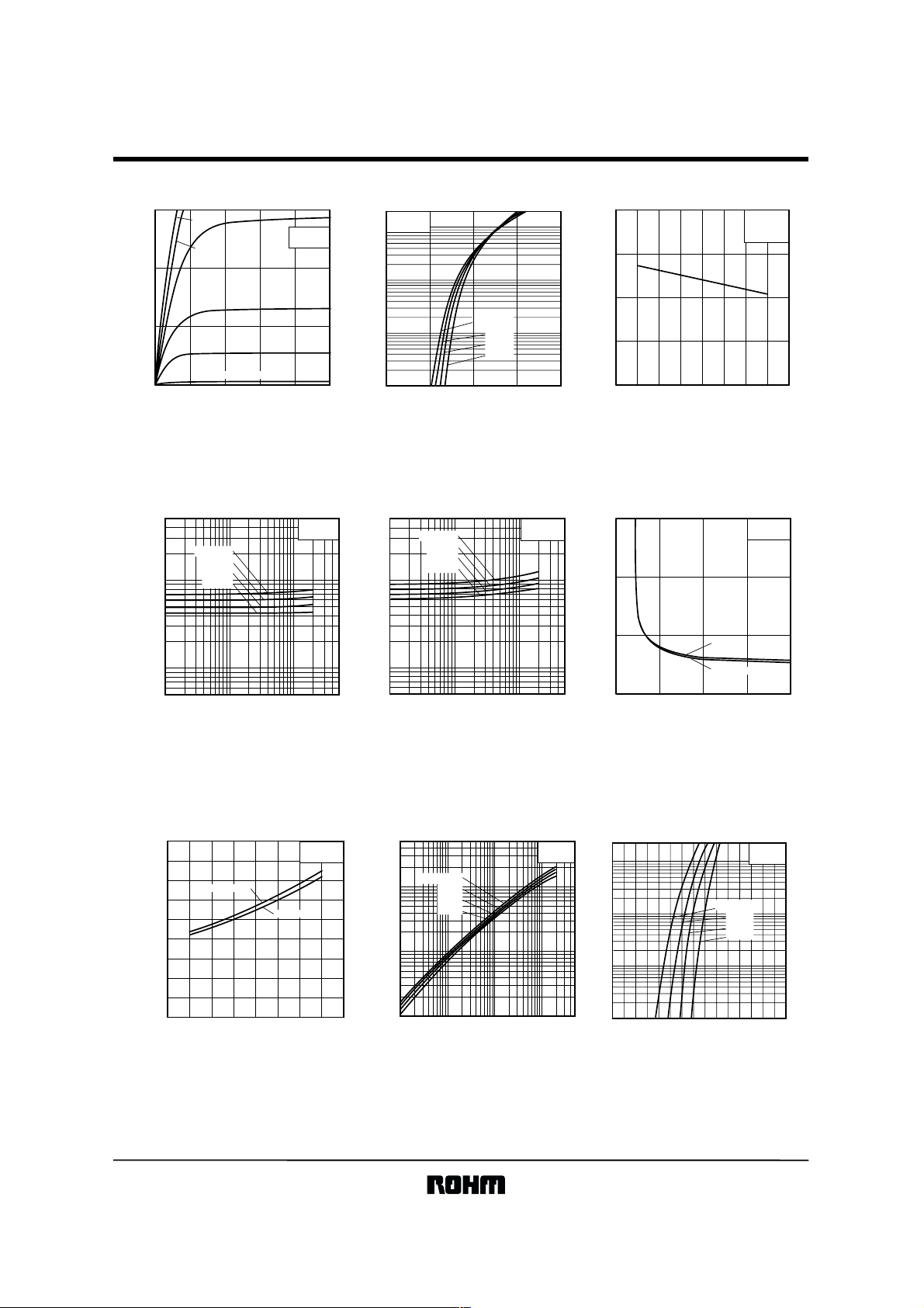
Tr1
1000
VCE=2V
Pulsed
(mA)
C
100
10
COLLECTOR CURRENT : I
1
0
Fig.1 Grounded emitter propagation
Ta=125°C
Ta=25°C
Ta= −40°C
BASE TO EMITTER VOLTAGE : V
characteristics
BE
1.41.0 1.20.4 0.6 0.80.2
(V)
1000
FE
100
10
DC CURRENT GAIN : h
1
1 10 100 1000
Ta=125°C
Ta=25°C
Ta=−40°C
COLLECTOR CURRENT : I
C
Fig.2 DC current gain vs.
collector current
(mA)
VCE=2V
Pulsed
EMF6
1000
Ta=25°C
(mV)
Pulsed
CE(sat)
100
IC/IB=50
IC/IB=20
IC/IB=10
10
1
1 10 100 1000
C
COLLECTOR CURRENT : I
COLLECTOR SATURATION VOLTAGE : V
(mA)
Fig.3 Collector-emitter saturation voltage
vs. collector current ( Ι )
1000
(V)
IC/IB=20
Pulsed
CE (sat)
Ta=25°C
Ta=125°C
Ta=−40°C
C
(mA)
100
10
1
1 10 100 1000
COLLECTOR CURRENT : I
COLLECTOR SATURATION VOLTAGE : V
Fig.4 Collector-emitter saturation voltage
vs. collector current ( ΙΙ )
1000
100
10
Cib
Cob
I
E
=
0A
f=1MHz
Ta=25°C
10000
(mV)
BE (sat)
1000
100
10
1 10 100 1000
BASER SATURATION VOLTAGE : V
Ta=25°C
COLLECTOR CURRENT : I
Ta=−40°C
Ta=125°C
Fig.5 Base-emitter saturation voltage
vs. collector current
IC/IB=20
Pulsed
C
(mA)
1000
VCE=2V
Ta=25°C
Pulsed
(MHz)
T
100
10
TRANSITION FREQUENCY : f
1
1 10 100 1000
EMITTER CURRENT : I
Fig.6 Gain bandwidth product
vs. emitter current
E
(mA)
1
EMITTER INPUT CAPACITANCE : Cib (pF)
COLLECTOR OUTPUT CAPACITANCE : Cob (pF)
EMITTER TO BASE VOLTAGE : V
Fig.7 Collector output capacitance
1 10 1000.1
vs. collector-base voltage
Emitter input capacitance
vs. emitter-base voltage
EB
V)
(
3/5
Page 4
Transistors
Tr2
0.15
(A)
D
0.1
0.05
DRAIN CURRENT : I
4V
0
012345
DRAIN-SOURCE VOLTAGE : VDS (V)
3V
3.5V
2.5V
2V
VGS=1.5V
Fig.9 Typical output characteristics
Ta=25°C
Pulsed
200m
V
DS
=3V
100m
Pulsed
50m
(A)
D
20m
10m
5m
2m
1m
0.5m
DRAIN CURRENT : I
0.2m
0.1m
04
1
GATE-SOURCE VOLTAGE : VGS (V)
Ta=125°C
75°C
25°C
−25°C
2
Fig.10 Typical transfer characteristics
EMF6
2
(V)
GS(th)
1.5
1
0.5
GATE THRESHOLD VOLTAGE : V
0
−25 25 50 75 100 125 150
3
−50 0
CHANNEL TEMPERATURE : Tch (°C)
Fig.11 Gate threshold voltage vs.
channel temperature
VDS
I
D
=0.1mA
Pulsed
=3V
50
(Ω)
DS(on)
STATIC DRAIN-SOURCE
ON-STATE RESISTANCE : R
Ta=125°C
20
10
0.5
0.001
5
2
1
75°C
25°C
−25°C
0.002 0.005 0.01 0.02 0.05 0.1 0.2 0.5
DRAIN CURRENT : ID (A)
V
Pulsed
Fig.12 Static drain-source on-state
resistance vs. drain current ( Ι )
9
8
(Ω)
7
DS(on)
6
5
4
3
2
1
STATIC DRAIN-SOURCE
ON-STATE RESISTANCE : R
0
−50 0 25 150
ID=100mA
ID=50mA
−25 50 75 100 125
CHANNEL TEMPERATURE : Tch (°C)
GS
=4V
VGS=4V
Pulsed
50
Ta=125°C
(Ω)
20
DS(on)
10
5
2
1
STATIC DRAIN-SOURCE
ON-STATE RESISTANCE : R
0.5
0.001
75°C
25°C
−25°C
0.002 0.005 0.01 0.02 0.05 0.1 0.2 0.5
DRAIN CURRENT : ID (A)
V
Pulsed
Fig.13 Static drain-source on-state
resistance vs. drain current ( ΙΙ )
0.5
0.2
Ta=−25°C
0.1
0.05
0.02
0.01
0.005
FORWARD TRANSFER
ADMITTANCE : |Yfs| (S)
0.002
0.001
25°C
75°C
125°C
0.0001
0.0002 0.0005 0.001 0.002 0.005 0.01 0.02 0.05
DRAIN CURRENT : ID (A)
GS
=2.5V
V
DS
=3V
Pulsed
0.1 0.2 0.5
15
(Ω)
DS(on)
10
5
STATIC DRAIN-SOURCE
ON-STATE RESISTANCE : R
0
0 5 10 15 20
GATE-SOURCE VOLTAGE : VGS (V)
ID=0.1A
ID=0.05A
Fig.14 Static drain-source on-state
resistance vs. gate-source
voltage
200m
(A)
100m
DR
50m
20m
10m
5m
2m
1m
0.5m
REVERSE DRAIN CURRENT : I
0.2m
0.1m
SOURCE-DRAIN VOLTAGE : VSD (V)
Ta=125°C
75°C
25°C
−25°C
Ta=25°C
Pulsed
V
GS
=0V
Pulsed
1.510.50
Fig.15 Static drain-source on-state
resistance vs. channel temperature
Fig.16 Forward transfer admittance vs.
drain current
Fig.17 Reverse drain current vs.
source-drain voltage ( Ι )
4/5
Page 5

Transistors
EMF6
200m
(A)
100m
DR
50m
20m
10m
V
GS
=4V
5m
2m
1m
0.5m
REVERSE DRAIN CURRENT : I
0.2m
0.1m
SOURCE-DRAIN VOLTAGE : VSD (V)
0V
Fig.18 Reverse drain current vs.
source-drain voltage ( ΙΙ )
Ta=25°C
Pulsed
CAPACITANCE : C (pF)
1.510.50
50
20
10
5
2
1
0.5
0.1
0.2 0.5 1 2 5 10 20 50
DRAIN-SOURCE VOLTAGE : VDS (V)
Fig.19 Typical capacitance vs.
drain-source voltage
Ta=25°C
f=1MH
VGS=0V
C
iss
C
oss
C
rss
Z
SWITHING TIME : t (ns)
1000
500
200
100
50
20
10
5
2
0.1
t
f
t
d(off)
t
r
t
d(on)
0.2 0.5 1 2 5 10 20 50
DRAIN CURRENT : ID (mA)
Fig.20 Switching characteristics
Ta=25°C
DD
=5V
V
GS
=5V
V
G
=10Ω
R
Pulsed
100
5/5
 Loading...