

Page 1
Datasheet
www.rohm.com
© 2012 ROHM Co., Ltd. All rights reserved.
DTA044E series
PNP -100mA -50V Digital Transistors (Bias Resistor Built-in Transistors)
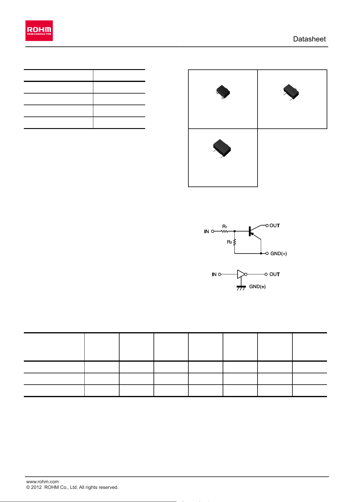
l
Outline
l
Features
1) Built-In Biasing Resistors, R1 = R2 = 47kW.
2) Built-in bias resistors enable the configuration of
an inverter circuit without connecting external
input resistors (see inner circuit).
3) The bias resistors consist of thin-film resistors
with complete isolation to allow negative biasing
of the input. They also have the advantage of
l
Inner circuit
completely eliminating parasitic effects.
4) Only the on/off conditions need to be set for
operation, making the circuit design easy.
5) Complementary NPN Types :DTC044E series
6) Lead Free/RoHS Compliant.
l
Application
Switching circuit, Inverter circuit, Interface circuit,
Driver circuit
l
Packaging specifications
R
1
47kW
R
2
47kW
Parameter
Value
V
CC
-50V
I
C(MAX.)
-100mA
Part No.
Package
Package
size
(mm)
Taping
code
8,000318
Tape width
(mm)
Basic
ordering
unit (pcs)
Marking
Reel size
(mm)
DTA044EM
VMT3
1212
T2L
180
3,000
31
DTA044EUB
3,000
31
DTA044EEB
EMT3F
1616
TL
180
8
UMT3F
2021
TL
180
8
VMT3
EMT3F
UMT3F
DTA044EM
(SC-105AA)
OUT
IN
GND
OUT
IN
GND
DTA044EUB
(SC-85)
DTA044EEB
(SC-89)
OUT
IN
GND
1/7
2012.05 - Rev.B
Page 2
www.rohm.com
© 2012 ROHM Co., Ltd. All rights reserved.
Data Sheet
DTA044E series
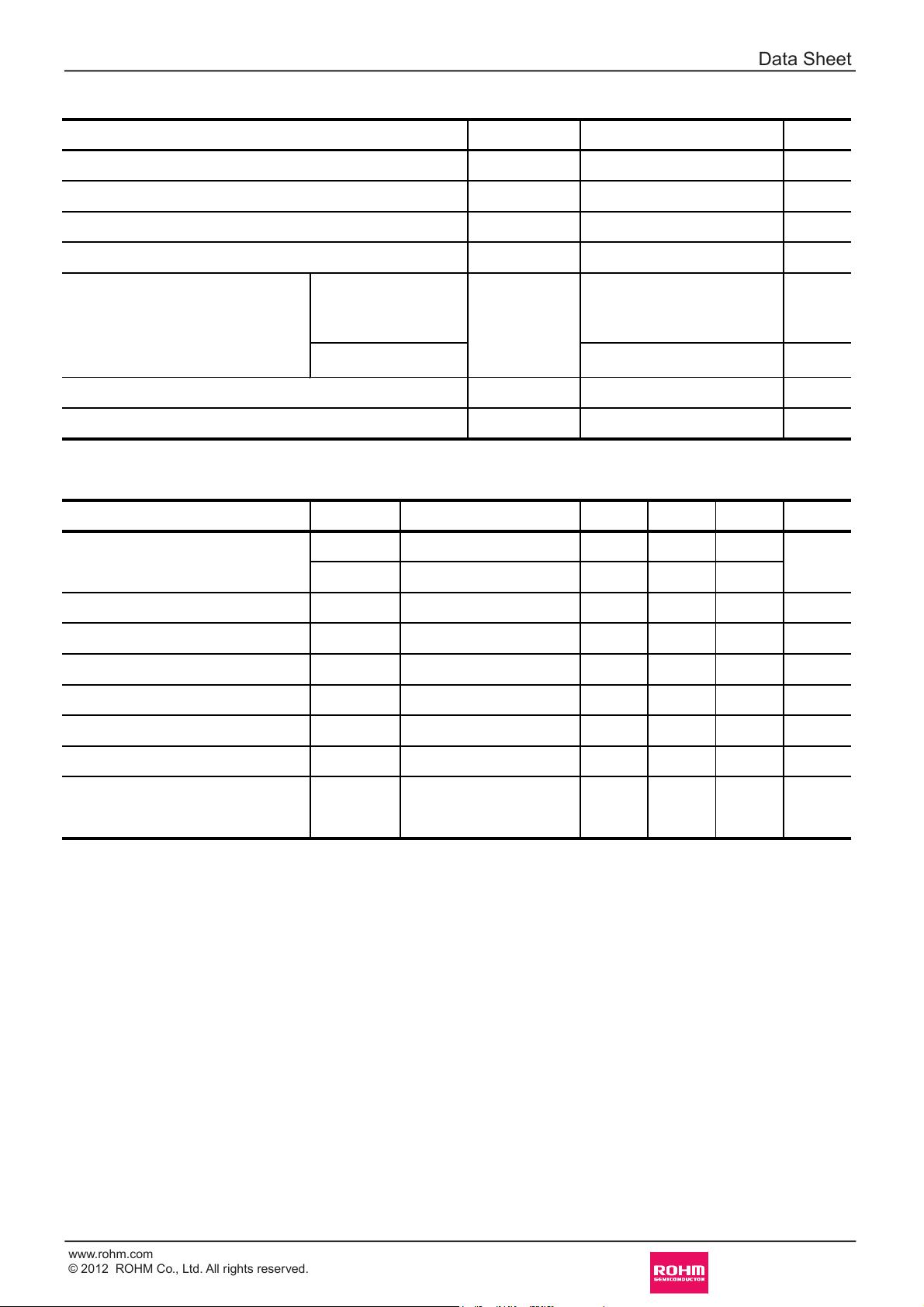
lAbsolute maximum ratings (Ta = 25°C)
Supply voltage
Input voltage
Output current
Collector current
Power dissipation
Junction temperature
Range of storage temperature
lElectrical characteristics(Ta = 25°C)
*1 Characteristics of built-in transistor
*2 Each terminal mounted on a reference footprint
Parameter
Symbol
Values
Unit
V
CC
-50
V
V
IN
-40 to +10
V
I
O
-30
mA
I
C(MAX.)
*1
-100
mA
P
D
*2
DTA044EUB
200
mW
150
mW
DTA044EM
DTA044EEB
T
j
150
°C
T
stg
-55 to +150
°C
Parameter
Symbol
Conditions
Unit
Min.
Typ.
Max.
Input voltage
V
I(off)
V
CC
= -5V, IO = -0.1mA
-
-
V
V
I(on)
VO = -0.3V, IO = -2mA
-3.0
-
-
-0.8
V
Input current
I
I
VI = -5V
-
-
-0.18
mA
Output voltage
V
O(on)
IO / II = -5mA / -0.5mA
-
-0.07
-0.15
mA
DC current gain
G
I
VO = -10V, IO = -5mA
80--
-
Output current
I
O(off)
V
CC
= -50V, VI = 0V
-
-
-0.5
kW
Resistance ratio
R2/R
1
-
0.811.2
-
Input resistance
R
1
-
32.9
47
61.1
MHz
Transition frequency
fT
*1
V
CE
= -10V, IE = 5mA,
f = 100MHz
-
250
-
2/7
2012.05 - Rev.B
Page 3
www.rohm.com
© 2012 ROHM Co., Ltd. All rights reserved.
Data Sheet
DTA044E series
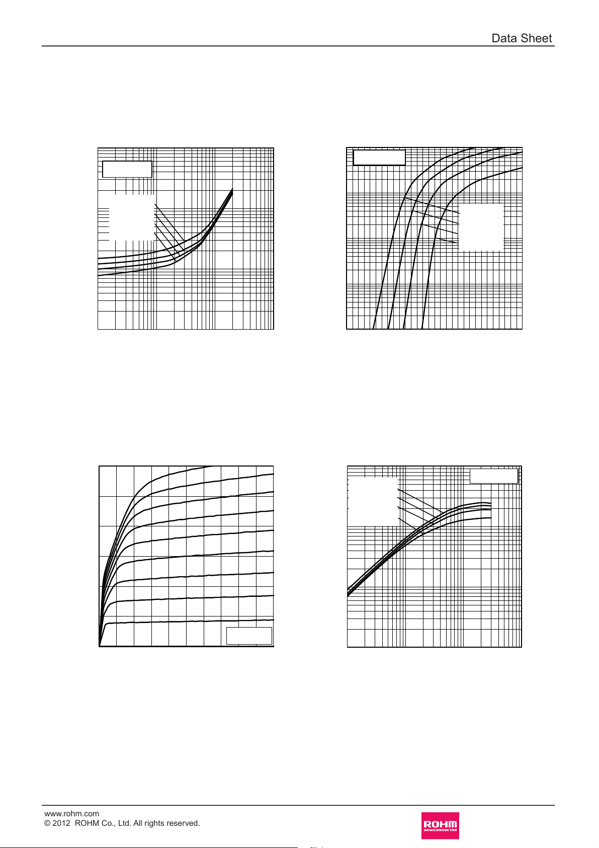
lElectrical characteristic curves(Ta = 25°C)
-0.1
-1
-10
-100
-0.1 -1 -10 -100
VO= -0.3V
Ta= -40ºC
Ta=25ºC
Ta=75ºC
Ta=125ºC
-0.001
-0.01
-0.1
-1
-10
0 -0.5 -1 -1.5 -2 -2.5 -3
Ta=125ºC
Ta=75ºC
Ta=25ºC
Ta= -40ºC
VCC= -5.0V
0
-10
-20
-30
0 -5 -10
-100μA
0A
-120μA
-140μA
-160μA
-180μA
-200μA
-40μA
-60μA
-80μA
II=
Ta=25ºC
1
10
100
1000
-0.1 -1 -10 -100
Ta=125ºC
Ta=75ºC
Ta=25ºC
Ta= -40ºC
VO= -10V
Fig.1 Input voltage vs. output current
(ON characteristics)
INPUT VOLTAGE : V
I(on)
[V]
OUTPUT CURRENT : IO [mA]
Fig.2 Output current vs. input voltage
(OFF characteristics)
OUTPUT CURRENT : I
O
[mA]
INPUT VOLTAGE : V
I(off)
[V]
Fig.3 Output current vs. output voltage
OUTPUT CURRENT : I
O
[mA]
OUTPUT VOLTAGE : VO [V]
Fig.4 DC current gain vs. output current
DC CURRENT GAIN : G
I
OUTPUT CURRENT : IO [mA]
3/7
2012.05 - Rev.B
Page 4

www.rohm.com
© 2012 ROHM Co., Ltd. All rights reserved.
Data Sheet
DTA044E series
lElectrical characteristic curves(Ta = 25°C)
-0.001
-0.01
-0.1
-1
-0.1 -1 -10 -100
IO/II=10
Ta=125ºC
Ta=75ºC
Ta=25ºC
Ta= -40ºC
Fig.5 Output voltage vs. output current
OUTPUT VOLTAGE : V
O(on)
[V]
OUTPUT CURRENT : IO [mA]
4/7
2012.05 - Rev.B
Page 5

www.rohm.com
© 2012 ROHM Co., Ltd. All rights reserved.
Data Sheet
DTA044E series
lDimensions (Unit : mm)
Dimension in mm/inches
VMT3
Patterm of terminal position areas
b1
D
e b
E
H
x S A
A
c
L
Lp
A1
A
S
e1
l1
b2
b3
l1
e
MIN MAX MIN MAX
A 0.45 0.55 0.018 0.022
A1 0.00 0.10 0 0.004
b 0.17 0.27 0.007 0.011
b1 0.27 0.37 0.011 0.015
c 0.08 0.18 0.003 0.007
D 1.10 1.30 0.043 0.051
E 0.70 0 .90 0.028 0.035
e
HE 1.10 1.30 0.043 0.051
L 0.10 0.30 0.004 -
Lp 0.20 0.40 0.008 -
x - 0.10 - 0.004
MIN MAX MIN MAX
e1
b2 - 0.37 - 0.015
b3 - 0.47 - 0.019
l1 - 0.50 - 0.02
DIM
MILIMETERS
INCHES
0.80
0.03
DIM
MILIMETERS
INCHES
0.40
0.02
5/7
2012.05 - Rev.B
Page 6

www.rohm.com
© 2012 ROHM Co., Ltd. All rights reserved.
Data Sheet
DTA044E series
lDimensions (Unit : mm)
Dimension in mm/inches
EMT3F
Patterm of terminal position areas
D
e
E
E
H
A
b
x S A
L
c
Lp
A2A1
S
e1
e
b2
l1
A
MIN MAX MIN MAX
A 0.65 0.85
A1 0.00 0.10 0 0.004
A2 0.60 0.80 0.024 0.031
b 0.21 0.36 0.008 0.0 14
c 0.08 0.18 0.003 0.007
D 1.50 1.70 0.059 0.067
E 0.76 0.96 0.03 0.038
e
HE 1.50 1.70 0.059 0.067
L
Lp 0.35 0.55 0.014 0.022
x - 0.10 - 0.004
MIN MAX MIN MAX
e1 - 1.05 - 0.041
b2 - 0.46 - 0.018
l1 - 0.65 - 0.026
DIM
0.50
0.02
0.37
0.015
MILIMETERS
INCHES
DIM
MILIMETERS
INCHES
6/7
2012.05 - Rev.B
Page 7

www.rohm.com
© 2012 ROHM Co., Ltd. All rights reserved.
Data Sheet
DTA044E series
lDimensions (Unit : mm)
Dimension in mm/inches
UMT3F
Patterm of terminal position areas
D
E
H
b
e
x S A
c
L
Lp
A1 A2
S
e1
e
l1
b2
E
A
A
MIN MAX MIN MAX
A 0.85 1.05 0.033 0.041
A1 0.00 0.10 0 0.004
A2 0.80 1.00 0.031 0.039
b 0.27 0.42 0.01 1 0.017
c 0.08 0.18 0.003 0.007
D 1.90 2.10 0.075 0.083
E 1.15 1.35 0.045 0.053
e
HE 2.00 2.20 0.079 0.087
L
Lp 0.43 0.63 0.017 0.025
x - 0.10 - 0.004
MIN MAX MIN MAX
e1
b2 - 0.52 - 0.02
l1 - 0.83 - 0.033
INCHES
0.65
0.03
0.02
DIM
MILIMETERS
0.425
DIM
MILIMETERS
INCHES
1.47
0.058
7/7
2012.05 - Rev.B
Page 8

Notes
No copying or reproduction of this document, in par t or in whole, is permitted without the
consent of ROHM Co.,Ltd.
The content specied herein is subject to change for improvement without notice.
The content specied herein is for the purpose of introducing ROHM's products (hereinafter
"Products"). If you wish to use any such Product, please be sure to refer to the specications,
which can be obtained from ROHM upon request.
Examples of application circuits, circuit constants and any other information contained herein
illustrate the standard usage and operations of the Products. The peripheral conditions must
be taken into account when designing circuits for mass production.
Great care was taken in ensuring the accuracy of the information specied in this document.
However, should you incur any damage arising from any inaccuracy or misprint of such
information, ROHM shall bear no responsibility for such damage.
The technical information specied herein is intended only to show the typical functions of and
examples of application circuits for the Products. ROHM does not grant you, explicitly or
implicitly, any license to use or exercise intellectual property or other rights held by ROHM and
other parties. ROHM shall bear no responsibility whatsoever for any dispute arising from the
use of such technical information.
The Products specied in this document are intended to be used with general-use electronic
equipment or devices (such as audio visual equipment, ofce-automation equipment, communication devices, electronic appliances and amusement devices).
The Products specied in this document are not designed to be radiation tolerant.
While ROHM always makes effor ts to enhance the quality and reliability of its Products, a
Product may fail or malfunction for a variety of reasons.
Please be sure to implement in your equipment using the Products safety measures to guard
against the possibility of physical injury, re or any other damage caused in the event of the
failure of any Product, such as derating, redundancy, re control and fail-safe designs. ROHM
shall bear no responsibility whatsoever for your use of any Product outside of the prescribed
scope or not in accordance with the instruction manual.
The Products are not designed or manufactured to be used with any equipment, device or
system which requires an extremely high level of reliability the failure or malfunction of which
may result in a direct threat to human life or create a risk of human injury (such as a medical
instrument, transportation equipment, aerospace machinery, nuclear-reactor controller, fuelcontroller or other safety device). ROHM shall bear no responsibility in any way for use of any
of the Products for the above special purposes. If a Product is intended to be used for any
such special purpose, please contact a ROHM sales representative before purchasing.
If you intend to export or ship overseas any Product or technology specied herein that may
be controlled under the Foreign Exchange and the Foreign Trade Law, you will be required to
obtain a license or permit under the Law.
Notice
Thank you for your accessing to ROHM product informations.
More detail product informations and catalogs are available, please contact us.
ROHM Customer Support System
www.rohm.com
© 2012 ROHM Co., Ltd. All rights reserved.
http://www.rohm.com/contact/
R1120A
 Loading...