


A
High Reliability Serial EEPROMs
Microwire BUS
BR93□□□family
BU9888FV-W
●Description
BU9888FV-W is a serial EEPROM of serial 3-line interface method.
●Features
1) 256word×16bits architecture 4k bit serial EEPROM
2) Operating voltage range(3.0~3.6V)
3) Address auto increment function at read action
4) Write mistake prevention function
Write prohibition at power on
Write prohibition by command code
Write mistake prevention function at low voltage
5) Program cycle auto delete and auto end function
6) Program condition display READY /
7) Low current consumption
At write action(3.6V): Icc1 = 3.5mA(Max.)
At read action(3.6V): Icc2 = 2.0mA(Max.)
At standby action (3.6V) : ISB = 2.0μA(Max.)
8) Compact package SSOP-B8pin
9) Data retention for 40 years
10) Data rewrite up to 100,000 times
11) Data at shipment all addresses FFFFh
●Absolute maximum rating (Ta=25℃)
Parameter Symbol Ratings Unit
BUSY
No.11001EAT20
Supply Voltage Vcc -0.3~+6.5 V
Power Dissipation Pd 300 *1 mW
Storage Temperature Tstg -65 ~+125 ℃
Operating Temperature Topr -20 ~+85 ℃
Terminal Voltage - -0.3~Vcc+0.3 *2 V
*1 Degradation is done at 3.0mW/℃ for operation above 25℃
*2 The Max value of Terminal Voltage is not over 6.5V
●EEPROM recommended operating condition
Parameter Symbol Ratings Unit
Supply Voltage Vcc 3.0~3.6
Input Voltage VIN 0 ~ Vcc
●Memory cell characteristics(Ta=25℃, Vcc = 3.0~3.6V)
Limits
Parameter
Min. Typ. Max.
Erase/Write Cycle *1 100,000 - - Cycles
Data Retention *1 40 - - Years
*1 Not 100% TESTED
V
Unit
www.rohm.com
© 2011 ROHM Co., Ltd. All rights reserved.
1/16
2011.01 - Rev.

BU9888FV-W
A
Technical Note
●DC Operating Characteristics(Unless otherwise specified Ta=-20~+85℃, Vcc=3.0~3.6V)
Parameter Symbol
Min. Typ. Max.
Limits
Unit Test Condition
"L" Input Voltage VIL -0.3 - 0.2×Vcc V
"H" Input Voltage VIH 0.8×Vcc - Vcc+0.3 V
"L" Output Voltage VOL 0 - 0.4 V IOL=2.1mA
"H" Output Voltage VOH 2.4 - Vcc V IOH=-0.4mA
Input Leakage Current ILI -1 - 1 μA VIN=0~Vcc
Output Leakage Current ILO -1 - 1 μA VOUT=0~Vcc, CS=0V
ICC1 - - 3.5 mA
Operating Current
fSK=2MHz, tE/W=2ms(WRITE),
TEST1=Vcc
ICC2 - - 2.0 mA fSK=2MHz, (READ), TEST1=Vcc
Standby Current ISB - - 2.0 μA CS=0V, TEST1=Vcc, DO=OPEN
○This product is not designed for protection against radioactive rays.
●EEPROM AC Operating Characteristics (Ta=-20~+85℃, Vcc = 3.0~3.6V)
Paramete Symbol
Min. Typ. Max.
Limits
Unit
SK Clock Frequency fSK - - 2 MHz
SK High Time tSKH 230 - - ns
SK Low Time tSKL 230 - - ns
CS Low Time tCS 200 - - ns
CS Setup Time tCSS 200 - - ns
DI Setup Time tDIS 100 - - ns
CS Hold Time tCSH 0 - - ns
DI Hold Time tDIH 100 - - ns
Data "1" Output Delay Time tPD1 - - 200 ns
Data "0" Output Delay Time tPD0 - - 200 ns
CS to Status Valid tSV - - 150 ns
CS to Output High-Z tDF - - 150 ns
Write Cycle time tE/W - - 2 ms
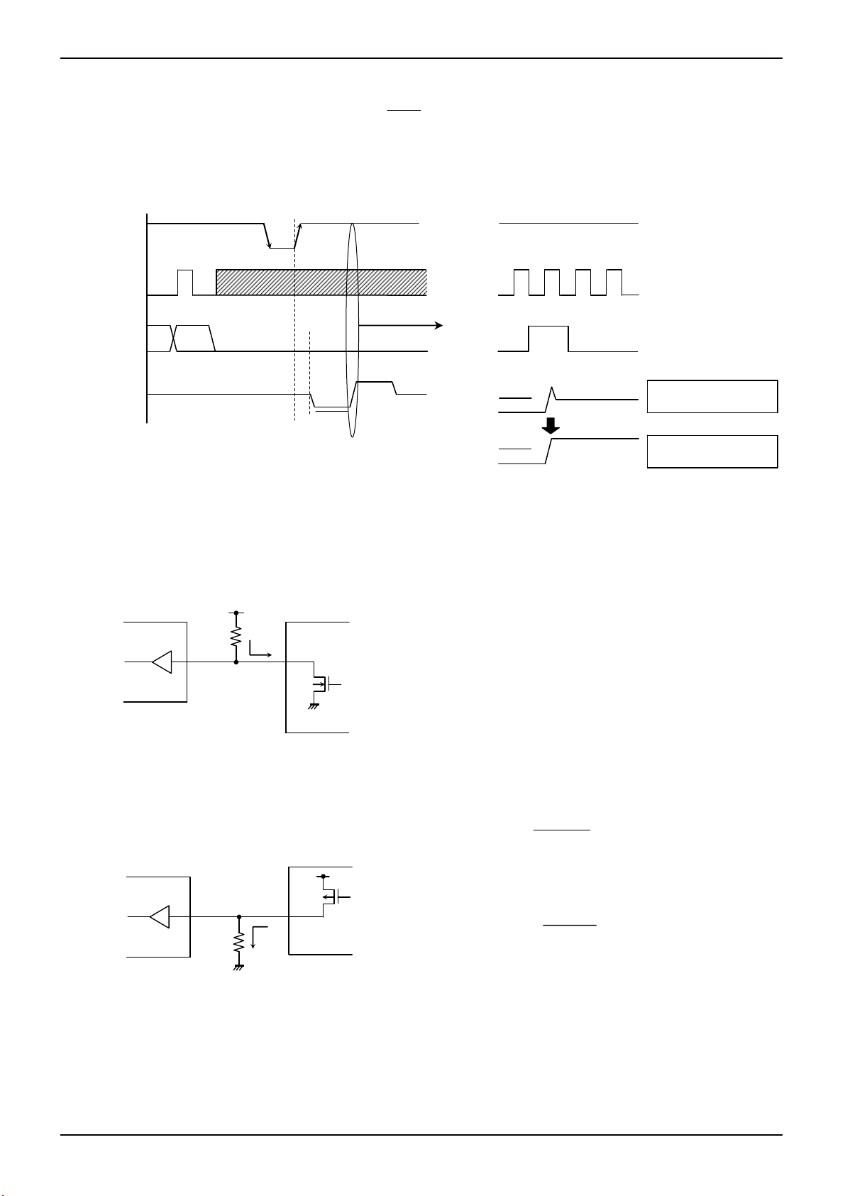
●Synchronous data input/output timing
CS
tCSS tSKH
tSKL
tCSH
SK
DO(READ)
tDIS tDIH
DI
tPD0
tPD1
tDF
DO(WRITE)
STAT U S VALID
Fig.1 Sync data input / output timing
○Data is taken by DI in sync with the rise of SK.
○At read action, data is output from DO in sync with the rise of SK.
○The status signal at write (READY /
BUSY ) is output after tCS from the fall of CS after write command input, at the area
DO where CS is “H”, and valid until the next command start bit is input. And, while CS is “L”, DO becomes High-Z.
○After completion of each mode execution, set CS “L” once for internal circuit reset, and execute the following action mode.
www.rohm.com
© 2011 ROHM Co., Ltd. All rights reserved.
2/16
2011.01 - Rev.
BU9888FV-W
A
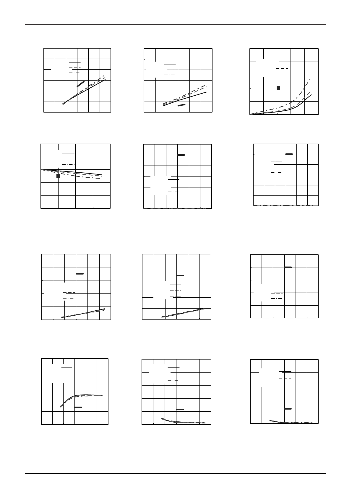
●Characteristic data (The following characteristic data are Typ. Values.)
6
5
(V)
Ta=-40℃
IH
Ta=25℃
4
Ta=85℃
3
SPEC
2
H INPUT VOLTAGE : V
1
0
0123456
SUPPLY VOLTAGE : Vcc(V)
Fig.2 'H' input
Fig.2 'H' input tvoltage
IH(CS,SK,DI)
5
(V)
4
OH
V
Ta=-40℃
Ta=25℃
voltage
V
(CS,SK,DI)
IH
Ta=85℃
3
SPEC
2
1
H OUTPUT VOLTAGE : V
0
0 0.4 0.8 1.2 1.6
H OUTPUT CURRENT : I
Fig.5 'H' output voltage
Fig.5 'H' output voltage VOH-IOH(Vcc=3.0V) Fig.6
OH-IOH(Vcc=3.0V)
V
(mA)
OH
6
5
(V)
IL
Ta=-40℃
4
Ta=25℃
=
3
2
L INPUT VOLTAGE : V
1
0
0123456
SUPPLY VOLTAGE : Vcc(V)
Fig.3 'L' input voltage V
Fig.3 'L' input voltage
IL (CS,SK,DI)
1.2
V
SPEC
(CS,SK,DI)
IL
SPEC
1
(uA )
LI
0.8
0.6
Ta=-40℃
Ta=25℃
0.4
Ta=85℃
0.2
INP UT L EAK C UR R E NT : I
0
0123456
SUPPLY VOLTAGE : Vcc(V)
Fig.6 Input leak current
Input leak current
LI(CS,SK,DI)
I
ILI(CS,SK,DI) Fig.7
1
(V)
0.8
Ta=-40℃
OL
Ta=25℃
Ta=85℃
0.6
0.4
0.2
L OUTPUT VOLTAGE : V
0
1.2
(uA)
LO
0.8
0.6
0.4
0.2
OUTPUT LEAK CURRENT : I
SPEC
012345
L OUTPUT CURRENT : I
Fig.4 'L' output voltage
Fig.4 'L' output voltage VOL-IOL(Vcc=3.0V)
OL-IOL(Vcc=3.0V)
V
1
Ta=-40℃
Ta=25℃
Ta=85℃
0
0123456
SUPPLY VOLTAGE : Vcc(V)
Fig.7 Output leak current
Output leak current
5
4
3
Ta=-40℃
Ta=25℃
2
Ta=85℃
AT W R ITING : Ic c1 (mA )
1
CURRENT CONSUMPTION
SPEC
0
0123456
Fig.8 Current consumption at WRITE
10000
1000
100
10
SUPPLY VOLTAGE : Vcc(V)
Fig.8
Current consumption at WRITE action
1(fSK=2MHz)
I
action ICC1(fSK=2MHz)
CC
Ta=-40℃
Ta=25℃
Ta=85℃
1
SK FRE Q U EN C Y : fSK ( MHz )
0.1
0123456
SUPPLY VOLTAGE : Vcc(V)
Fig.11 SK frequency fSK Fig.12 SK high time tSKH Fig.13 SK low time tSKL
Fig.11 SK frequency f
SPEC
SK
3
2.5
SPEC
2
1.5
AT READING : Icc2(mA)
0.5
CURRENT CONSUMPTION
Fig.9 Consumption current at READ
Ta=-40℃
Ta=25℃
Ta=85℃
1
0
0123456
SUPPLY VOLTAGE : Vcc(V)
Fig.9
Consumption current at READ
CC2(fSK=2MHz)
action I
1
action
I
2(fSK=2MHz)
CC
Ta=-40℃
0.8
(μ s)
SKH
H SK TIME : t
Ta=25℃
Ta=85℃
0.6
0.4
0.2
0
0123456
SUPPLY VOLTAGE : Vcc(V)
Fig.12 SK high time t
SPEC
SKH
2.5
(uA)
2
SB
1.5
Ta=-40℃
Ta=25℃
1
Ta=85℃
0.5
ST AND B Y CU R R EN T : I
0
0123456
SUPPLY VOLTAGE : Vcc(V)
Fig.10 Consumption current
Fig.10
Consumption current at standby action
at standby action I
1
Ta=-40℃
0.8
(μ s)
SKL
L SK TIME : t
Ta=25℃
Ta=85℃
0.6
0.4
0.2
0
0123456
SUPPLY VOLTAGE : Vcc(V)
Fig.13 SK
Technical Note
(mA)
OL
SPEC
SPEC
SPEC
low time
ILO(DO)
SB
t
SKL
LO(DO)
I
I
SB
www.rohm.com
© 2011 ROHM Co., Ltd. All rights reserved.
3/16
2011.01 - Rev.
BU9888FV-W
A
Technical Note
●Characteristic data (The following characteristic data are Typ. Values.)
1.2
1
0.8
(μ s)
Ta=-40℃
CS
Ta=25℃
0.6
Ta=85℃
0.4
L CS TIME : t
0.2
0
0123456
SUPPLY VOLTAGE : Vcc(V)
Fig.14 CS Low time tCS Fig.15 CS Setup time tCSS Fig.16 DI Hold time tDIH
Fig.14 CS
SPEC
loe time
300
200
(ns)
CSS
100
0
SPEC
Ta=-40℃
Ta=25℃
-100
CS S E T U P TIM E : t
t
CS
Ta=85℃
-200
0123456
SUPPLY VOLTAGE : Vcc(V)
Fig.15
CS setup time
t
CSS
150
SPEC
100
(ns)
DIH
Ta=-40℃
Ta=25℃
50
Ta=85℃
0
DI HO LD T IME : t
-50
0123456
SUPPLY VOLTAGE : Vcc(V)
Fig.16
DI hold time
150
(ns)
100
DIS
50
Ta=-40℃
Ta=25℃
Ta=85℃
SPEC
0
DI S ET U P TIM E : t
-50
0123456
SUPPLY VOLTAGE : Vcc(V)
Fig.17 DI Setup time tDIS Fig.18 Data '0' output delay time tPD0 Fig.19 Data '1' output delay time tPD1
Fig.17
DI setup time t
DIS
1
(μ s)
PD0
Ta=-40℃
0.8
Ta=25℃
Ta=85℃
0.6
0.4
SPEC
0.2
0
DA T A '0' OU T PUT D ELA Y TIM E : t
0123456
SUPPLY VOLTAGE : Vcc(V)
Fig.18
'0' output delay time t
Data
PD0
1
(μ s )
PD1
0.8
Ta=-40℃
Ta=25℃
0.6
Ta=85℃
0.4
0.2
0
DATA '1' OUTPUT DELAY TIME : t
0123456
SUPPLY VOLTAGE : Vcc(V)
SPEC
Fig.19 Data '1' output delay time t
1
Ta=-40℃
0.8
Ta=25℃
Ta=85℃
(μ s)
SV
0.6
0.4
TIME BETWEEN CS
0.2
AN D O U T PU T : t
0
0123456
SUPPLY VOLTAGE : Vcc(V)
Fig.20 Time from CS to output
Fig.20
Time from
establishment t
SPEC
CS to output establishment t
SV
SV
250
Ta=-40℃
(ns)
Ta=25℃
200
DF
Ta=85℃
150
SPEC
100
TIME BETWEEN CS
50
AND OUTPUT HIGH-Z : t
0
0123456
SUPPLY VOLTAGE : Vcc(V)
Fig.21 Time from CS to High-Z tDF Fig.22 Write cycle time tE/W
Fig.21 Time from CS to High-Z t
DF
5
Ta=-40℃
4
(ms)
Ta=25℃
E/W
Ta=85℃
3
SPEC
2
1
WRITE CYCLE TIME : t
0
0123456
SUPPLY VOLTAGE : Vcc(V)
Fig.22
Write cycle time
t
DIH
PD1
t
E/W
www.rohm.com
© 2011 ROHM Co., Ltd. All rights reserved.
4/16
2011.01 - Rev.
BU9888FV-W
A
High
Technical Note
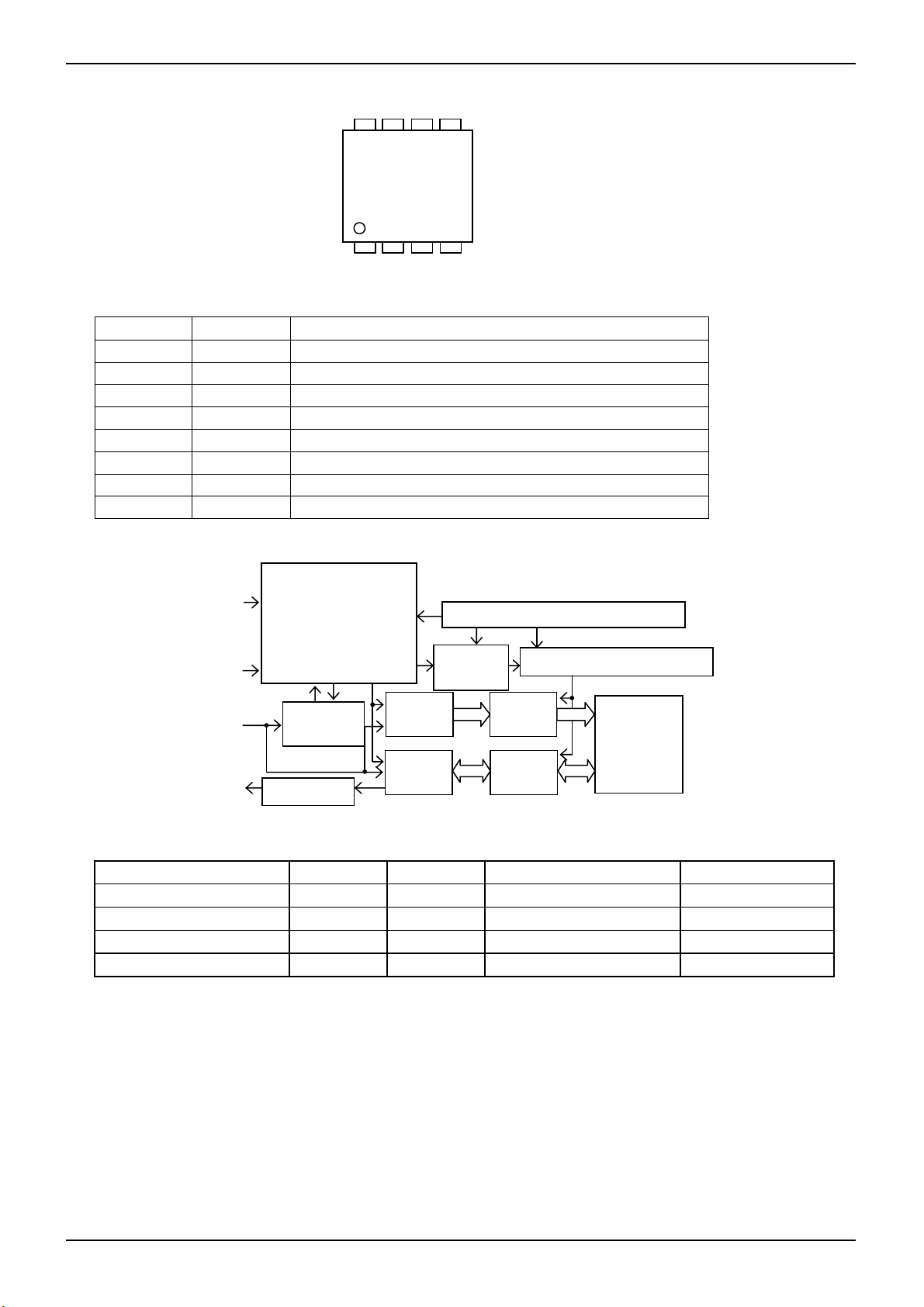
●Pin assignment
TEST1
TEST2
Vcc
GND
BU9888FV-W: SSOP-B8
CS SK DI
DO
Fig.23 Pin assignment diagram
●Pin function
Pin name I / O Function
CS Input Chip select input
SK Input Serial clock input
DI Input Serial data input
DO Output Serial data output
TEST1 Input Test pin. Please connect to power.
TEST2 - Test pin. Please open at using.
Vcc - Power source
GND - All input / output reference voltage, 0V
●Block diagram
CS
SK
Command decode
Control
Clock generation
Power source voltage detection
Write
prohibition
voltage occurrence
DI
Command
register
DO
Dummy bit
Address
buffer
Data
register
Fig.24 Block diagram
8bit
16bit
Address
decoder
R/W
amplifier
8bit
16bit
4,096bit
EEPROM
●Command mode
Command Start bit Ope code Address Data
Read (READ)
Write enable (WEN)
Write (WRITE)
Write disable (WDS)
(*1)
(*2)
1 10 A7, A6, A5, A4, A3, A2,A1, A0 D15~D0(READ DATA)
1 00 1 1 * * * * * *
1 01 A7, A6, A5, A4, A3, A2, A1, A0 D15~D0(WRITE DATA)
1 00 0 0 * * * * * *
・Input the address and the data in MSB first manners.
・As for *, input either VIH or VIL.
*Start bit
Acceptance of all the commands of this IC starts at recognition of the start bit.
The start bit means the first “1” input after the rise of CS.
*1 As for read, by continuous SK clock input after setting the read command, data output of the set address starts, and
address data in significant order are sequentially output continuously. (Auto increment function)
*2 When the read and the write all commands are executed, data written in the selected memory cell is automatically
deleted, and input data is written.
www.rohm.com
© 2011 ROHM Co., Ltd. All rights reserved.
5/16
2011.01 - Rev.
BU9888FV-W
A
Technical Note
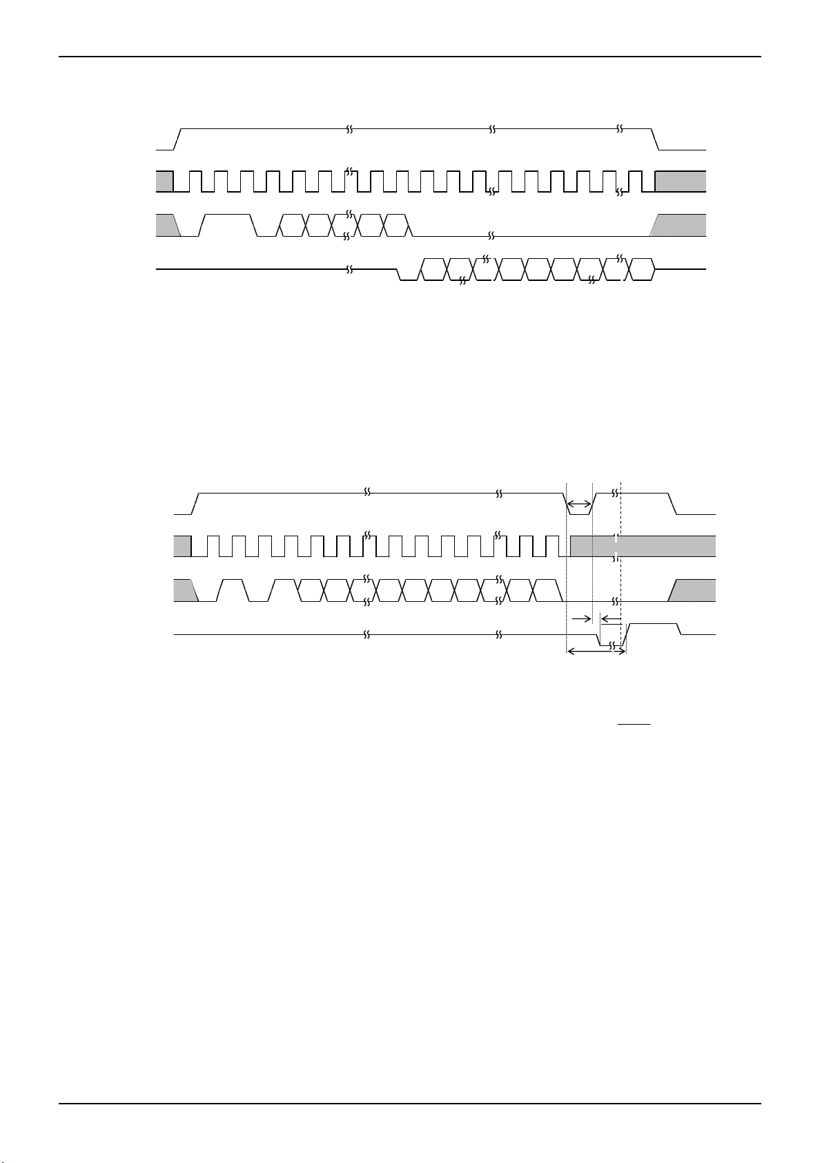
●Timing chart
1. Read cycle (READ)
CS
SK
DI
DO
High-Z
(※1)
12 4
1 1 A7 A6
~ ~
~ ~
~ ~
~ ~
~ ~
A0
A10
0
Fig.25 Read cycle
~ ~
~ ~
~ ~
~ ~
~ ~
28
(※2)
D027D1512D14D15 D14 D1
(※2)Next address data(Auto increment function)
~ ~
~ ~
~ ~
~ ~
(※1) Start bit
When data “1” is input for the first time after the rise of CS, this is recognized as a start bit. And when “1” is input after plural “0” are input, it is recognized
as a start bit, and the following operation is started. This is common to all the commands to described hereafter.
○When the read command is recognized, input address data (16bit) is output to serial. And at that moment, at taking A0,
in sync with the rise of SK, “0” (dummy bit) is output. And, the following data is output in sync with the rise of SK. This IC
has an address auto increment function valid only at read command. This is the function where after the above read
execution, by continuously inputting SK clock, the above address data is read sequentially. And, during the auto
increment, keep CS at “H”.
2. Write cycle (WRITE)
CS
SK
DI
DO
High-Z
12 4 11
~ ~
~ ~
~ ~
A1 A00
~ ~
~ ~
12 27
Fig.26 Write cycle
tE/W
tSV
~ ~
~ ~
STATUS
~ ~
~ ~
~ ~
READYBUSY
~ ~
~ ~
~ ~
~ ~
~ ~
tCS
D0D1D15 D141A7A61
○In this command, input 16bit data (D15~D0) are written to designated addresses (A7~A0). The actual write starts by the
fall of CS of D0 taken SK clock. When STATUS is not detected, (CS=”L” fixed) Max. 2ms in conformity with tE/W, and
when STATUS is detected (CS=”H”), all commands are not accepted for areas where “L” (
therefore, do not input any command.
BUSY ) is output from D0,
www.rohm.com
© 2011 ROHM Co., Ltd. All rights reserved.
6/16
2011.01 - Rev.

BU9888FV-W
A
3. Write enable (WEN)
○At power on, this IC is in write disable status by the internal RESET circuit. Before executing the write command, it is
necessary to execute the write enable command. And, once this command is executed, it is valid unitl the write disable
command is executed or the power is turned off. However, the read command is valid irrespective of write enable /
diable command. Input to SK after 8 clocks of this command is available by either “H” or “L”, but be sure to input it.
4. Write disable (WDS) cycle
CS
SK
DI
DO
12345
110 10
High-Z
Fig.27 Write enable (WEN) cycle
CS
SK
DI
12345
010
10 116789
10 116789
00
Technical Note
DO
High-Z
Fig.28 Write disable (WDS) cycle
○When the write enable command is executed after power on, write enable status gets in. When the write disable
command is executed then, the IC gets in write disable status as same as at power on, and then the write command is
canceled thereafter in software manner. However, the read command is executable. In write enable status, even when
the write command is input by mistake, write is started. To prevent such a mistake, it is recommended to execute the
write disable command after completion of write. Input to SK after 8 clocks of this command is available by either “H” or
“L”, but be sure to input it.
www.rohm.com
© 2011 ROHM Co., Ltd. All rights reserved.
7/16
2011.01 - Rev.

BU9888FV-W
A
b
●Application
1) Method to cancel each command
○READ
Start bit Ope code Address Data
1bit 2bit 8bit 16bit
Cancel is available in all areas in read mode.
・Method to cancel:cancel by CS=“L”
○WRITE
Start bit Ope code Address Data
1bit 2bit 8bit 16bit
a:From start bit to 27 clock rise
Cancel by CS=“L”
b:27 clock rise and after
Cancellation is not available by any means. If Vcc is made OFF in this area,
designated address data is not guaranteed, therefore write once again.
And when SK clock is input continuously, cancellation is not available.
2) At standby
○Standby current
When CS is “L”, SK input is “L”, DI input is “H”, and even with middle electric potential, current does not increase.
○Timing
As shown in Fig.31, when SK at standby is “H”, if CS is started, DI status may be read at the rise edge.
At standby and at power ON/OFF, when to start CS, set SK input or DI input to “L” status. (Refer to Fig.32)
CS=SK=DI=”H”
Wrong recognition as a start bit
CS
SK
DI
Fig.31 Wrong action timing
Fig.29 READ cancel available timing
・27 Rise of clock
SK
DI
a
Fig.30 Write cancel available timing
Start bit input
26
27
D1
D0
Enlarged figure
CS
SK
DI
Technical Note
tE/W
CS=SK=DI=”H”
Wrong recognition as a start bit
Start bit input
Fig.32 Normal action timing
www.rohm.com
© 2011 ROHM Co., Ltd. All rights reserved.
8/16
2011.01 - Rev.

BU9888FV-W
A
3) Equivalent circuit
Output circuit
Input circuit
SK
DI
4) I/O peripheral circuit
4-1) Pull down CS.
By making CS=“L” at power ON/OFF, mistake in operation and mistake write are prevented.
○Pull down resistance Rpd of CS pin
To prevent mistake in operation and mistake write at power ON/OFF, CS pull down resistance is necessary.
Select an appropriate value to this resistance value from microcontroller VOH, IOH, and VIL characteristics of this IC.
Microcontroller
“H” output
OEint.
Fig.33 Output circuit (DO)
CS int.
Fig.35 Input circuit (SK,DI)
EEPROM
VOHM
IOHM Rpd
VIHE
“L” input
Fig.37 CS pull down resistance
DO
Technical Note
Input circuit
RESET int.
CS
Fig.34 Input circuit (CS)
Input circuit
TEST1
VDD
Fig.36 Input circuit (TEST1)
VOHM
≧ ・・・①
Rpd
IOHM
≧ VIHE ・・・②
VOHM
Example) When V
from the equation ①,
∴ Rpd ≧ 1.2 [kΩ]
With the value of Rpd to satisfy the above equation, VOHM becomes
2.4V or higher, and VIHE (=2.0V), the equation ② is also satisfied.
・VIHE
・VOHM
・IOHM
=5V, VIHE=2V, VOHM=2.4V, IOHM=2mA,
CC
≧
Rpd
: EEPROM VIH specifications
: Microcontroller VOH specifications
: Microcontroller IOH specifications
2.4
2×10
-3
CSint.
www.rohm.com
© 2011 ROHM Co., Ltd. All rights reserved.
9/16
2011.01 - Rev.
BU9888FV-W
A
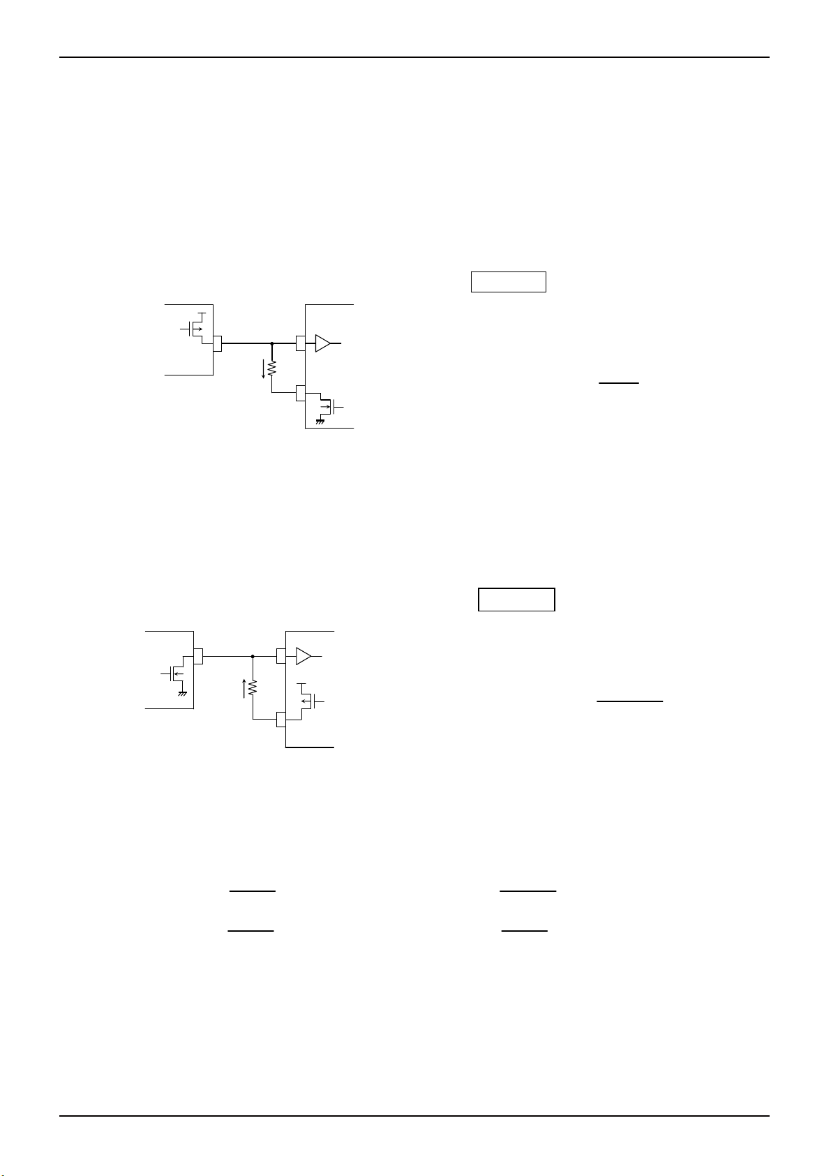
4-2) DO is available in both pull up and pull down.
Do output become “High-Z” in other READY /
command. When malfunction occurs at “High-Z” input of the microcontroller port connected to DO, it is necessary to
pull down and pull up DO. When there is no influence upon the microcontroller actions, DO may be OPEN.
If DO is OPEN, and at timing to output status READY, at timing of CS=“H”, SK=“H”, DI=“H”, EEPROM recognizes this
as a start bit, resets READY output, and DO=”High-Z”, therefore, READY signal cannot be detected. To avoid such
output, pull up DO pin for improvement.
CS
SK
DI
DO
D0
High-Z
○Pull up resistance Rpu and pull down resistance Rpd of DO pin
As for pull up and pull down resistance value, select an appropriate value to this resistance value from microcontroller
VIH, VIL, and VOH, IOH, VOL, IOL characteristics of this IC.
Microcontroller
VILM
“L” input
Rpu
IOLE
VOLE
Fig.39 DO pull up resistance
Microcontroller
VIHM
VOHE
“H” input
Rpd
IOHE
“H” output
Fig.40 DO pull down resistance
BUSY output timing than after data output at read command and write
CS
“H”
SK
Enlarged
READY
BUSY
DI
DO
DO
BUSY
BUSY
Fig.38 READY output timing at DO=OPEN
Rpu ≧ ・・・③
EEPROM
“L” output
EEPROM
Example) When V
from the equation ③,
∴ Rpu
With the value of Rpu to satisfy the above equation, VOLE becomes 0.4V
or below, and with VILM(=0.8V), the equation ④ is also satisfied.
・VOLE
・IOLE
・VILM
Example) When V
∴ Rpd
With the value of Rpd to satisfy the above equation, VOHE becomes 2.4V
or below, and with VIHM (=3.5V), the equation ⑥ is also satisfied.
・VOHE
・IOHE
・VIHM
≦ VILM ・・・④
VOLE
=5V, VOLE=0.4V, IOLE=2.1mA, VILM=0.8V,
CC
≧
Rpu
≧ 2.2 [kΩ]
: EEPROM VOL specifications
: EEPROM IOL specifications
: Microcontroller VIL specifications
≧ ・・・⑤
Rpd
VOHE
≧ VIHM ・・・⑥
=5V, VOHE=Vcc-0.2V, IOHE=0.1mA,
CC
VIHM=Vcc×0.7V from the equation ⑤,
Rpd
≧
≧ 48 [kΩ]
: EEPROM VOH specifications
: EEPROM IOH specifications
: Microcontroller VIH specifications
High-Z
Improvement by DO pull up
READY
VOHE
IOHE
5-0.2
-3
0.1×10
Technical Note
CS=SK=DI=”H”
When DO=OPEN
CS=SK=DI=”H”
When DO=pull up
www.rohm.com
© 2011 ROHM Co., Ltd. All rights reserved.
10/16
2011.01 - Rev.

BU9888FV-W
A
Technical Note
5) READY /
BUSY status display (DO terminal)
(common to BR93L46-W / A46-WM,BR93L56-W / A56-WM, BR93L66-W / A66-WM, BR93L76-W / A76-WM, BR93L86-W /
A86-WM)
This display outputs the internal status signal. When CS is started after tCS (Min.200ns)
from CS fall after write command input, “H” or “L” is output.
B/R display=“L” ( BUSY ) = write under execution
(DO status)
After the timer circuit in the IC works and creates the period of tE/W, this time circuit completes automatically.
And write to the memory cell is made in the period of tE/W, and during this period, other command is not accepted.
B/R
display = “H” (READY) = command wait status
(DO status)
Even after tE/W (max.5ms) from write of the memory cell, the following command is accepted.
Therefore, CS=“H” in the period of tE/W, and when input is in SK, DI, malfunction may occur, therefore, DI=“L” in the
area
CS=“H”. (Especially, in the case of shared input port, attention is required.)
* Do not input any command while status signal is output.
Command input in
BUSY area is cancelled, but command input in READY area is accepted.
Therefore, status READY output is cancelled, and malfunction and mistake write may be made.
CS
STATUS
SK
CLOCK
DI
DO
High-Z
WRITE
INSTRUCTION
tSV
READY
BUSY
Fig.41 B/R status output timing chart
www.rohm.com
© 2011 ROHM Co., Ltd. All rights reserved.
11/16
2011.01 - Rev.
BU9888FV-W
A
Technical Note
6) When to directly connect DI and DO
This IC has independent input terminal DI and output terminal DO, and separate signals are handled on timing chart,
meanwhile, by inserting a resistance R between these DI and DO terminals, it is possible to carry out control by 1 control
line.
Microcontroller
DI/O PORT
R
EEPROM
DI
DO
Fig.42 DI, DO control line common connection
○Data collision of microcontroller DI/O output and DO output and feedback of DO output to DI input.
Drive from the microcontroller DI/O output to DI input on I/O timing, and signal output from DO output occur at the same
time in the following points.
(1) 1 clock cycle to take in A0 address data at read command
Dummy bit “0” is output to DO terminal.
→When address data A0 = “1” input, through current route occurs.
Fig.43 Collision timing at read data output at DI, DO direct connection
(2) Timing of CS = “H” after write command. DO terminal in READY /
EEPROM CS input
EEPROM SK input
EEPROM DI input
EEPROM DO output
Microcontroller DI/O port
Microcontroller output Microcontroller in put
“H”
High-Z
A1
A0
A1 A0
Collision of DI input and DO output
D15 D14 D13
0
High-Z
BUSY function output.
When the next start bit input is recognized, “HIGH-Z” gets in.
→Especially, at command input after write, when CS input is started with microcontroller DI/O output “L”,
READY output “H” is output from DO terminal, and through current route occurs.
Feedback input at timing of these (1) and (2) does not cause disorder in basic operations, if resistance R is inserted.
EEPROM CS input
EEPROM SK input
EEPROM DI input
EEPROM DO output
Microcontroller DI/O port
Write command
Write command
Write command
Write command
Write command
Microcontrol ler output
~ ~
~ ~
~ ~
BUSY
~ ~
BUSY
~ ~
Microcontroller input Microcontroller output
READY
READY
~ ~
~ ~
~ ~
~ ~
READY
~ ~
High-Z
Collision of DI input and DO output
Fig.44 Collision timing at DI, DO direct connection
Note) As for the case (2), attention must be paid to the following.
When status READY is output, DO and DI are shared, DI=”H” and the microcontroller DI/O=”High-Z” or the
microcontroller DI/O=”H”,if SK clock is input, DO output is input to DI and is recognized as a start bit, and malfunction
may occur. As a method to avoid malfunction, at status READY output, set SK=“L”, or start CS within 4 clocks after “H”
of READY signal is output.
CS
SK
DI
DO
READY
Fig.45 Start bit input timing at DI, DO direct connection
Start bit
High-Z
Because DI=”H”, set
SK=”L” at CS rise.
www.rohm.com
© 2011 ROHM Co., Ltd. All rights reserved.
12/16
2011.01 - Rev.
BU9888FV-W
A
Cond
s
Technical Note
○Selection of resistance value R
The resistance R becomes through current limit resistance at data collision. When through current flows, noises of power
source line and instantaneous stop of power source may occur. When allowable through current is defined as I, the
following relation should be satisfied. Determine allowable current amount in consideration of impedance and so forth of
power source line in set. And insert resistance R, and set the value R to satisfy EEPROM input level VIH/VIL even under
influence of voltage decline owing to leak current and so forth. Insertion of R will not cause any influence upon basic
operations.
(1) Address data A0 = “1” input, dummy bit “0” output timing
(When microcontroller DI/O output is “H”, EEPROM DO outputs “L”, and “H” is input to DI)
・Make the through current to EEPROM 10mA or below.
・See to it that the level VIH of EEPROM should satisfy the following.
Microcontroller
“H” output
DI/O PORT
VOHM
IOHM
EEPROM
DI
R
DO
VOLE
“L” output
ition
VOHM ≦ VIHE
VOHM ≦ IOHM×R + VOLE
At this moment, if VOLE=0V,
VOHM ≦ IOHM×R
∴ R ≧ ・・・⑦
・VIHE
・VOLE
・VOHM
・IOHM
: EEPROM VIH specifications
: EEPROM VOL specifications
: Microcontroller VOH specifications
: Microcontroller IOH specifications
VOHM
IOHM
Fig.46 Circuit at DI, DO direct connection (Microcontroller DI/O “H” output, EEPROM “L” output)
(2) DO status READY output timing
(When the microcontroller DI/O is “L”, EEPROM DO output “H”, and “L” is input to DI)
・Set the EEPROM input level VIL so as to satisfy the following.
Microcontroller
“L” output
DI/O PORT
VOLM
EEPROM
DI
IOHM
R
VOHE
DO
“H” output
Fig.47 Circuit at DI, DO direct connection (Microcontroller DI/O “L” output, EEPROM “H” output)
Conditions
VOLM ≧ VILE
VOLM ≧ VOHE – IOLM×R
As this moment, VOHE=Vcc
VOLM ≧ Vcc – IOLM×R
∴ ・・・⑧
・VILE
・VOHE
・VOLM
・IOLM
: EEPROM VIL specifications
: EEPROM VOH specifications
: Microcontroller VOL specifications
: Microcontroller IOL specifications
Vcc – VOLM
IOLM
Example) When Vcc=5V, VOHM=5V, IOHM=0.4mA, VOLM=5V, IOLM=0.4mA,
From the equation ⑦, From the equation⑧,
R ≧
R ≧
∴ R ≧ 12.5 [kΩ] ・・・⑨
VOHM
IOHM
5
0.4×10
-3
∴ R ≧ 2.2 [kΩ] ・・・⑩
Therefore, from the equations ⑨ and ⑩,
∴ R ≧ 12.5 [kΩ]
R ≧
R ≧
Vcc – VOLM
IOLM
5 – 0.4
-3
2.1×10
www.rohm.com
© 2011 ROHM Co., Ltd. All rights reserved.
13/16
2011.01 - Rev.

BU9888FV-W
A
p
7) Notes on power ON/OFF
・At power ON/OFF, set CS “L”.
When CS is “H”, this IC gets in input accept status (active). If power is turned on in this status, noises and the likes may
cause malfunction, mistake write or so. To prevent these, at power ON, set CS “L”. (When CS is in “L” status, all inputs
are cancelled.) And at power decline, owing to power line capacity and so forth, low power status may continue long. At
this case too, owing to the same reason, malfunction, mistake write may occur, therefore, at power OFF too, set CS “L”.
(Bad example)CS pin is pulled up to Vcc.
In this case, CS becomes “H” (active status), and EEPROM may have malfunction,
mistake write owing to noise and the likes.
Even when CS in
○POR citcuit
This IC has a POR (Power On Reset) circuit as a mistake write countermeasure. After POR action, it gets in write
disable status. The POR circuit is valid only when power is ON, and does not work when power is OFF. However, if CS
is “H” at power ON/OFF, it may become write enable status owing to noises and the likes. For secure actions, observe
the follwing conditions.
1. Set CS=”L”
2. Turn on power so as to satisfy the recommended conditions of tR, tOFF, Vbot for POR circuit action.
VCC
0
○LVCC circuit
LVCC (VCC-Lockout) circuit prevents data rewrite action at low power, and prevents wrong write.
At LVCC voltage (Typ.=1.2V) or below, it prevent data rewrite.
8) Noise countermeasur es
○VCC noise (bypass capacitor)
When noise or surge gets in the power source line, malfunction may occur, therefore, for removing these, it is
recommended to attach a bypass capacitor (0.1μF) between IC VCC and GND, At that moment, attach it as close to IC
as possible.And, it is also recommended to attach a bypass capacitor between board VCC and GND.
○SK noise
When the rise time (tR) of SK is long, and a certain degree or more of noise exists, malfunction may occur owing to clock
bit displacement. To avoid this, a Schmitt trigger circuit is built in SK input. The hysteresis width of this circuit is set about
0.2V, if noises exist at SK input, set the noise amplitude 0.2Vp-p or below. And it is recommended to set the rise time
(tR) of SK 100ns or below. In the case when the rise time is 100ns or higher, take sufficient noise countermeasures.
Make the clock rise, fall time as small as possible.
VCC
VCC
GND
VCC
CS
GND
Bad example Good example
Fig.48 Timing at power ON/OFF
ut is High-Z, the status becomes like this case, which please note.
t
R
t
OFF
Vbot
10ms or below 10ms or higher 0.3V or below
100ms or below 10ms or higher 0.2V or below
Fig.49 Rise waveform diagram
Technical Note
(Good example)It is “L” at power ON/OFF.
Set 10ms or higher to recharge at power OFF.
When power is turned on without observing this condition,
IC internal circuit may not be reset, which please note.
Recommended conditions of tR, tOFF, Vbot
t
t
R
Vbot
OFF
www.rohm.com
© 2011 ROHM Co., Ltd. All rights reserved.
14/16
2011.01 - Rev.

BU9888FV-W
A
●Notes for use
(1) Described numeric values and data are design representative values, and the values are not guaranteed.
(2) We believe that application circuit examples are recommendable, however, in actual use, confirm characteristics further
sufficiently. In the case of use by changing the fixed number of external parts, make your decision with sufficient margin in
consideration of static characteristics and transition characteristics and fluctuations of external parts and our LSI.
(3) Absolute Maximum Ratings
If the absolute maximum ratings such as impressed voltage and action temperature range and so forth are exceeded, LSI
may be destructed. Do not impress voltage and temperature exceeding the absolute maximum ratings. In the case of fear
exceeding the absolute maximum ratings, take physical safety countermeasures such as fuses, and see to it that
conditions exceeding the absolute maximum ratings should not be impressed to LSI.
(4) GND electric potential
Set the voltage of GND terminal lowest at any action condition. Make sure that each terminal voltage is not lower than that
of GND terminal in consideration of transition status.
(5) Heat design
In consideration of allowable loss in actual use condition, carry out heat design with sufficient margin.
(6) Terminal to terminal short-circuit and wrong packaging
When to package LSI onto a board, pay sufficient attention to LSI direction and displacement. Wrong packaging may
destruct LSI. And in the case of short-circuit between LSI terminals and terminals and power source, terminal and GND
owing to foreign matter, LSI may be destructed.
(7) Use in a strong electromagnetic field may cause malfunction, therefore, evaluate design sufficient.
Technical Note
www.rohm.com
© 2011 ROHM Co., Ltd. All rights reserved.
15/16
2011.01 - Rev.

BU9888FV-W
A
●Ordering part number
B U 9 8 8 8 F V - W E 2
Part No. Part No.
SSOP-B8
3.0± 0.2
(MAX 3.35 include BURR)
5678
6.4± 0.3
4.4± 0.2
1.15± 0.1
0.1
(0.52)
1234
0.65
0.22
0.1
+0.06
−0.04
S
0.08
S
M
0.3MIN
0.15± 0.1
(Unit : mm)
Package
FV: SSOP-B8
<Tape and Reel information>
Embossed carrier tapeTape
Quantity
Direction
of feed
2500pcs
E2
The direction is the 1pin of product is at the upper left when you hold
()
reel on the left hand and you pull out the tape on the right hand
Reel
Packaging and forming specification
E2: Embossed tape and reel
1pin
Order quantity needs to be multiple of the minimum quantity.
∗
Direction of feed
Technical Note
www.rohm.com
© 2011 ROHM Co., Ltd. All rights reserved.
16/16
2011.01 - Rev.

Notes
No copying or reproduction of this document, in part or in whole, is permitted without the
consent of ROHM Co.,Ltd.
The content specied herein is subject to change for improvement without notice.
The content specied herein is for the purpose of introducing ROHM's products (hereinafter
"Products"). If you wish to use any such Product, please be sure to refer to the specications,
which can be obtained from ROHM upon request.
Examples of application circuits, circuit constants and any other information contained herein
illustrate the standard usage and operations of the Products. The peripheral conditions must
be taken into account when designing circuits for mass production.
Great care was taken in ensuring the accuracy of the information specied in this document.
However, should you incur any damage arising from any inaccuracy or misprint of such
information, ROHM shall bear no responsibility for such damage.
The technical information specied herein is intended only to show the typical functions of and
examples of application circuits for the Products. ROHM does not grant you, explicitly or
implicitly, any license to use or exercise intellectual property or other rights held by ROHM and
other parties. ROHM shall bear no responsibility whatsoever for any dispute arising from the
use of such technical information.
The Products specied in this document are intended to be used with general-use electronic
equipment or devices (such as audio visual equipment, ofce-automation equipment, communication devices, electronic appliances and amusement devices).
The Products specied in this document are not designed to be radiation tolerant.
While ROHM always makes efforts to enhance the quality and reliability of its Products, a
Product may fail or malfunction for a variety of reasons.
Please be sure to implement in your equipment using the Products safety measures to guard
against the possibility of physical injury, re or any other damage caused in the event of the
failure of any Product, such as derating, redundancy, re control and fail-safe designs. ROHM
shall bear no responsibility whatsoever for your use of any Product outside of the prescribed
scope or not in accordance with the instruction manual.
The Products are not designed or manufactured to be used with any equipment, device or
system which requires an extremely high level of reliability the failure or malfunction of which
may result in a direct threat to human life or create a risk of human injur y (such as a medical
instrument, transportation equipment, aerospace machinery, nuclear-reactor controller, fuelcontroller or other safety device). ROHM shall bear no responsibility in any way for use of any
of the Products for the above special purposes. If a Product is intended to be used for any
such special purpose, please contact a ROHM sales representative before purchasing.
If you intend to export or ship overseas any Product or technology specied herein that may
be controlled under the Foreign Exchange and the Foreign Trade Law, you will be required to
obtain a license or permit under the Law.
Notice
www.rohm.com
© 2011 ROHM Co., Ltd. All rights reserved.
Thank you for your accessing to ROHM product informations.
More detail product informations and catalogs are available, please contact us.
ROHM Customer Support System
http://www.rohm.com/contact/
R1120
A
 Loading...