


Memory for Plug & Play
I2C BUS3Ports for HDMI Port
Serial EEPROM
BU9883FV-W
● Description
BU9883FV-W is for DDC 3 ports, 2K x 8 bit array 3 BANK EEPROM.
●Features
1) There are 3 BANKs, 1 BANK compose of 256 word address x 8 bit EEPROM
2) There are 3 DDC interface channels, and each channel can access each BANK independently from other ports.
3) 2K bit X 3 BANK memory bits can be accessed from write port (Port0).
4) Operate voltage (3.0V~5.5V)
5) Built in diode for power supply from HDMI ports and system.
6) Automatic erase
7) 8 byte page write mode
8) Low power consumption
Active ( 5.0V ) : 1.2mA (Typ.)
Standby ( 5.0V ) : 100μA(Max.)
9) DATA security
10) Write Protect pin can switch write port
11) Inhibit to WRITE at low VCC
12) Pin package : SSOP16pin
13) Endurance : 1,000,000 erase/write cycles
14) Data retention 40 years
15) Filtered inputs in all SCL・SDA for noise suppression
16) Shipment data all address FFh
●Absolute maximum rating (Ta=25℃)
Parameter Symbol Rating Unit
Supply Voltage VCC -0.3~6.5 V
Power Dissipation Pd 400 *1 mW
Storage Temperature Tstg -65 ~ 125 ℃
Operating Temperature Topr -40 ~ 85 ℃
Terminal Voltage - -0.3~VCC+0.3 *1 V
*1 Degradation is done at 3.0mW/℃ for operation above 25℃
*2 The Max value of terminal voltage is not over 6.5V
●EEPROM recommended operating condition
Parameter Symbol Rating Unit
Supply Voltage VCC 3.0~5.5
Input Voltage VIN 0 ~ VCC0~3
No.09002EBT01
V
www.rohm.com
© 2009 ROHM Co., Ltd. All rights reserved.
1/18
2009.04 - Rev.B

BU9883FV-W
Technical Note
●Memory cell characteristics(Ta=25℃, VCC0~3 = 3.0~5.5V)
Parameter
Min. Typ. Max.
Specification
Unit
Write/Erase Cycle *1 1,000,000 - - Cycles
Data Retention *1 40 - - Years
*1:Not 100% TESTED
●Input/output capacity (Ta=25℃, Frequency=5MHz)
Parameter Symbol Min. Typ. Max. Unit
SDA pins (SDA0,1,2,3)
*1
Cin - 7 - pF
SCL pins (SCL0,1,2,3) *1 Cin2 - 7 - pF
*1:Not 100% TESTED
●EEPROM DC operating characteristics (Unless otherwise specified, Ta=-40~85℃, VCC0~3 = 3.0~5.5V)
Parameter Symbol
Specification
Min. Typ. Max.
Unit Test condition
"H" Input Voltage0 VIH0 0.7xVCC0 - VCC0+0.5 V 3.0≦VCC0≦5.5V(SCL0, SDA0)
"L" Input Voltage0 VIL0 -0.3 - 0.3xVCC0 V 3.0≦VCC0≦5.5V(SCL0, SDA0)
"H" Input Voltage1 VIH1 0.7xVCC1 - VCC1+0.5 V 3.0≦VCC1≦5.5V(SCL1, SDA1)
"L" Input Voltage1 VIL1 -0.3 - 0.3xVCC1 V 3.0≦VCC1≦5.5V(SCL1, SDA1)
"H" Input Voltage2 VIH2 0.7xVCC2 - VCC2+0.5 V 3.0≦VCC2≦5.5V(SCL2, SDA2)
"L" Input Voltage2 VIL2 -0.3 - 0.3xVCC2 V 3.0≦VCC2≦5.5V(SCL2, SDA2)
"H" Input Voltage3 VIH3 0.7xVCC3 - VCC3+0.5 V 3.0≦VCC3≦5.5V(SCL3, SDA3)
"H" Input Voltage3 VIL3 -0.3 - 0.3xVCC3 V 3.0≦VCC3≦5.5V(SCL3, SDA3)
"L" Output Voltage0 VOL0 - - 0.4 V IOL=3.0mA , 3.0V≦VCC0≦5.5V(SDA0)
"L" Output Voltage1 VOL1 - - 0.4 V IOL=3.0mA , 3.0V≦VCC1≦5.5V(SDA1)
"L" Output Voltage2 VOL2 - - 0.4 V IOL=3.0mA , 3.0V≦VCC2≦5.5V(SDA2)
"L" Output Voltage3 VOL3 - - 0.4 V IOL=3.0mA , 3.0V≦VCC3≦5.5V(SDA3)
WP "H" Input Voltage VIH4 0.7xVCC0 - VCC0+0.3 V 3.0≦VCC0≦5.5V(WPB)
WP "L" Input Voltage VIL4 -0.3 - 0.3xVCC V 3.0≦VCC0≦5.5V(WPB)
Input Leakage Current0 ILI0 -1 - 1 μA VIN=0~5.5V(SCL0~3)
Input Leakage Current1 ILI1 55 110 230 μA WPB=5.5V , VCC=5.5V
Output Leakage Current0 ILO0 -1 - 1 μA VOUT=0~5.5(SDA0~3)
ICC1 - - 2.0 mA
Operating Current
ICC2 - - 1.0 mA
VCC0=5.5V, fSCL=400kHz,tWR=5ms
Byte Write, Page Write
VCC0~3=5.5V, fSCL=400kHz
Random Read, Current Read,Sequential
Read, (each port operation)
Standby Current ISB0 - - 100 μA
Standby Current ISB1 - - 100 μA
Standby Current ISB2 - - 100 μA
Standby Current ISB3 - - 100 μA
○This product is not designed for protection against radioactive rays.
VCC~0=5.5V, SDA0~3=SCL0~3=5.5V,
WPB=GND
VCC1=5.5V, SDA0~3=SCL0~3=5.5V,
WPB=GND
VCC2=5.5V, SDA0~3=SCL0~3=5.5V,
WPB=GND
VCC3=5.5V, SDA0~3=SCL0~3=5.5V,
WPB=GND
www.rohm.com
© 2009 ROHM Co., Ltd. All rights reserved.
2/18
2009.04 - Rev.B
BU9883FV-W
Technical Note
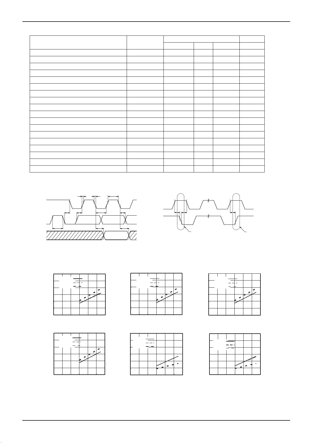
●EEPROM AC operating characteristics (Ta=-40~85℃, VCC0~3 = 3.0~5.5V)
Parameter Symbol
3.0≦VCC0~3≦5.5V Unit
Min. Typ. Max. Min.
Clock Frequency fSCL - - 400 kHz
Data Clock High Period tHIGH 0.6 - - μs
Data Clock Low Period tLOW 1.2 - - μs
SDA0~3 and SCL0~3 Rise Time *1 tR - - 0.3 μs
SDA0~3 and SCL0~3 Fall Time*1 tF - - 0.3 μs
Start Condition Hold Time tHD:STA 0.6 - - μs
Start Condition Setup Time tSU:STA 0.6 - - μs
Input Data Hold Time tHD:DAT 0 - - ns
Input Data Setup Time tSU:DAT 100 - - ns
Output Data Delay Time tPD 0.1 - 0.9 μs
Output Data Hold Time tDH 0.1 - - μs
Stop Condition Setup Time tSU:STO 0.6 - - μs
Bus Free Time tBUF 1.2 - - μs
Write Cycle Time tWR - - 5 ms
Noise Spike Width (SDA0~3 and SCL0~3) tI - - 0.1 μs
WP Hold Time tHD:WP 0 - - ns
WP Setup Time tSU:WP 0.1 - - μs
WP valid time tHIGH:WP 1.0 - - μs
*1 : Not 100% TESETED
●Synchronous data input/output timing
SCL
SDA
(IN)
SDA
(OUT)
tHD:STA tHD:DAT tSU:DAT
tBUF tPD tDH
tHIGH tR tF
tLOW
Fig.-1 SYNCHRONOUS DATA TIMING
SCL
tSU:STA tSU:STO tHD:STA
SDA
START BIT STOP BIT
○SDA data is latched into the chip at the rising edge of the SCL clock. (This is commoness in all port.)
○Output date toggles at the falling edge of the SCL clock. (This is commoness in all port.)
●Characteristic data (The following values are Typ. ones).
6
Ta=-40℃
5
[V]
Ta=25℃
IH0
Ta=85℃
4
3
2
1
H INPUT VOLTAGE0 : V
0
0123456
6
5
[V]
IH3
4
3
2
1
H INPUT VOLTAGE3 : V
0
0123456
SPEC
SUPPLY VOLTAGE
Fig.2 'H' Input Voltage0 V
(SCL0,SDA0)
Ta=-40℃
Ta=25℃
Ta=85℃
SUPPLY VOLTAGE : Vcc3[V]
Fig.5 'H' Input Voltage3 V
: Vcc0[V]
SPEC
(SCL3,SDA3)
IH0
IH3
6
Ta=-40℃
5
[V]
Ta=25℃
IH1
Ta=85℃
4
3
2
1
H INPUT VOLTAGE1 : V
0
0123456
6
5
[V]
IL0
4
3
2
1
L INPUT VOLTAGE0 : V
0
0123456
SPEC
SUPPLY VOLTAGE
Fig.3 'H' Input Voltage1 V
(SCL1,SDA1)
Ta=-40℃
Ta=25℃
Ta=85℃
SUPPLY VOLTAGE
Fig.6 'L' Input Voltage0 V
(SCL0,SDA0)
: Vcc0[V]
IH1
SPEC
: Vcc0[V]
IL0
6
Ta=-40℃
5
[V]
Ta=25℃
IH2
Ta=85℃
4
3
2
1
H INPUT VOLTAGE2 : V
0
0123456
6
5
[V]
IL1
4
3
2
1
L INPUT VOLTAGE1 : V
0
0123456
SPEC
SUPPLY VOLTAGE
Fig.4 'H' Input Voltage2 V
(SCL2,SDA2)
Ta=-40℃
Ta=25℃
Ta=85℃
SUPPLY VOLTAGE
Fig.7 'L' Input Voltage1 V
: Vcc2[V]
: Vcc1[V]
(SCL1,SDA1)
IH2
SPEC
IL 1
www.rohm.com
© 2009 ROHM Co., Ltd. All rights reserved.
3/18
2009.04 - Rev.B

BU9883FV-W
●Characteristic data (The following values are Typ. ones).
6
Ta=-40℃
5
[V]
Ta=25℃
IL2
Ta=85℃
4
3
2
1
L INPUT VOLTAGE2 : V
0
0123456
SUPPLY VOLTAGE
Fig.8 'L' Input Voltage2 V
(SCL2,SDA2)
1
[V]
Ta=-40℃
0.8
OL1
Ta=25℃
Ta=85℃
0.6
0.4
: Vcc2[V]
SPEC
0.2
L OUTPUT VOLTAGE1 : V
0
0123456
5
]
[V
4
IH4
3
2
1
WP H INPUT VOLTAGE : V
0
L OUTPUT CURRENT
Fig.11 'L' Output Voltage1
V
(Vcc1=
OL1-IOL
Ta=-40℃
Ta=25℃
Ta=85℃
012345678
L OUTPUT CURRENT
Fig.14
WP
: IOL[mA]
3.0V
)(SDA1)
SPEC
: Vcc0[V]
'H' Input Voltage V
SPEC
IL 2
IH4
6
]
Ta=-40℃
5
[V
Ta=25℃
IL3
Ta=85℃
4
3
2
1
L INPUT VOLTAGE3 : V
0
0123456
SUPPLY VOLTAGE : Vcc3[V]
Fig.9 'L' Input Voltage3 V
(SCL3,SDA3)
1
Ta=-40℃
[V]
Ta=25℃
0.8
OL2
Ta=85℃
0.6
0.4
0.2
L OUTPUT VOLTAGE2 : V
0
0123456
5
]
Ta=-40℃
[V
4
Ta=25℃
IL4
Ta=85℃
3
2
1
WP L INPUT VO LTAGE : V
0
012345678
Fig.15 WP 'L'Input Voltage V
SPEC
L OUTPUT CURR ENT
Fig.12 'L' Output Voltage2
V
(Vcc2=
OL2-IOL
SUPPLYVOLTAGE
250
CURRENT CONSUMPTION
Ta=-40℃
200
[uA]
Ta=25℃
LI1
Ta=85℃
150
100
50
0
INPUT LEAK CU RRENT0 : I
0123456
SUPPLY VOLTAGE : Vcc[V]
Fig.17 Input Leak Current1 I
1500
Ta=-40℃
Ta=25℃
Ta=85℃
1000
kHz
f
=400
SCL
500
Each port
AT READI NG2 : Icc2[ mA]
operation
0
0123456
SUPPLY VOLTAGE
Fig.20 Current Consumption at Reading Icc2
: Vcc0~3[V]
SPEC
(
LI1
SPEC
WPB
)
2.5
Ta=-40℃
[uA]
2
LO
Ta=25℃
Ta=85℃
1.5
1
0.5
OUTPUT LEAK CURRENT1 : I
0
0123456
SUPPLY VOLTAGE
Fig.18 OUTPUT LEAK CURRENT
300
250
Ta=-40℃
[uA]
Ta=25℃
SB0
200
Ta=85℃
150
100
50
STANDBY CUR RENT : I
0
0123456
(SDA0~3)
SUPPLY VOLT AGE : Vcc0 [V]
Fig.21 Standby Current I
3.0V
SPEC
: IOL[mA]
)(SDA2)
: Vcc0[V]
SPEC
: Vcc[V]
SPEC
IL 3
SPEC
Technical Note
1
]
[V
Ta=-40℃
0.8
OL0
Ta=25℃
Ta=85℃
0.6
0.4
0.2
L OUTPUT VOLTAGE0 : V
0
0123456
1
[V]
0.8
OL3
0.6
0.4
0.2
L OUTPUT VOLTAGE3 : V
0
0123456
1.2
1
[uA]
LI0
0.8
0.6
0.4
0.2
INPUT LEAK CURRENT0 : I
0
0123456
IL4
I
LO
SB0
Fig.16 Input Leak C
2500
2000
1500
1000
500
AT WRITTING : Icc1[mA]
CURRENT CONSUMPTION
0
0123456
Fig.19 Current Consumption at Reading
300
[uA]
250
SB1
200
150
100
50
STANDBY CURRENT : I
0
0123456
SPEC
L OUTPUT CURRENT : I
Fig.10 'L' Output Vol tage0
V
(
OL0-IOL
Ta=-40℃
Ta=25℃
Ta=85℃
SPEC
L OUTPUT CURR ENT
Fig.13 'L' Outnput Voltage3
V
(Vcc3=
OL3-IOL
Ta=-40℃
Ta=25℃
Ta=85℃
SUPPLY VOLTAGE
Ta=-40℃
Ta=25℃
Ta=85℃
kHz
f
=400
SCL
5ms
tWR=
SUPPLY VOLTAGE
Ta=-40℃
Ta=25℃
Ta=85℃
SUPPLY VOLTAGE : Vcc1[V]
Fig.22 Standby Current I
OL
Vcc0=3.0V
: IOL[mA]
3.0V
)(SDA3)
SPEC
: Vcc0~3[V]
0 I
urrent
: Vcc0[V]
]
[mA
)
(SCL0~3)
LI0
SPEC
SPEC
Icc1
SB1
www.rohm.com
© 2009 ROHM Co., Ltd. All rights reserved.
4/18
2009.04 - Rev.B

BU9883FV-W
●Characteristic data (The following values are Typ. ones).
300
Ta=-40℃
[uA]
250
Ta=25℃
SB2
Ta=85℃
200
150
100
50
STANDBY CURRENT : I
0
0123456
SUPPLY VOLTAGE : Vcc2[V]
Fig.23 Standby Current2
SPEC
I
SB2
300
Ta=-40℃
[uA]
250
Ta=25℃
SB3
Ta=85℃
200
150
100
50
STANDBY CURRENT : I
0
0123456
SUPPLY VOLTAGE : Vcc3[V]
Fig.24 Standby Current I
800
[us]
700
HIGH
600
500
400
300
DATA CLOCK HIGH PERIOD : t
Ta=-40℃
Ta=25℃
200
Ta=85℃
100
0
0123456
Fig.26 Data Clock H
SPEC
SUPPLY VOLTAGE : Vcc[V]
igh
800
600
[us]
START CONDITIO N
1000
[us]
PD
Ta=-40℃
SU:STA
Ta=25℃
400
Ta=85℃
200
SETUP TIME : t
0
0123456
SUPPLY VOLTAGE : Vcc[V]
Fig.29 Start Condition Setup
Time
t
SU:STA
Ta=-40℃
800
Ta=25℃
Ta=85℃
600
400
200
OUTPUT DATA DELAY TIME : t
0
0123456
SUPPLY VOLTAGE : Vcc[V]
Fig.32 Output Data Delay Time
400
Ta=-40℃
[us]
I
Ta=25℃
300
Ta=85℃
200
100
NOISE SPIKE WIDTH
(SDA0~3 and SCL0~3) : t
0
0123456
SUPPLYVOLTAGE : Vcc[V]
Fig.35 Noise Spike W
(SDA0~3 and SCL0~3)
Period t
SPEC
SPEC
idth
HIGH
t
PD
t
I
1400
[us]
1200
LOW
1000
800
600
Ta=-40℃
400
Ta=25℃
Ta=85℃
200
0
DATA CLOCK LOW PERIOD : t
0123456
20
[ns]
0
HD:DAT
-20
Ta=-40℃
-40
Ta=25℃
Ta=85℃
-60
INPUT DATA HOLD TIME : t
-80
0123456
Fig.30 Input Data Hold Time
800
600
Ta=25℃
Ta=85℃
400
[us]
SU :STO
200
: t
0
STOP CONDITION SETUP TIME
-200
0123456
Fig.33 Stop Condition S
200
Ta=-40℃
Ta=25℃
100
[us]
Ta=85℃
SU : WP
0
-100
-200
WP SET UPTIME : t
-300
0123456
SPEC
SUPPLY VOLTAGE : Vcc[V]
Fig.27 Data Clock Low Period t
SUPPLY VOLTAGE : V cc[V]
SUPPLYVOLTAGE : Vcc[V]
SUPPLYVOLTAGE : Vcc[V]
Fig.36 WP Setup Time
SPEC
SPECTa=-40℃
etup
Time
SPEC
t
SPEC
SB3
t
SU:WP
LOW
HD:DAT
t
SU:STO
Technical Note
1000
Ta=-40℃
800
Ta=25℃
[kHz]
SCL
Ta=85℃
600
400
200
CLOCK FREQUENCY : f
0
0123456
SUPPLY VOLTAGE : Vcc[V]
Fig.25 Clock Frequency
800
600
Ta=25℃
Ta=85℃
[us]
400
HD:STA
TIME : t
200
START CONDITION HOLD
0
0123456
SUPPLY VOLTAGE : Vcc[V]
Fig.28 S
tart
120
[ns]
100
SU:DAT
80
60
Ta=-40℃
Ta=25℃
40
Ta=85℃
20
0
INPUT DATA SETUP TIME : t
0123456
SUPPLY VOLATGE : Vcc[V]
Fig.31 Input Data Setup Time
6
5
Ta=25℃
[ms]
WR
Ta=85℃
4
3
2
1
Write Cycle Time TIME : t
0
0123456
SUPPLYVOLTAGE : Vcc[V]
Fig.34 Write Cycle Time
SPEC
SPECTa=-40℃
Condition Hold Time
SPEC
SPECTa=-40℃
f
SCL
t
HD:STA
t
SU:DAT
t
WR
www.rohm.com
© 2009 ROHM Co., Ltd. All rights reserved.
5/18
2009.04 - Rev.B
BU9883FV-W
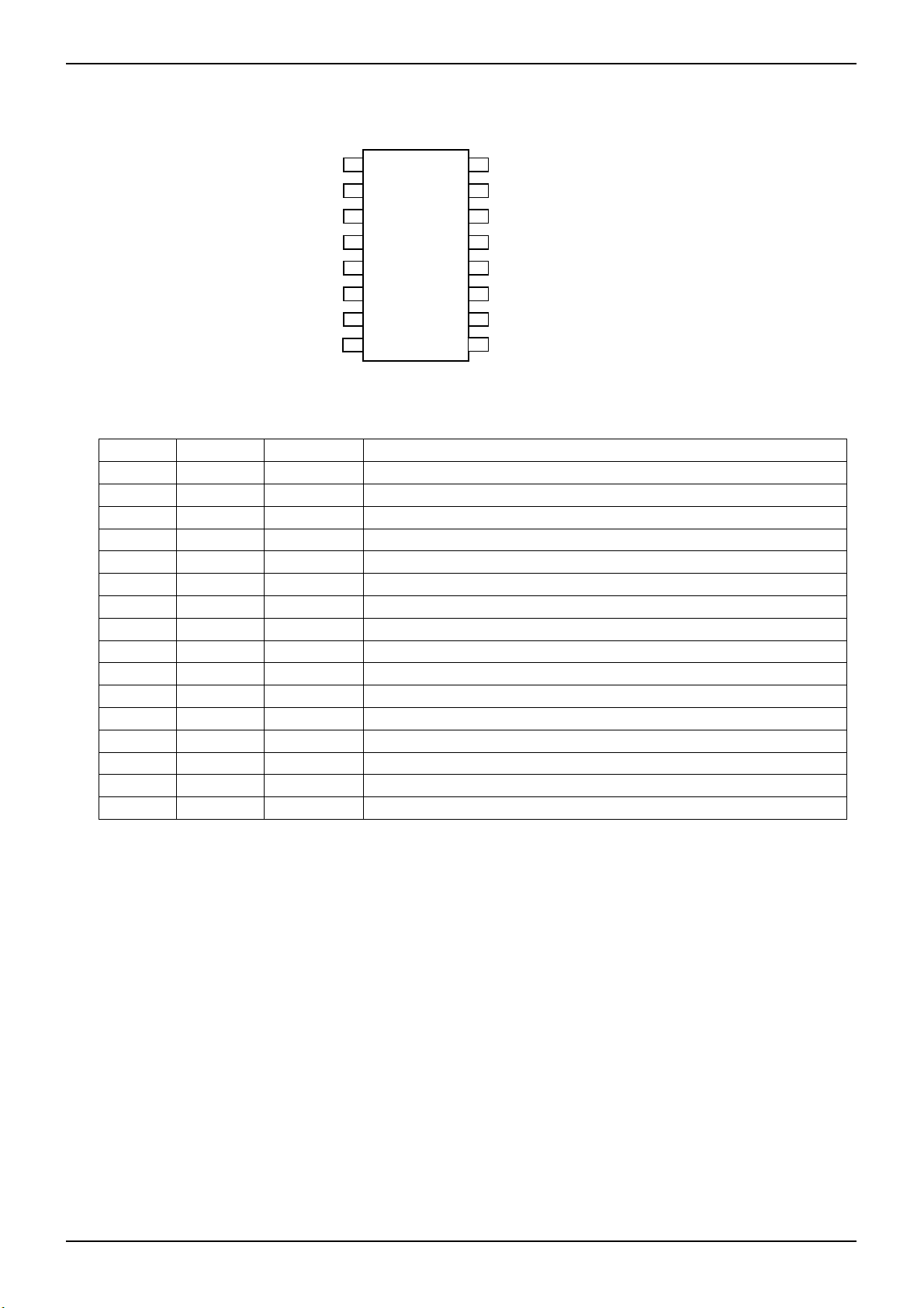
●Pin configuration
●PIN NAME
PIN No. PIN NAME I/O FUNCTIONS
1 VCC1 - Power Supply
2 SCL1 Input Serial clock input
3 SDA1 Input /output Slave and word address, Serial data input serial data output
4 WPB Input Write protect terminal(1 : Write enable, 0 : Write disable)
5 VCC OUT - Terminal of diode. Connect Bypass capacitor.
6 SDA0 Input /output Slave and word address, Serial data input serial data output
7 SCL0 Input Serial clock input
8 VCC0 - Power Supply
9 VCC3 - Power Supply
10 SCL3 Input Serial clock input
11 SDA3 Input /output Slave and word address, Serial data input serial data output
12 GND - Reference voltage of all input / output
13 N.C - Non connect terminal. Don’t connect each other.
14 SDA2 Input /output Slave and word address, Serial data input serial data output
15 SCL2 Input Serial clock input
16 VCC2 - Power Supply
Vcc1
SCL1
SDA1
WPB
VCC OUT
SDA0
SCL0
Vcc0
1
2
3
4
BU9883FV-W
5
6
7
8
Fig.37 Pin configuration
16
15
14
12
10
13
11
Technical Note
Vcc2
SCL2
SDA2
N.C
GND
SDA3
SCL3
Vcc3
9
www.rohm.com
© 2009 ROHM Co., Ltd. All rights reserved.
6/18
2009.04 - Rev.B

BU9883FV-W
●BLOCK DIAGRAM
Vcc1
Vcc2
Vcc3
Port 1
SCL1
SDA1
Port 2
SCL2
SDA2
Port 3
SCL3
SDA3
HDMI Sink
PWR_HDMI1
DDC_SCL1
DDC_SDA1
PWR_HDMI2
DDC_SCL2
DDC_SDA2
PWR_HDMI3
DDC_SCL3
DDC_SDA3
47KΩ
47KΩ
47KΩ
EN
EN
EN
I/O
(PORT1)
I/O
(PORT2)
I/O
(PORT3)
0.1uF
0.1uF
0.1uF
47KΩ
47KΩ
47KΩ
LEVEL
Shifter
LEVEL
Shifter
LEVEL
Shifter
Vcc1
SCL1
SDA1
Vcc2
SCL2
SDA2
Vcc3
SCL3
SDA3
SDA3
SCL3
SDA2
SCL2
SDA1
SCL1
Voltage
Detect
Logic
CONTROL
CONTROL
CONTROL
RD
RD
RD
BANK0
(2Kbit EEPROM)
BANK1
(2Kbit EEPROM)
BANK2
(2Kbit EEPROM)
WR
RD
WR
RD
WR
RD
Fig.38 BLOCK DIAGRAM
Vcc0
ROHM
Vcc OUT
BU9883FV-W
SCL_SINK
HDMI
Switch
SDA_SINK
WPB
SCL0
SDA0
GND
0.1uF
0.1uF
Fig.39 Application circuit
LDO
CONTROL
Low Voltage
Logic
LEVEL
Shifter
PWR_SYS
DDC_SCL
DDC_SDA
I/O
(PORT0)
μ Controller
WPB_OUT
2
I
C_SCL
2
C_SDA
I
HDMI
Receiver
SCL0
SDA0
EN
Technical Note
Vcc0
VCC OUT
WPB
Port 0
SCL0
SDA0
www.rohm.com
© 2009 ROHM Co., Ltd. All rights reserved.
7/18
2009.04 - Rev.B

BU9883FV-W
t
Technical Note
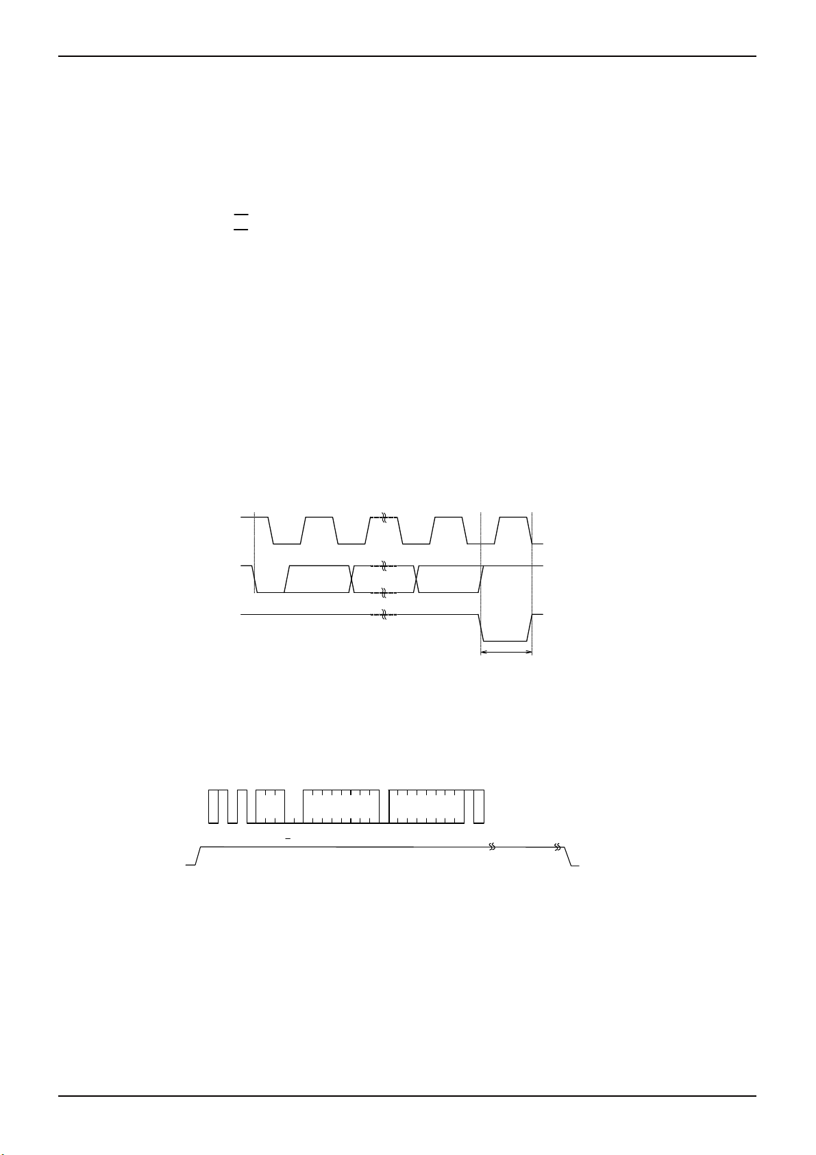
●WRITE CYCLE TIMING
SCL0
SDA0
D0 ACK
WRITE DATA(n)
STOP CONDITION START CONDITION
Fig.40 WRITE CYCLE TIMING
WR
●WRITE OPERATION
BU9883FV-W has 2K bit EEPROM in each port, there are three BANKs, 6K bit EEPROM in this device.
Each BANK EEPROM can be written through PORT0.
There is no write operation through PORT1,2,3.
When this device is accessed throgh PORT0, WPB terminal must be set to “HIGH”.
Table1 Access port and write enable BANK
Port0 BANK1~3
Port1 No write operation
Port2 No write operation
Port3 No write operation
●READ OPERATION
Each BANK EEPROM can be read through each port.
The relation ship of access port and access BANK is describe Table2.
Table 2 Table 3
Port0 BANK1~3 Port0 BANK1~3
Port1 No write operation Port1 BANK1
Port2 No write operation Port2 BANK2
Port3 No write operation Port3 BANK3
○When EEPROM access through PORT0, P1, P0 bits in slave address appoint access BANK.
Table 4
P1 P0 P1,P0 bit and access BANK
0 0 No bank selected
0 1 BANK1
1 0 BANK2
1 1 BANK3
Note) When P1=0, P0=0 : this device doesn’t return Acknowlege.
○During PORT0 access, WPB terminal must be set to “HIGH”, then PORT1~3 accesses will be cancelled.
○In accessing from PORT1~3, set WPB termianl to “LOW”
●DEVICE OPERATION
○START CONDITION
・All commands are proceeded by the start condition, which is a HIGH to LOW transition of SDA0~3 when SCL0~3 is
HIGH.
・This device continuously monitors the SDA0~3 and SCL0~3 lines for the start condition and will not respond to any
command until this condition has been met.
○STOP CONDITION
・All communications must be terminated by a stop condition, which is a LOW to HIGH transition of SDA0~3when SCL0
~3 is HIGH.
・The stop condition initiates internal write cycle to write the data into memory array after write sequence.
・The stop condition is also used to place the device into the standby power mode after read sequence.
・A stop condition can only be issued after the transmitting device has released the bus.
○NOTICE ON WRITE COMMAND
・In Write command, after transmit write data, if there are no stop condition, EEPROM data don’t change.
www.rohm.com
© 2009 ROHM Co., Ltd. All rights reserved.
8/18
2009.04 - Rev.B
BU9883FV-W
Technical Note
○DEVICE ADDRESSING
・Following a START condition, the master output the device address of the slave to be accessed.
The most significant four bits of the slave address are the “device type indentifier,” for this device, this is fixed as “1010.”
The next three bit specify a particular device. For PORT0 access, that are set “0”, “P1”, “P0”, for PORT 1~3 access, that
must be set “000”.
The last bit of the stream determines the operation to be performed.
When set to “1” a read operation is selected ; when set to “0,” a write operation is selected.
R/W set to “0” ・ ・ ・ ・ ・ ・ ・ ・ WRITE
R/W set to “1” ・ ・ ・ ・ ・ ・ ・ ・ READ
○ACKNOWLEDGE
・Acknowledge is a software convention used to indicate successful data transfers.The master or the slave will release the
bus after transmitting eight bits.During the ninth clock cycle, the receiver will pull the SDA line LOW to Acknowledgethat
the eight bits of data has been received.
・This device will respond with an Acknowledge after recognition of a START condition and its slave address.If both the
device and a write operation have been selected, this device will respond with an Acknowledge, after the receipt of each
subsequent 8-bit word.
・In the READ mode, this device will transmit eight bit of data, release the SDA line, and monitor the line for an
Acknowledge.
・If an Acknowledge is detected, and no STOP condition is generated by the master, this device will continue to transmit
the data.
・If an Acknowledge is not detected, this device will terminate further data transmissions and await a STOP condition
before returning to the standby mode.
・This device dosen't return Acknouwedge in internal write cycle.
SCL
(Fromμ-COM)
START CONDITION
(START BIT)
1 8 9
SDA
(μ-COM
OUTPUT DATA)
SDA
(IC OUTPUT DATA)
●PORT0 access commands
○For PORT0 access, WPB terminal must be set to “HIGH”.
○This write commands operate EEPROM write sequence at address which is appointed by P1, P0. When the master
generates a STOP condition, this device begins the internal write cycle to the nonvolatile array.
Fig.41 ACKNOWLEDGE RESPONSE FROM RECEIVER
S
T
A
SLAVE
R
ADDRESS
T
SDA
LINE
1 1 0 0
WPB
W
R
I
1st WORD
T
P1
P0
0
ADDRESS(n)
E
WA7
R
A
/
C
W
K
WA0
DATA(n)
D7
Fig.42 BYTE WRITE CYCLE TIMING (PORT0)
Acknowledge Signal
S
T
O
P
D0
A
C
K
(ACK Signal)
www.rohm.com
© 2009 ROHM Co., Ltd. All rights reserved.
9/18
2009.04 - Rev.B

BU9883FV-W
Technical Note
SDA
LINE
WPB
S
T
A
SLAVE
R
ADDRESS
T
1 1 0 0
W
R
I
T
E
P1
P0
0
R
/
W
1st WORD
ADDRESS(n)
WA7
A
C
K
WA0
DATA(n)
D7
A
C
K
D0
DATA(n+7)
A
C
K
S
T
O
P
D0
A
C
K
Fig.43 PAGE WRITE CYCLE TIMING (PORT0)
○This device is capable of eight byte page write operation.
○After the receipt of each word, the three low order address bits are internally incremented by one. The most
significant address bits (WA7~WA3) remain constant, if the master transmits more than 8 words.
○The relationship of P1, P0 inputs and access BANK is described as follows.
P1 P0 BANK
0 0 No opearation
0 1 BANK1
1 0 BANK2
1 1 BANK3
○Don't set P1, P0=0, 0. If P1, P0 are set to 0, there is no target bank, so this device doesn't return cknowlege.
○WPB terminal must be set to “HIGH” during Byte Write cycle, and Page Write cycle, and internal Write cycles. If WPB is
set to “LOW” in above condition, programing doesn't work, and during internal Write cycle, WPB terminal set to “LOW”,
this device terminate programing, and the data in programing address is not stored correctly.
S
T
A
SLAVE
R
ADDRESS
T
SDA
LINE
1 1 0 0
WPB
W
R
I
1st WORD
T
P1
P0
0
ADDRESS(n)
E
WA7
R
A
/
C
W
K
WA0
S
T
A
R
T
A
C
K
SLAVE
ADDRESS
1100
R
E
A
P0
P1
0
DATA(n)
D
D7
R
A
/
C
W
K
S
T
O
P
D0
A
C
K
○Random read operation allows the master to access any memory location which is appointed by P1, P0 bit.
This operation involves a two-step process.
First, the master issue a write command which includes the start condition and the slave address field (with R/W set to “0”)
followed by the address of the word be read.
This procedure sets the internal address counter of this device to the desired address. After the word address
acknowledge is received by the master, the master immediately reissues a start condition followed by the slave address
field with R/W the set to “1.” This device will respond with an acknowledge and then transmit the 8-data bits stored at the
addressed location.
If the master does not acknowledge the transmission but does generate the stop condition, at this point this device
discontinues transmission.
Fig.44 RANDOM READ CYCLE TIMING(PORT0)
SDA
LINE
WPB
S
T
A
R
T
SLAVE
ADDRESS
0 1 1 0 0
P1
P0
R
E
A
D
R
A
/
C
W
K
DATA
D7
D0
Fig.45 CURRENT READ CYCLE TIMING(PORT0)
S
T
O
P
A
C
K
www.rohm.com
© 2009 ROHM Co., Ltd. All rights reserved.
10/18
2009.04 - Rev.B

BU9883FV-W
S
0
Technical Note
○When the command just before Current Read cycle is Random Read cycle or Current Read cycle (each including
Sequential Read cycle), data of incremented last read address (n)-th address, i.e.n, data of the (n+1)-th address is output.
When the command just before Current Read cycle is Byte Write or Page write, data of latest write address is output.
○Current Read operation allows the master to access data word stored in internal address counter which is appointed by
P1, P0 bit. This operation involves a two-step process. This device will respond with an acknowledge and then transmit
the 8-data bits stored at the addressed location.
If the master does not acknowledge the transmission but does generate the stop condition, at this point this device
discontinues transmission.
note)If the master send Acknowredge at after D0 output, Sequential Read is selected, and this device output next address
data, and master can't send stop condition, so master can't discontinues transmission.
To stop read command, the master must send no Acknowledge at after D0 output, and issue stop condition.
SDA
LIN
S
T
A
R
T
1 1 0 0
SLAVE
ADDRES
R
E
A
D
P10
P0
DATA(n)
D7
S
DATA(n+x)
D
D7
T
O
P
D0
WPB
Fig.46 SEQUENTIAL READ CYCLE TIMING (PORT0)
○During the sequential read operation, the internal address counter of this device automatically increments with each
acknowledge received ensuring the data from address will be followed with the data from n+1. For read operations, all bits
of the address counter are incremented allowing the entire array to be read during a single operation. When the counter
reaches the top of the array, it will “roll over” to the bottom of the array of BANK and continue to transmit the data.
○The sequential read operation can be performed with both current read and random read.
●PORT1,2,3 access commands
S
T
A
SLAVE
R
ADDRESS
T
SDA
LINE
1 1 0 0
WPB
W
R
I
1st WORD
T
0 0
0
ADDRESS(n)
E
WA7
R
A
/
C
W
K
S
T
A
SLAVE
R
ADDRESS
T
WA0
1 1 0 0
A
C
K
R
E
A
0
0
0
R
/
W
DATA(n)
D
D7
A
C
K
S
T
O
P
D0
A
C
K
Fig.47 RANDOM READ CYCLE TIMING(PORT1~3)
○Random read operation allows the master to access any memory location of the BANK which is appointed by P1, P0. This
operation involves a two-step process.
First, the master issues a write command which includes the start condition and the slave address field (with R/W set to
“0”) followed by the address of the word be read.
This procedure sets the internal address counter of this device to the desired address.
After the word address acknowledge is received by the master, the master immediately reissues a start condition followed
by the slave address field with R/W the set to “1.”
This device will respond with an acknowledge and then transmit the 8-data bits stored at the addressed location. If the
master does not acknowledge the transmission but does generate the stop condition, at this point this device discontinues
transmission.
S
T
A
SLAVE
R
ADDRESS
T
SDA
LINE
WPB
R
E
A
D
01 10 0
00
R
A
/
C
W
K
DATA
D7
S
T
O
P
D0
A
C
K
Fig.48 CURRENT READ CYCLE TIMING(PORT1~3)
www.rohm.com
© 2009 ROHM Co., Ltd. All rights reserved.
11/ 18
2009.04 - Rev.B

BU9883FV-W
Technical Note
○When the command just before Current Read cycle is Random Read cycle or Current Read cycle (each including
Sequential Read cycle), data of incremented last read address (n)-th address, i.e.n, data of the (n+1)-th address is output.
When the command just before Current Read cycle is Byte Write or Page write, data of latest write address is output.
○Random read operation allows the master to access any memory location. The BANK which is appointed by P1, P0. This
operation involves a two-step process.
First, the master issues a write command which includes the start condition and the slave address field (with R/W set to
“0”) followed by the address of the word be read. This procedure sets the internal address counter of this device to the
desired address. After the word address acknowledge is received by the master, the master immediately reissues a
start condition followed by the slave address field with R/W the set to “1.” This device will respond with an acknowledge
and then transmit the 8-data bits stored at the addressed location.
If the master does not acknowledge the transmission but does generate the stop condition, at this point this device
discontinues transmission.
note)If the master send Acknowredge at after D0 output, Sequential Read is selected, and this device output next address data, and master can't send stop
condition, so master can't discontinues transmission. To stop read command, the master must send no Acknowledge at after D0 output, and issue stop
condition.
S
T
A
SLAVE
R
ADDRESS
T
SDA
LINE
1 1 0 0
WPB
R
E
A
0 0
0 D0
R
※1
W
DATA(n)
D
D7
A
/
C
K
S
T
DATA(n+x)
D7
A
C
K
A
C
K
O
P
D0
A
C
K
Fig.49 SEQUENTIAL READ CYCLE TIMING (PORT1~3)
○During the sequential read operation, the internal address counter of this device automatically increments with each
acknowledge received ensuring the data from address n will be followed with the data from n+1. For read operations, all
bits of the address counter are incremented allowing the entire array to be read during a single operation. When the
counter reaches the top of the array, it will “roll over to the bottom of the array and continue to transmit the data.
○The sequential read operation can be performed with both current read and random read.
●Access Control of PORT0,1,2,3
WPB terminal controls access enable of each PORT, as follows.
PORT
PORT0 not accessible Read/Write
PORT1 Read not accessible
PORT2 Read not accessible
PORT3 Read not accessible
Table4 WPB terminal and port accesibility
○ When WPB terminal is “HIGH”, PORT0 only can access this device.
In this case, when commands from PORT1, 2, 3 are inputted, these port don't return acknowledge.
○ When WPB terminal is “LOW”, PORT0 access is not valid, but PORT1, 2, 3 can access this device this device.
Commands from PORT1, 2, 3 is performs independently other port.
WPB terminal inputs
0 1
www.rohm.com
© 2009 ROHM Co., Ltd. All rights reserved.
12/18
2009.04 - Rev.B

BU9883FV-W
A
A
A
A
A
A
Technical Note
●Software reset
Software reset is executed when to avoid malfunction after power on, and to reset during command input. Software reset
has several kinds, and 3 kinds of them are shown in the figure below. (Refer to Fig.50(a), Fig.50(b), and Fig.50 (c).) In
dummy clock input area, release the SDA0~3 bus ('H' by pull up). In dummy clock area, ACK output and read data '0' (both
'L' level) may be output from EEPROM, therefore, if 'H' is input forcibly, output may conflict and over current may flow,
leading to instantaneous power failure of system power source or influence upon devices.
SCL0~3
SDA0~3
Fig.50-(a) The case of dummy clock +START+START+ command input
Dummy clock×14
2 13
1
14
Star t×2
Normal command
Normal command
SCL0~3
SDA0~3
Fig.50-(b) The case of START +9 dummy clocks +START+ command input
SCL0~3
SDA0~3
Star t
1
Dummy clock×9
1
2
3
2
8
Star t×9
7
Fig.50-(c) START×9+ command input
Star t
9
8
9
*Start command from START input.
Normal command
Normal command
Normal command
Normal command
●Acknowledge polling
During internal write execution, all input commands are ignored, therefore ACK is not sent back. During internal automatic
write execution after write cycle input, next command (slave address) is sent, and if the first ACK signal sends back 'L', then
it means end of write action, while if it sends back 'H', it means now in writing. By use of acknowledge polling, next
command can be executed without waiting for tWR = 5ms.
When to write continuously, R/W = 0, when to carry out current read cycle after write, slave address R/W = 1 is sent, and if
ACK signal sends back 'L', then execute word address input and data output and so forth.
First write command
During internal write,
ACK = HIGH is sent back.
S
T
A
Write command
R
T
S
S
T
A
R
T
Slave
address
T
O
P
S
T
A
R
T
Slave
address
C
K
H
C
K
H
tWR
Second write command
…
S
T
A
R
T
Slave
address
t
WR
C
K
H
S
T
Slave
A
address
R
T
Word
C
K
address
L
After completion of internal write,
ACK=LOW is sent back, so input next
word address and data in succession.
C
Data
K
L
S
T
C
O
K
P
L
Fig.51 Case to continuously write by acknowledge polling
www.rohm.com
© 2009 ROHM Co., Ltd. All rights reserved.
13/18
2009.04 - Rev.B

BU9883FV-W
Technical Note
●Command cancel by start condition and stop condition
During command input, by continuously inputting start condition and stop condition, command can be cancelled.
(Refer to Fig. 52.)
However, in ACK output area and during data read, SDA0~3 bus may output 'L', and in this case, start condition and stop
condition cannot be input, so reset is not available. Therefore, execute software reset. And when command is cancelled by
start, stop condition, during random read cycle, sequential read cycle, or current read cycle, internal setting address is not
determined, therefore, it is not possible to carry out current read cycle in succession. When to carry out read cycle in
succession, carry out random read cycle.
SCL0~3
SDA0~3
1 1
0 0
●I/O peripheral circuit
Fig.52 Case of cancel by start, stop condition during slave address input
Start condition Stop condition
○Pull up resistance of SDA0~3 terminal
SDA0~3 is NMOS open drain, so requires pull up resistance. As for this resistance value (RPU), select an appropriate
value to this resistance value from microcontroller VIL, IL, and VOL0~3-IOL characteristics of this IC. If RPU is large,
action frequency is limited. The smaller the RPU, the larger the consumption current at action.
○Maximum value of R
PU
The maximum value of RPU is determined by the following factors. The following VCC, SDA, RPU and IL correspond to them
of each port.
(1)SDA0~3 rise time to be determined by the capacitance (CBUS) of bus line of R
and SDA0~3 should be tR or below.
PU
And AC timing should be satisfied even when SDA0~3 rise time is late.
(2)The bus electric potential ○A to be determined by input leak total (IL) of device connected to bus at output of 'H' to
SDA0~3 bus and R
should sufficiently secure the input 'H' level (VIH) of microcontroller and EEPROM including
PU
recommended noise margin 0.2VCC.
Vcc - ILR
Ex. ) When V
○Minimum value of R
- 0.2Vcc ≧ VIH
PU
∴ R
PU
=3V, IL=10μA, VIH=0.7 VCC,
CC
from (2)
R
PU
=
≦
PU
≦ 300 [kΩ]
0.8Vcc-V
IH
I
L
0.8×3-0.7×3
-6
10×10
マイコン
Microcontroller
RPU
IL
Bus line
バスライン容量
capacity
CBUS
CBUS
Fig.53 I/O circuit diagram
A
BU9883FV-W
SDA terminal
IL
The minimum value of RPU is determined by the following factors. The following VCC, VOL, IOL, and RPU correspond to
them of each port.
(1)When IC outputs LOW, it should be satisfied that V
(2)V
OLMAX
VCC-VOL
R
≦ I
OL
PU
=0.4V should secure the input 'L' level (VIL) of microcontroller and EEPROM including recommended noise
∴ R
PU
OLMAX
≦
=0.4V and I
VC-V
OL
I
OL
OLMAX
=3mA.
margin 0.1VCC.
V
≦ VIL-0.1 VCC
OLMAX
Ex. ) When VCC =3V, V
from (1)
R
PU
And
V
OL
V
IL
=0.4V, IOL=3mA, microcontroller, EEPROM VIL=0.3VCC
OL
3-0.4
≧
3×10
-3
≧ 867 [Ω]
= 0.4 [V]
= 0.3×3
= 0.9 [V]
Therefore, the condition (2) is satisfied.
○Pull up resistance of SCL0~3 terminal
When SCL0~3 control is made at CMOS output port, there is no need, but in the case there is timing where SCL0~3
becomes 'Hi-Z', add a pull up resistance. As for the pull up resistance, one of several kΩ ~ several ten kΩ is recommended
in consideration of drive performance of output port of microcontroller.
www.rohm.com
© 2009 ROHM Co., Ltd. All rights reserved.
14/18
2009.04 - Rev.B

BU9883FV-W
A
A
Technical Note
●Cautions on microcontroller connection
○Rs
In I2C BUS, it is recommended that SDA port is of open drain input/output. However, when to use CMOS input / output of
tri state to SDA port, insert a series resistance Rs between the pull up resistance Rpu and the SDA terminal of EEPROM.
This is controls over current that occurs when PMOS of the microcontroller and NMOS of EEPROM are turned ON
simultaneously. Rs also plays the role of protection of SDA terminal against surge. Therefore, even when SDA port is
open drain input/output, Rs can be used. The following SCL SDA RPU and R
correspond to them of each port.
S
CK
RPU
RS
SCL
SDA
'H' output of microcontroller
'L' output of EEPROM
Microcontroller
EEPROM
Fig.54 I/O circuit diagram
Over current flows to SDA line by 'H'
output of microcontroller and 'L'
output of EEPROM.
Fig.55 Input / output collision timing
○Maximum value of Rs
The maximum value of Rs is determined by the following relations. The following VCC, V
, RS, RPU, IOL, and SDA
OL
correspond to them of each port.
(1)SDA rise time to be determined by the capacity (CBUS) of bus line of Rpu and SDA should be tR or below.
And AC timing should be satisfied even when SDA rise time is late.
(2)The bus electric potential
sufficiently secure the input 'L' level (V
VIL
Microcontroller
Fig.56 I/O circuit diagram
○Minimum value of Rs
The minimum value of Rs is determined by over current at bus collision. When over current flows, noises in power source
line, and instantaneous power failure of power source may occur. When allowable over current is defined as I, the
following relation must be satisfied. Determine the allowable current in consideration of impedance of power source line in
set and so forth. Set the over current to EEPROM 10mA or below. The following VCC, RPU, RS, and I correspond to them
of each port.
A to be determined by Rpu and Rs the moment when EEPROM outputs 'L' to SDA bus should
VCC
RPU
Bus line
capacity CBUS
○
R
IOL
S
) of microcontroller including recommended noise margin 0.1VCC.
IL
VOL
EEPROM
Example
from(2),
(V
CC
∴
When VCC=3V, VIL=0.3V
)
V
-
R
PU+RS
R
S
R
S
)×R
OL
S
V
IL
≦
≦
-
1.1V
0.3×3-0.4-0.1×3
1.1×3-0.3×3
+VOL+0.1V
V
0.1V
OL
CC
-
CC,
-
CC
V
IL
V
OL
CC
=0.4V, RPU=20kΩ,
≦
V
×
×
1.67[kΩ
≦
]
IL
R
'H' output
Microcontroller
Fig.57 I/O circuit diagram
R
PU
R
S
Over currentⅠ
'L' output
EEPROM
V
CC
≦
R
S
R
S
∴
≧
Example)When V
I
V
CC
I
=3V, I=10mA
CC
R
S
≧
≧
10×10
300
3
-3
[Ω]
PU
20×10
3
www.rohm.com
© 2009 ROHM Co., Ltd. All rights reserved.
15/18
2009.04 - Rev.B

BU9883FV-W
Technical Note
●I2C BUS input / output circuit
○Input (SCL0~3)
Fig.58 Input pin circuit diagram
○Input / output (SDA0~3)
Fig.59 Input / output pin circuit diagram
○Input (WPB)
Fig.60 Input pin circuit diagram
●Notes on power ON
At power on, in IC internal circuit and set, VCC rises through unstable low voltage area, and IC inside is not completely reset,
and malfunction may occur. To prevent this, functions of POR circuit and LVCC circuit are equipped. To assure the action,
observe the following conditions at power on.
1. Set SDA0
2. Start power source so as to satisfy the recommended conditions of t
~3 = 'H' and SCL0~3 ='L' or 'H'
VCC
, t
, and Vbot for operating POR circuit.
R
OFF
t
R
Recommended conditions of tR, t
OFF
,Vbot
t
OFF
0
Fig.60 Rise waveform diagram
www.rohm.com
© 2009 ROHM Co., Ltd. All rights reserved.
t
R
Vbot
10ms or below 10ms or longer 0.3V or below
t
OFF
Vbot
100ms or below 10ms or longer 0.2V or below
16/18
2009.04 - Rev.B

BU9883FV-W
A
Technical Note
3. Set SDA0~3 and SCL0~3 so as not to become 'Hi-Z'.
When the above conditions 1 and 2 cannot be observed, take the following countermeasures.
a) In the case when the above condition 1 cannot be observed. When SDA0
→Control SCL0~3 and SDA0~3 as shown below, to make SCL0~3 and SDA0~3, 'H' and 'H'.
V
CC
SCL
t
LOW
~3 becomes 'L' at power on.
SDA
fter Vcc becomes stable
t
t
SU:DAT
DH
Fig.61 When SCL0~3= 'H' and SDA0~3= 'L'
After Vcc becomes stable
Fig.62 When SCL0
t
SU:DAT
~3='L' and SDA0~3='L'
b) In the case when the above condition 2 cannot be observed.
→After power source becomes stable, execute software reset(P11).
c) In the case when the above conditions 1 and 2 cannot be observed.
→Carry out a), and then carry out b).
●Low voltage malfunction prevention function
LVCC circuit prevents data rewrite action at low power, and prevents wrong write. At LVCC voltage (Typ. =1.2V) or below, it
prevent data rewrite.
●VCC noise countermeasures
Bypass capacitor
○
When noise or surge gets in the power source line, malfunction may occur, therefore, for removing these, it is
recommended to attach a by pass capacitor (0.1μF) between IC VCC
as possible. And, it is also recommended to attach a bypass capacitor between board VCC
OUT and GND. At that moment, attach it as close to IC
OUT and GND.
●Cautions on use
(1) Described numeric values and data are design representative values, and the values are not guaranteed.
(2) We believe that application circuit examples are recommendable, however, in actual use, confirm characteristics further
sufficiently. In the case of use by changing the fixed number of external parts, make your decision with sufficient margin
in consideration of static characteristics and transition characteristics and fluctuations of external parts and our LSI.
(3) Absolute maximum ratings
If the absolute maximum ratings such as impressed voltage and action temperature range and so forth are exceeded,
LSI may be destructed. Do not impress voltage and temperature exceeding the absolute maximum ratings. In the case
of fear exceeding the absolute maximum ratings, take physical safety countermeasures such as fuses, and see to it that
conditions exceeding the absolute maximum ratings should not be impressed to LSI.
(4) GND electric potential
Set the voltage of GND terminal lowest at any action condition. Make sure that each terminal voltage is lower than that of
GND terminal.
(5) Terminal design
In consideration of permissible loss in actual use condition, carry out heat design with sufficient margin.
(6) Terminal to terminal shortcircuit and wrong packaging
When to package LSI onto a board, pay sufficient attention to LSI direction and displacement. Wrong packaging may
destruct LSI. And in the case of shortcircuit between LSI terminals and terminals and power source, terminal and GND
owing to foreign matter, LSI may be destructed.
(7) Use in a strong electromagnetic field may cause malfunction, therefore, evaluate design sufficiently.
www.rohm.com
© 2009 ROHM Co., Ltd. All rights reserved.
17/18
2009.04 - Rev.B

BU9883FV-W
●Ordering part number
B U 9 8 8 3 F V - W E 2
Technical Note
Part No. Part No.
SSOP-B16
5.0±0.2
16
4.4±0.2
6.4±0.3
1
1.15±0.1
0.10
0.65
9
0.3Min.
8
0.15±0.1
0.1
0.22±0.1
(Unit : mm)
<Tape and Reel information>
Package
FV: SSOP-B16
Embossed carrier tapeTape
Quantity
Direction
of feed
2500pcs
E2
The direction is the 1pin of product is at the upper left when you hold
()
reel on the left hand and you pull out the tape on the right hand
Reel
W: Double Cell
Packaging and forming specification
E2: Embossed tape and reel
1pin
Order quantity needs to be multiple of the minimum quantity.
∗
Direction of feed
www.rohm.com
© 2009 ROHM Co., Ltd. All rights reserved.
18/18
2009.04 - Rev.B

Notes
No copying or reproduction of this document, in part or in whole, is permitted without the
consent of ROHM Co.,Ltd.
The content specied herein is subject to change for improvement without notice.
The content specied herein is for the purpose of introducing ROHM's products (hereinafter
"Products"). If you wish to use any such Product, please be sure to refer to the specications,
which can be obtained from ROHM upon request.
Examples of application circuits, circuit constants and any other information contained herein
illustrate the standard usage and operations of the Products. The peripheral conditions must
be taken into account when designing circuits for mass production.
Great care was taken in ensuring the accuracy of the information specied in this document.
However, should you incur any damage arising from any inaccuracy or misprint of such
information, ROHM shall bear no responsibility for such damage.
The technical information specied herein is intended only to show the typical functions of and
examples of application circuits for the Products. ROHM does not grant you, explicitly or
implicitly, any license to use or exercise intellectual property or other rights held by ROHM and
other par ties. ROHM shall bear no responsibility whatsoever for any dispute arising from the
use of such technical information.
Notice
The Products specied in this document are intended to be used with general-use electronic
equipment or devices (such as audio visual equipment, ofce-automation equipment, communication devices, electronic appliances and amusement devices).
The Products specied in this document are not designed to be radiation tolerant.
While ROHM always makes efforts to enhance the quality and reliability of its Products, a
Product may fail or malfunction for a variety of reasons.
Please be sure to implement in your equipment using the Products safety measures to guard
against the possibility of physical injury, re or any other damage caused in the event of the
failure of any Product, such as derating, redundancy, re control and fail-safe designs. ROHM
shall bear no responsibility whatsoever for your use of any Product outside of the prescribed
scope or not in accordance with the instruction manual.
The Products are not designed or manufactured to be used with any equipment, device or
system which requires an extremely high level of reliability the failure or malfunction of which
may result in a direct threat to human life or create a risk of human injur y (such as a medical
instrument, transportation equipment, aerospace machinery, nuclear-reactor controller,
fuel-controller or other safety device). ROHM shall bear no responsibility in any way for use of
any of the Products for the above special purposes. If a Product is intended to be used for any
such special purpose, please contact a ROHM sales representative before purchasing.
If you intend to export or ship overseas any Product or technology specied herein that may
be controlled under the Foreign Exchange and the Foreign Trade Law, you will be required to
obtain a license or permit under the Law.
Thank you for your accessing to ROHM product informations.
More detail product informations and catalogs are available, please contact us.
ROHM Customer Support System
www.rohm.com
© 2009 ROHM Co., Ltd. All rights reserved.
http://www.rohm.com/contact/
R0039
A
 Loading...