ROHM BU9877FV Datasheet

•
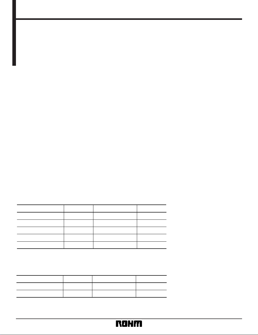
Absolute maximum ratings (Ta = 25°C)
Applied voltage
Power dissipation
Storage temperature
Operating temperature
Input voltage
Pd
∗
1 Reduced by 3.0mW for each increase in Ta of 1°C over 25°C.
VCC
Parameter Symbol
Tstg
Topr
—
– 0.3 ~ + 7.0
Limits
– 65 ~ + 125
– 40 ~ + 85
– 0.3 ~ V
CC + 0.3
mW
V
Unit
°C
°C
V
300
∗
•
Applications
168-pin and 144-pin DRAM modules containing synchronous DRAM
•
Features
1) 2-k bit EEPROM with configuration of 256 words × 8
bits.
2) Compliance with SPD data format.
3) Dual-line serial (I
2
C bus) interface.
4) Protective functions enabled by a one-time ROM
and write protect pin.
Soft ware protection. as a one-time ROM: 00 to 7Fh.
Hard ware protection (WP pin): 80 to FFh.
5) Compact SSOP-B 8-pin package.
1
Memory ICs
Serial interface IC for DIMMs supporting plug & play
BU9877FV
The BU9877FV is a 2-k bit EEPROM with a write protect function, developed for DIMMs (Dual In-line Memory
Modules) containing a synchronous DRAM. This IC stores IDs in memory in order to enable Plug & Play functions.
•
Recommended operating conditions (Ta = 25°C)
Power supply voltage
Input voltage V
IN
VCC
Parameter Symbol
V
V
Unit
2.7 ~ 5.5
Limits
0 ~ V
CC

2
Memory ICs BU9877FV
•
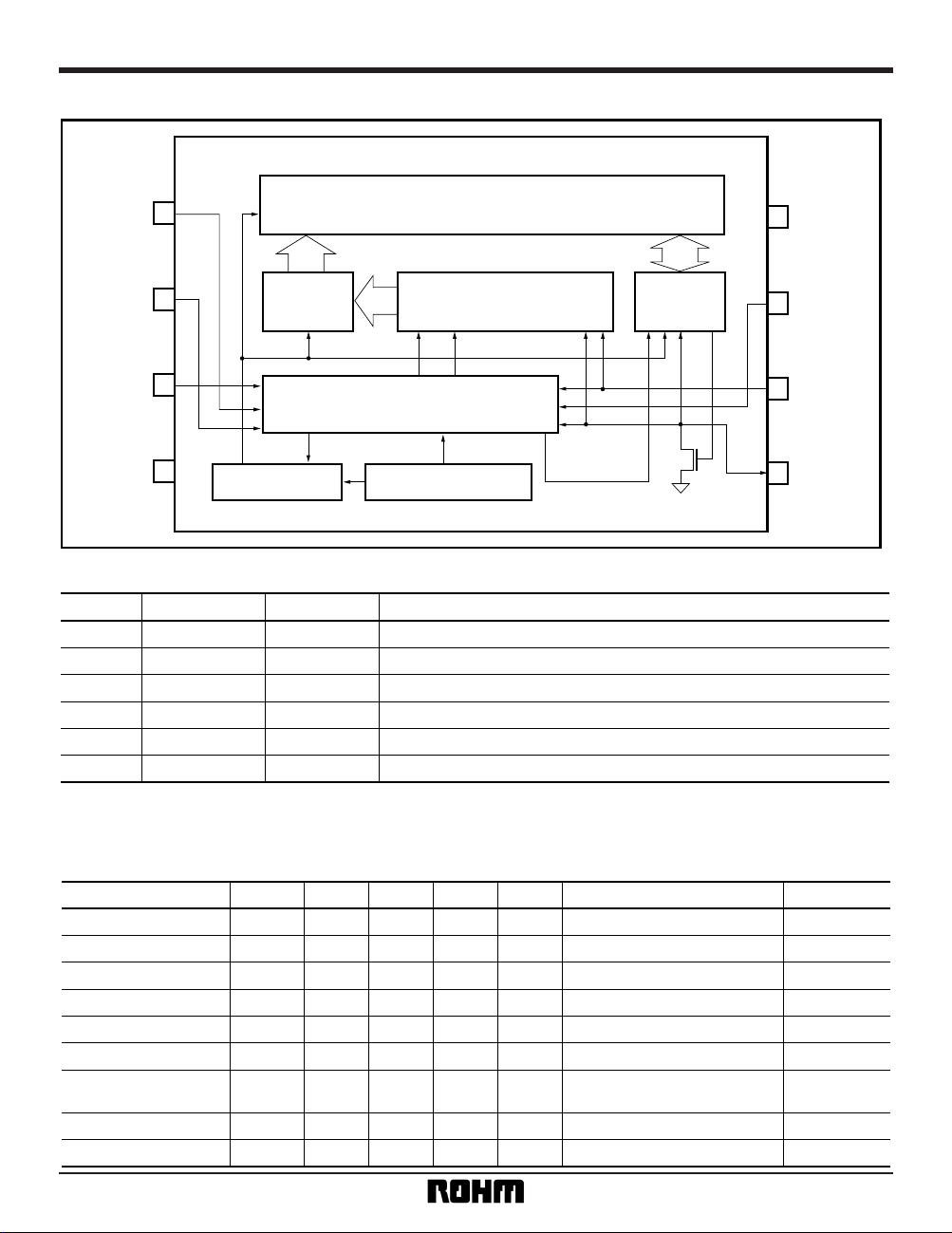
Block diagram
1
2
3
4
8
Vcc
A0
A1
A2
GND
WP
SCL
SDA
7
6
5
2048bit EEPROM Array
8bit
8bit
8bit
Address
Decoder
Slave · word
Address Register
Data
Register
START
STOP
Control Circuit
Write Protect Control Circuit
ACK
High voltage generator
Power supply voltage detector
•
Pin descriptions
Note: The SDA pin is Nch open drain output, and should be used with external pull-up resistor.
The WP pin is equipped with internal pull-down resistor, so can be left open when used.
Slave address setting (pin)
Input / output reference voltage of 0V
Slave and word address, serial data input / output
Serial clock input
Write protect input
Connect the power supply to this.
Pin name
Pin No.
Function
I / O
A0, A1, A2
1, 2, 3 I
GND
4—
SDA
5 I / O
SCL
6I
WP
7I
V
CC
8—
•
Electrical characteristics (unless otherwise noted, Ta = – 40 to + 85°C, Vcc = 2.7V to 5.5V)
VIH
Input high level voltage —
V
V
IL
Input low level voltage
0.3V
CC V
V
OL
Output low level voltage
I
OL = 3.0mA (SDA)
Fig.10.4 V
I
LI1
Input leakage current 1 VIN = 0V ~ VCC
Fig.21
µA
I
LI2
Input leakage current 2 VIN = 0V ~ VCC (WP)
Fig.220
µA
I
LO
Output leakage current VOUT = 0V ~ VCC
Fig.21
µA
I
CC
Operating current
consumption
V
CC = 5.5V, fSCL = 100kHz
Fig.3
3.0 mA
I
SB
Standby current VCC = 5.5V, SDA · SCL = VCC
Fig.42.0
µA
f
SCL
SCL frequency
100 kHz
Parameter Symbol
Measurement circuit
0.7VCC
—
—
– 1
– 1
– 1
—
—
—
Min.
—
—
—
—
—
—
—
—
—
Typ. Max. Unit Conditions
—
—
—
—
—
—

3
Memory ICs BU9877FV
•
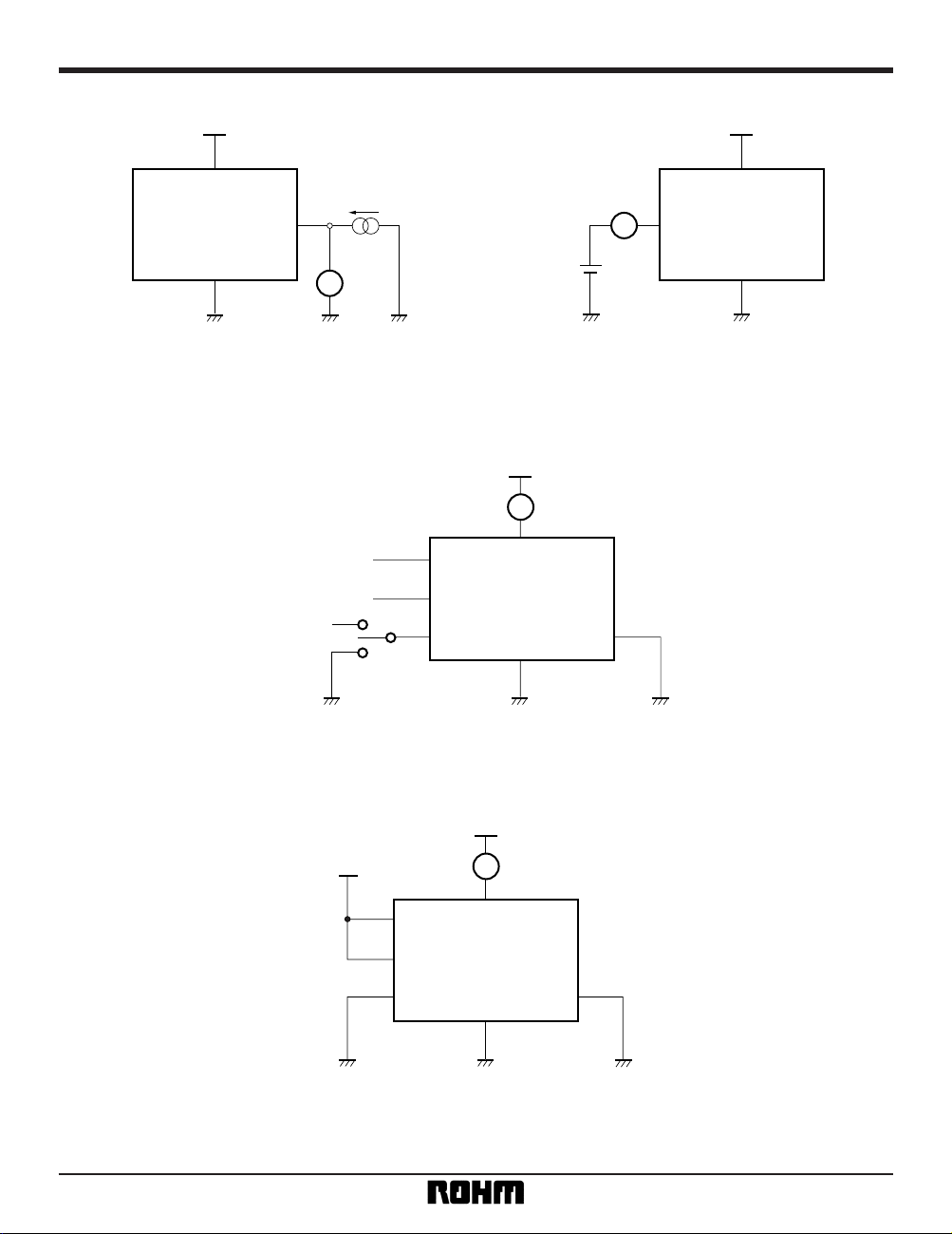
Measurement circuits
VCC
VCC
VOL
Data set when output is LOW
3.0mA
GND
V
SDA
Fig. 1 LOW output voltage measurement circuit
VCC
VOUT = 0 ~ VCC
VIN = 0 ~ VCC
ILO
ILI
VCC
GND
A
A0, A1, A2
SDA, SCL, WP
Fig. 2 Input / output leakage current measurement circuit
VCC
ICC
VCC
VCC
GND
A
SDA
WP
SCL
100kHz clock
Write / read input
A0, A1, A2
Fig. 3 Current consumption measurement circuit
VCC
VCC
ISB
VCC
GND
A
SDA
WP
SCL
A0, A1, A2
Fig. 4 Standby current measurement circuit
 Loading...