

A
High Reliability Series Serial EEPROMs
WL-CSP EEPROM family
I2C BUS
BU9833GUL-W
●Description
BU9833GUL-W series is a serial EEPROM of I
available at 400kHz.
●Features
1) Completely conforming to the world standard I
and serial data(SDA)
2) Other devices than EEPROM can be connected to the same port, saving microcontroller port.
3) Actions available at 400kHz clock (1.7V~5.5V)
4) 1.7~5.5V single power source action most suitable for battery use.
5) Page write mode useful for initial value write at factory shipment.
6) Auto erase and auto end function at data rewrite.
7) Low current consumption
At write action (5V) : 1.2mA (Typ.)
At read action (5V) : 0.2mA (Typ.)
At standby action (5V) : 0.1μA (Typ.)
8) Write mistake prevention function
Write (write protect) function added.
Write mistake prevention function at low voltage.
9) Data rewrite up to 1,000,000times.
10) Data kept for 40 years.
11) Noise filter built in SCL / SDA terminal
12) Shipment data all address FFh.
●Page write
2
C BUS interface method. 1.7V single power source action and actions
2
C BUS. All controls available by 2 ports of serial clock (SCL)
No.10001EAT17
Product number Number of pages
BU9833GUL-W 16Byte
●BU9833GUL-W
Type Capacity Bit format
BU9833GUL-W
●Absolute maximum ratings (Ta=25℃)
Parameter Symbol Ratings Unit
Impressed voltage Vcc
Permissible dissipation Pd 220 mW
Storage temperature range Tstg -65~125 ℃
Operating temperature range Topr -40~85 ℃
Terminal voltage – -0.3~Vcc+1.0 V
・When using at Ta=25℃ or higher, 2.2mW (*1) to be reduced per 1℃
2Kbit 256×8 1.7~5.5V VCSP50L1
-0.3~+6.5*1
Power source
voltage
V
Package
www.rohm.com
© 2010 ROHM Co., Ltd. All rights reserved.
1/18
2010.10 - Rev.
A
BU9833GUL-W
●Recommended action conditions
Parameter Symbol Ratings Unit
Power source voltage Vcc 1.7~5.5
Input voltage Vin 0~Vcc
●Memory cell characteristics (Ta=25℃, Vcc=1.7~5.5V)
Parameter
Number of data rewrite times
*1
1,000,000 - - Times
Min Typ. Max
Limits
Technical Note
V
Unit
Data hold years
*
1:Not 100% TESTED
*1
40 - - Years
●Electrical characteristics
(Unless otherwise specified, Ta=-40~+85℃, Vcc=1.7~5.5V)
Parameter Symbol
“HIGH” input voltage1 V
“LOW” Input voltage1 V
“HIGH” input voltage2 V
“LOW” input voltage2 V
“HIGH” input voltage3 V
“LOW” input voltage3 V
“LOW” output voltage1 V
“LOW output voltage2 V
Min. Typ. Max.
0.7Vcc - Vcc+1.0 V 2.5V≦Vcc≦5.5V
IH1
-0.3 - 0.3Vcc V 2.5V≦Vcc≦5.5V
IL1
0.8Vcc - Vcc+1.0 V 1.8V≦Vcc<2.5V
IH2
-0.3 - 0.2Vcc V 1.8V≦Vcc<2.5V
IL2
0.9Vcc - Vcc+1.0 V 1.7V≦Vcc<1.8V
IH3
-0.3 - 0.1Vcc V 1.7V≦Vcc<1.8V
IL3
- - 0.4 V IOL=3.0mA, 2.5V≦Vcc≦5.5V, (SDA)
OL1
- - 0.2 V IOL=0.7mA, 1.7V≦Vcc<2.5V, (SDA)
OL2
Limits
Unit Conditions
Input leak current ILI -1 - 1 μA VIN=0V~Vcc
Output leak current ILO -1 - 1 μA V
I
- - 2.0 mA
CC1
Current consumption at action
I
- - 0.5 mA
CC2
Standby current ISB - - 2.0 μA
○This product is not designed for protection against radioactive rays.
www.rohm.com
© 2010 ROHM Co., Ltd. All rights reserved.
2/18
=0V~Vcc(SDA)
OUT
Vcc=5.5V, f
=400kHz, tWR=5ms,
SCL
Byte write, Page write
Vcc=5.5V, f
=400kHz
SCL
Random read, vurrent read,
sequential read
Vcc=5.5V, SDA·SCL=Vcc,
A2=GND, WP=GND
2010.10 - Rev.
A
BU9833GUL-W
ACK
A
A
A
A
Technical Note
●Action timing Characteristics
(Unless otherwise specified, Ta=-40~+85℃,Vcc=1.7~5.5V)
FAST-MODE
Parameter Symbol
2.5V≦Vcc≦5.5V
STANDARD-MODE
2.5V≦Vcc≦5.5V
Min. Typ. Max. Min. Typ. Max.
SCL frequency fSCL - - 400 - - 100 kHz
Data clock “HIGH” time tHIGH 0.6 - - 4.0 - - μs
Data clock “LOW” time tLOW 1.2 - - 4.7 - - μs
SDA, SCL rise time *1 tR *1 - - 0.3 - - 1.0 μs
SDA< SCL fall time *1 tF *1 - - 0.3 - - 0.3 μs
Start condition hold time tHD:STA 0.6 - - 4.0 - - μs
Start condition setup time tSU:STA 0.6 - - 4.7 - - μs
Input data hold time tHD:DAT 0 - - 0 - - ns
Input data setup time tSU:DAT 100 - - 250 - - ns
Output data delay time tPD 0.1 - 0.9 0.2 - 3.5 μs
Output data hold time tDH 0.1 - - 0.2 - - μs
Stop condition setup time tSU:STO 0.6 - - 4.7 - - μs
Bus release time before transfer start tBUF 1.2 - - 4.7 - - μs
Internal write cycle time tWR - - 5 - - 5 ms
Noise removal valid period (SDA, SCL terminal) tI - - 0.1 - - 0.1 μs
WP hold time tHD:WP 0 - - 0 - - ns
WP setup time tSU:WP 0.1 - - 0.1 - - μs
WP valid time tHIGH:WP 1.0 - - 1.0 - - μs
*1 Not 100% tested.
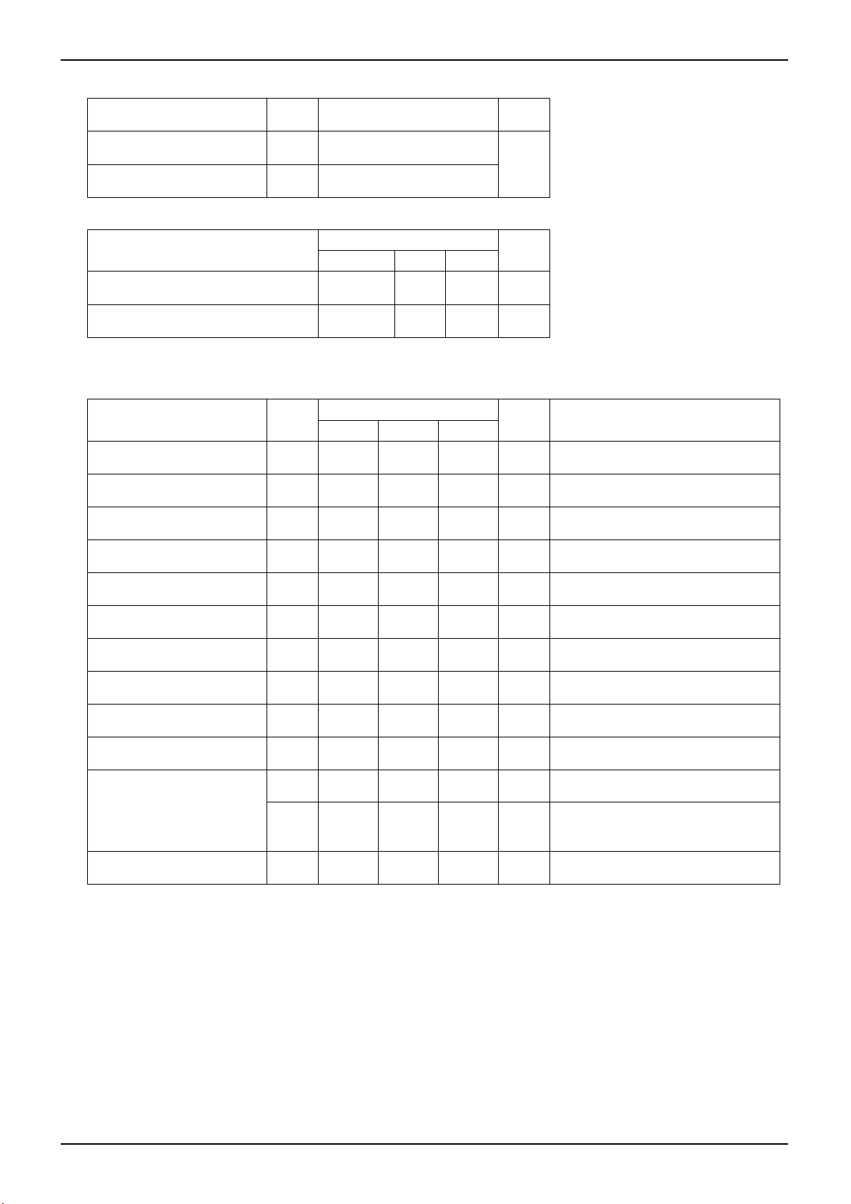
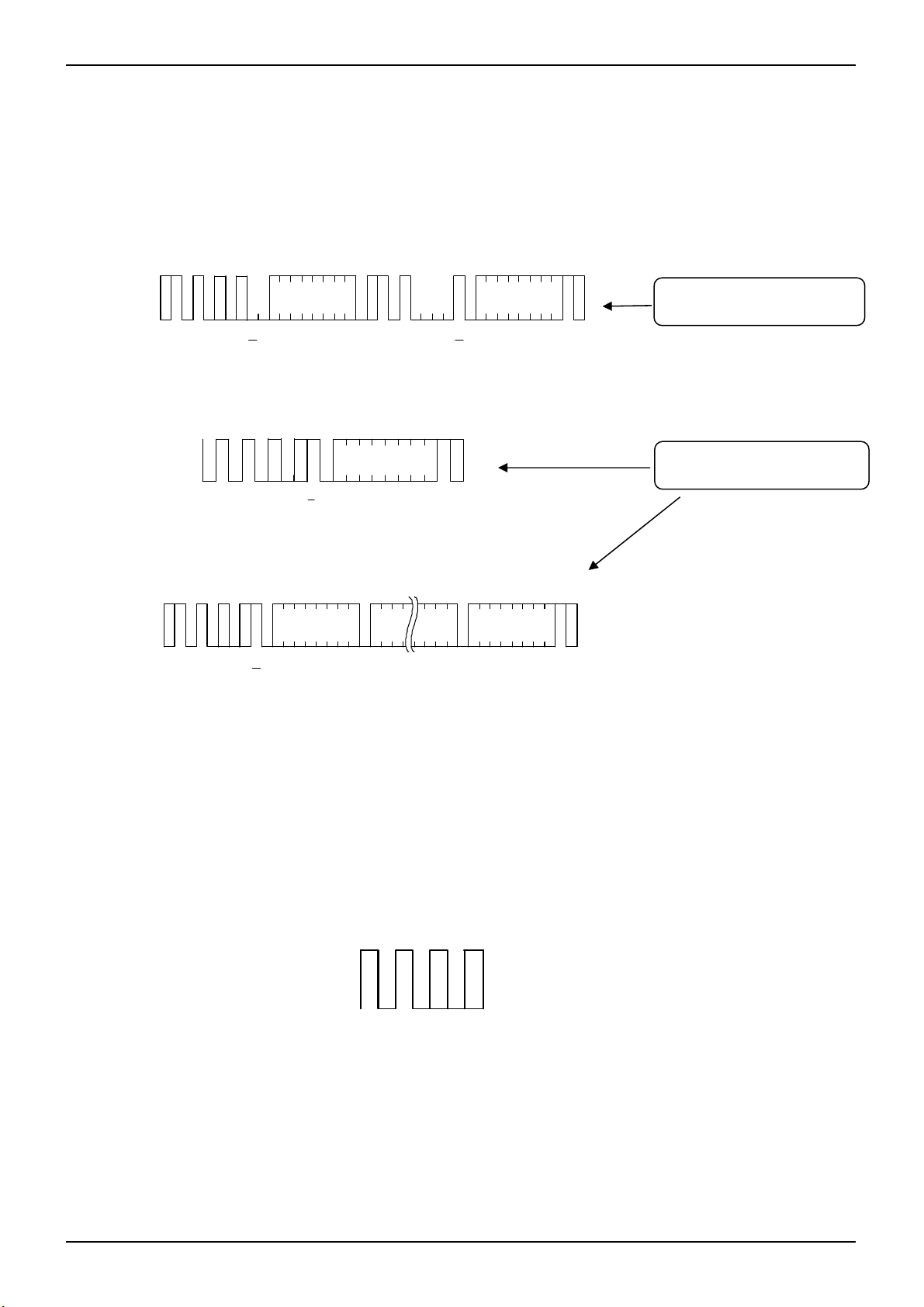
●Sync data input / output timing
SCL
SDA
(Input)
SDA
(Output)
tHD:STA tHD:DAT tSU:DAT
tBUF tPD tDH
○Input read at the rise edge of SCL
○Data output in sync with the fall of SCL
Fig.-1(a) Sync data input / output timing
SCL
tSU:ST
SDA
START BIT
Fig.1-(b) Start – stop bit timing
SCL
SDA
D0 ACK
Write data
(n-th address)
Stop condition Start c ondition
tLOW
tHIGH tR tF
SCL
SDA
WP
DATA(1)
D1 D0ACK
tSU:WP
DATA(n)
stop condition
fig.1-(d) WP timing at write execution
SCL
DATA(1)
D1 D0
SDA
tSU :STO tHD:ST
STOP BIT
WP
CK
tHIGH:WP
DATA(n)
CK
Fig.1-(e) WP timing at write cancel
○At write execution, in the area from the DO taken clock rise of the first
DATA (1), to tWR, set WP=“LOW”
○By setting WP “HIGH” in the area, write can be cancelled.
When it is set WP=“HIGH” during tWR, write is forcibly ended, and data
of address under access is not guaranteed, therefore write it once again.
tWR
Fig.1-(c) Write cycle timing
tWR
tWR
tHD:
Unit
WP
www.rohm.com
© 2010 ROHM Co., Ltd. All rights reserved.
3/18
2010.10 - Rev.
A
BU9833GUL-W
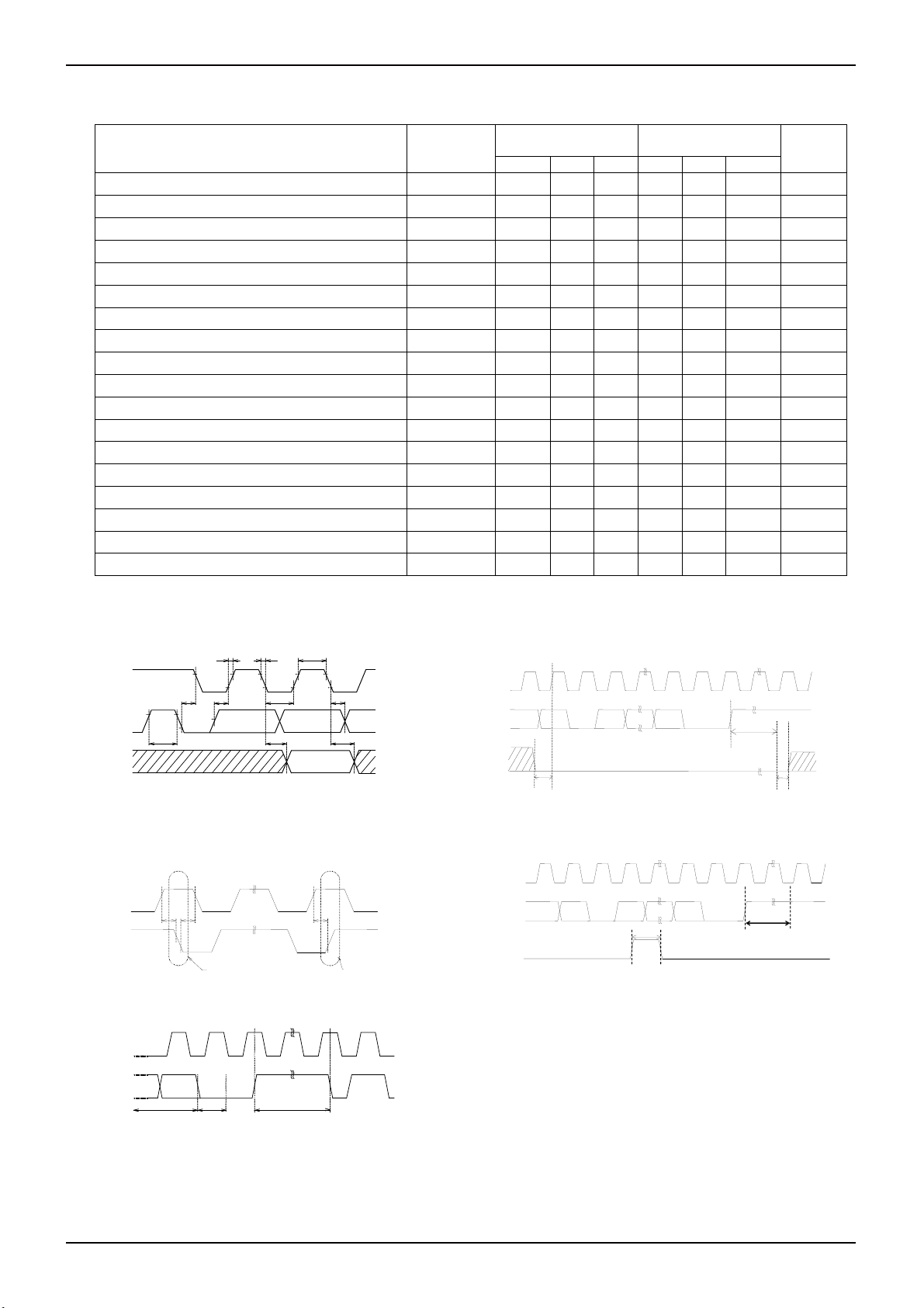
●Block diagram
VCC
GND
A2
●Pin assignment and description
Land No. Terminal name Input/ Output Function
2Kbit EE PROM array
9bit
Addr ess
decoder
Control circuit
High vol tage
generating circuti
Slav e – word
9bit
address register
START STOP
Power source
voltage detection
Fig.2 Block diagram
C
B
A
C1
○○
B1 B2
○○
A1
○○
C2
A2
12
Fig.3 BU9833GUL-W (bottom view)
ACK
8bit
Data
register
INDEX POST
Technical Note
WP
SCL
SDA
C2 VCC
-
Power Supply
C1 A2 IN Slave Address Set
B2 WP IN Write Protect Input
B1 GND
-
Ground (0V)
A2 SCL IN Serial Clock Input
A1 SDA IN/OUT
Slave and Word Address,
Serial Data Input, Serial Data Output *1
*1 An open drain output requires a pull-up resister.
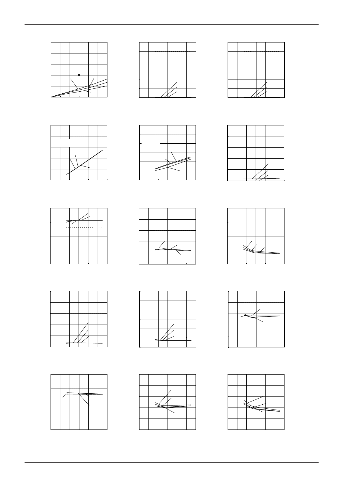
●Characteristic data (The following values are Typ. ones.)
6
5
4
3
VIH1,2,3[V]
2
1
0
0123456
SPEC
Ta= 85 ℃
Ta= -4 0℃
Ta= 25 ℃
Vcc[V]
Fig.4 H input voltage VIH1,2,3
(A2,SCL,SDA,WP)
6
5
4
Ta= 85 ℃
3
VIL1,2,3[V]
Ta= -4 0℃
2
Ta= 25 ℃
1
0
0123456
Fig.5 L input voltage VIL1,2,3
(A2,SCL,SDA,WP)
Vcc[V]
SPEC
1
0.8
0.6
VOL2[V]
0.4
SPEC
0.2
0
0123456
Ta= 85 ℃
Ta= 25 ℃
Ta= -4 0℃
IOL2[mA]
Fig.6 L output voltage VOL2-IOL2
CC=1.7V)
(V
www.rohm.com
© 2010 ROHM Co., Ltd. All rights reserved.
4/18
2010.10 - Rev.
A
BU9833GUL-W
Technical Note
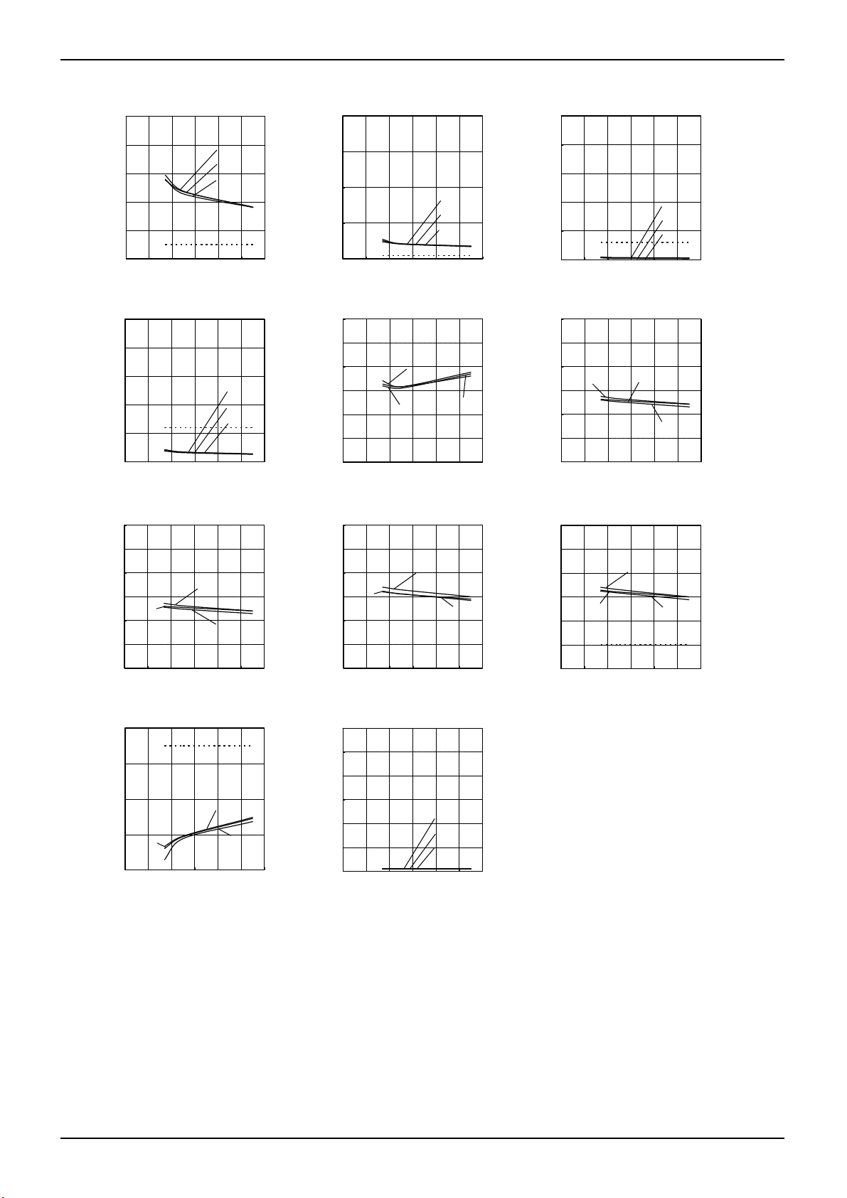
●Characteristic data
1
0.8
0.6
VOL1[V]
0.4
Ta= 85 ℃
0.2
0
0123456
Fig.7 L input voltage
VOL1-IOL1 (Vcc=2.5V)
2.5
2
fSCL=400kHz
DATA=AAh
1.5
ICC1[mA]
1
Ta= 25 ℃
Ta= 85 ℃
0.5
0
0123456
Fig.10 Consumption current
at write action Icc1 (f
10000
1000
fSCL[kHz]
Ta= 85 ℃
100
10
1
0123456
1
0.8
0.6
SPEC
0.4
tHD:STA[μs]
0.2
0
0123456
Fig.16 Start condition
hold time tHD:STA
200
100
0
tSU:DAT(HIGH)[ns]
-100
-200
0123456
SPEC
Ta= 85 ℃
Fig.19 Input data
setup time tSU:DAT
SPEC
IOL1[mA]
SPEC
Vcc[V]
SPEC
Vcc[V]
Vcc[V]
Vcc[V]
Ta= 25 ℃
Ta= -4 0℃
Ta= -4 0℃
SCL=400kHz)
Ta= -4 0℃
Ta= 25 ℃
SCL
Ta= 85 ℃
Ta= 25 ℃
Ta= -4 0℃
Ta= -4 0℃
Ta= 25 ℃
1.2
1
0.8
0.6
ILI[μA]
0.4
0.2
0
0123456
SPEC
Vcc[V]
Ta= 85 ℃
Ta= 25 ℃
Ta= -4 0℃
Fig.8 Input leak current
ILI (A2,SCL, WP)
0.6
fSCL=400kHz
DATA=AAh
SPEC
Ta= 25 ℃
Ta= 85 ℃
Vcc[V]
0.5
0.4
0.3
ICC2[mA]
0.2
0.1
0
0123456
Fig.11 Consumption current
at write action Icc2 (f
1
0.8
0.6
0.4
tHIGH [μs]
0.2
0
0123456
1
0.8
0.6
0.4
0.2
tHD:DAT(HIGH)[ns ]
0
-0.2
0123456
SCL=400kHz)
SPEC
Ta= 85 ℃
Ta= 25 ℃
Ta= -4 0℃
Vcc[V]
SPEC
Ta= 85 ℃
Ta= 25 ℃
Ta= -4 0℃
Vcc[V]
Fig.17 Start condition
setup time tSU:STA
1
0.8
0.6
0.4
tPD0 [μs]
0.2
0
SPEC
Ta= 85 ℃
Ta= 25 ℃
Ta= -4 0℃
SPEC
0123456
Vcc[V]
Fig.20 Output data delay time
tPD0
Ta= -4 0℃
1.2
1
0.8
0.6
ILO[μA]
0.4
0.2
0
SPEC
Ta= 85 ℃
Ta= 25 ℃
Ta= -4 0℃
0123456
Vcc[V]
Fig.9 Output leak current
ILO (SDA)
2.5
2
1.5
ISB[μA]
1
0.5
0
0123456
SPEC
Ta= 85 ℃
Ta= 25 ℃
Ta= -4 0℃
Vcc[V]
Fig.12 Standby current I
1.6
1.2
0.8
tLOW[μs]
0.4
0
0123456
SPEC
Ta= 85 ℃
Ta= 25 ℃
Vcc[V]
Ta= -4 0℃
Fig.15 Data clock “L” time tLOWFig.14 Data clock “H” time tHIGHFig.13 SCL frequency f
50
0
-50
-100
tHD:DAT(HIGH)[ns ]
-150
-200
SPEC
Ta= 85 ℃
Ta= 25 ℃
Ta= -4 0℃
0123456
Vcc[V]
Fig.18 Input data
hold time tHD:DAT
1
0.8
0.6
0.4
tPD1 [μs]
0.2
0
0123456
SPEC
Ta= 85 ℃
Ta= 25 ℃
Ta= -4 0℃
SPEC
Vcc[V]
Fig.21 Output data delay time
tPD1
SB
www.rohm.com
© 2010 ROHM Co., Ltd. All rights reserved.
5/18
2010.10 - Rev.
A
BU9833GUL-W
●Characteristic data
1
0.8
0.6
tDH0[μs]
0.4
0.2
0
SPEC
0123456
Fig.22 Output data hold time
5
4
3
tBUF[μs]
2
1
SPEC
0
0123456
Fig.25 Bus release time
before transfer start tBUF
0.6
0.5
0.4
0.3
Ta= 25 ℃
tI(SCL L) [μ s]
0.2
0.1
0
0123456
SPEC
Fig.28 Noise removal time
tI (SCL L)
0.2
0
SPEC
-0.2
tSU:WP[μs]
-0.4
Ta= 25 ℃
-0.6
0123456
Fig.31 WP setup time
tSU:WP
Vcc[V]
tDH1
Vcc[V]
Ta= -4 0℃
Vcc[V]
Vcc[V]
Ta= 85 ℃
Ta= 25 ℃
Ta= -4 0℃
Ta= -4 0℃
Ta= 25 ℃
Ta= 85 ℃
Ta= 85 ℃
Ta= 85 ℃
Ta= -4 0℃
4
3
2
tDH1[μs]
1
SPEC
0
0123456
Ta= 85 ℃
Ta= 25 ℃
Ta= -4 0℃
Vcc[V]
Fig.23 Output data hold time
SPEC
tDH1
Ta= -4 0℃
Ta= 85 ℃
Vcc[V]
Ta= 25 ℃
6
5
4
3
tWR[ms]
2
1
0
0123456
Fig.26 Internal write cycle time
tWR
0.6
0.5
0.4
Ta= 25 ℃
0.3
0.2
tI(SDA H) [μ s]
0.1
0
0123456
Fig.29 Noise removal time
Ta= -4 0℃
Ta= 85 ℃
SPEC
Vcc[V]
tI (SDA H)
1.2
1
0.8
0.6
tHIGH:WP[μs]
0.4
0.2
0
SPEC
Ta= -4 0℃
Ta= 25 ℃
Ta= 85 ℃
0123456
Vcc[V]
Fig.32 WP valid time
tHIGH: WP
Technical Note
5
4
3
2
tSU:STO[μs]
1
0
Fig.24 Stop condition setup time
SPEC
0123456
Vcc[V]
tSU:STO
0.6
0.5
0.4
Ta= -4 0℃
0.3
tI(SCL H) [μ s]
0.2
0.1
0
SPEC
0123456
Fig.27 Noise removal time
Vcc[V]
tI (SCL H)
0.6
0.5
0.4
0.3
Ta= 25 ℃
tI(SDA L) [μ s]
0.2
0.1
0
Fig.30 Noise removal time
SPEC
0123456
Vcc[V]
tI (SDA L)
Ta= 85 ℃
Ta= 25 ℃
Ta= -4 0℃
Ta= 25 ℃
Ta= 85 ℃
Ta= -4 0℃
Ta= 85 ℃
www.rohm.com
© 2010 ROHM Co., Ltd. All rights reserved.
6/18
2010.10 - Rev.

A
BU9833GUL-W
r
ACK
A
A
A
Technical Note
●I2C BUS communication
○I2C BUS data communication
2
C BUS data communication starts by start condition input, and ends by stop condition input. Data is always 8bit long,
I
and acknowledge is always required after each byte.
I2C BUS carries out data transmission with plural devices connected by 2 communication lines of serial data (SDA) and
serial clock (SCL).
Among devices, there are “master” that generates clock and control communication start and end, and “slave” that is
controlled by addresses peculiar to devices.
EEPROM becomes “slave”. And the device that outputs data to bys during data communication is called “transmitter”,
and the device that receives data is called “receiver “.
SDA
SCL
condition condition
1-7 1-7
89 89 89
S P
DDRESS START R/W ACK
1-7
CKDAT
DATA
STOP
Fig.33 Data transfer timing
○Start condition (start bit recognition)
・ Before executing each command, start condition (start bit) where SDA goes from “HIGH” down to “LOW”
when SCL is “HIGH” is necessary.
・This IC always detects whether SDA and SCL are in start condition (start bit) of not, therefore, unless this condition is
satisfied, any command is executed.
○Stop condition (stop bit recognition)
・ Each command can be ended by SDA rising from “LOW” to “HIGH” when stop condition (stop bit), namely,
SCL is “HIGH”.
○Acknowledge (ACK) signal
・This acknowledge (ACK) signal is a software rule to show whether data transfer has been made normally or not. In
master and slave, the device (μ-COM at slave address input of write command, read command, and this IC at data
output of read command) at the transmitter (sending) side releases the bus after output of 8bit data.
・This device (this IC at slave address input of write command , read command , and μ-COM at data output of read
command) at the receiver (receiving) side sets SDA “LOW” during 9 clock cycles, and outputs acknowledge signal
(ACK signal) showing that it has received the 8bit data.
・This IC, after recognizing start condition and slave address (8bit), outputs acknowledge signal (ACK signal) “LOW”.
・Each write action outputs acknowledge signal (ACK signal) “LOW”, at receiving 8bit data (word address and write data).
・Each read action outputs 8bit data (read data), and detects acknowledge signal (ACK signal) “LOW”.
・When acknowledge signal (ACK signal) is detected, and stop condition is not sent from the master (μ-COM) side,
this IC continues data output. When acknowledge signal (ACK signal) is not detected, this IC stops data transfer,
and recognizes stop condition (stop bit), and ends read action.
And this IC gets in standby status.
○Device addressing
・Output slave address after start condition from master.
・The significant 4 bits of slave address are used for recognizing a device type.
The device code of this IC is fixed to “1010”.
・Next slave addressed (A2 --- device address) are for selecting devices, and plural ones can be used on a same bus
according to the number of device addresses.
・The most insignificant bit (
W/R --- WRITE/READ ) of slave address is used for designating write or read action, and is
as shown below.
Setting W/R to 0 --- write (setting 0 to word address setting of random read)
Setting
W/R
to 1 --- read
Type Slave address
Maximum numbe
of connected buses
BU9833GUL-W
PS is page select bits.
www.rohm.com
© 2010 ROHM Co., Ltd. All rights reserved.
1 0 1 0 A2 0 0 W/R
7/18
2
2010.10 - Rev.
A
BU9833GUL-W
A
A
S
A
A
A
A
A
DATA(n)
DATA(n+15)
WA
Technical Note
●Command
○Write cycle
・Arbitrary data is written to EEPROM. When to write only 1 byte, byte write is normally used, and when to write
continuous data of 2 bytes or more, simultaneous write is possible by page write cycle.
SD
LINE
WP
S
T
A
SLAVE
R
ADDRESS
T
A2
W
R
I
T
E
0
0
R
C
/
K
W
WORD
ADDRESS
W
7
W
0
C
K
DAT
D7 1 1 0 0
D0
T
O
P
C
K
Fig.34 Byte write cycle
SDA
LINE
S
T
A
R
T
ADDRESS
10 010 0 A2
SLAVE
P
W
R
I
W
T
E
R
/
WORD
ADDRESS (n)
WA
7 D0 D7 D0
A
C
K
0
A
C
K
A
C
K
S
T
O
P
A
C
K
Fig.35 Page write cycle
・Data is written to the address designated by word address (n-th address).
・By issuing stop bit after 8bit data input, write to memory cell inside starts.
・When internal write is started, command is not accepted for tWR (5ms at maximum).
・By page write cycle, the following can be written in bulk. Up to 16 bytes
And when data of the maximum bytes or higher is sent, data from the first byte is overwritten.
(Refer to “Internal address increment” of “Notes on page write cycle” in P8/16.)
・As for page write cycle of BU9833GUL-W, after page select bit (PS) of slave address is designated arbitrarily, by
continuing data input of 2 bytes or more, the address of insignificant 4 bits is incremented internally, and data up to 16
bytes can be written.
Note)
1
00
10
A2
0
Fig.36 Difference of slave address of each type
www.rohm.com
© 2010 ROHM Co., Ltd. All rights reserved.
8/18
2010.10 - Rev.

A
BU9833GUL-W
A
A
)
A
A
○Notes on write cycle continuous input
SDA
LINE
S
T
A
SL AVE
R
ADDRESS
T
10 0 10 0 A2
W
R
I
T
E
WA
7
R
C
/
K
W
Note)
1
Fig.38 Difference of each type of slave address
○Notes on page write cycle
List of numbers of page write
Number of Pages 16Byte
Product number BU9833GUL-W
The above numbers are maximum bytes
for respective types.
Any types below these can be written.
1page = 16 bytes, but the page write cycle write time is 5ms
at maximum for 16byte bulk write.
It does not stand 5ms at maximum x 16 bytes = 80ms (Max.).
WORD
ADDRES S(n)
WA
DA TA( n)
0
C
K
Fig.37 Page write cycle
0
0 0
1
A2
0
DATA(n+15
D0 D7 D0
C
K
At ST OP (sto p bit),
Wr ite s tarts .
S
T
O
P
C
K
tWR (maximum : 5ms)
Co mm and is no t ac cept ed fo r th is peri od.
○Internal address increment
Page write mode
WA7 ----- WA4 WA3 WA2 WA1 WA0
0 ----- 0 0 0 0 0
0 ----- 0 0 0 0 0
0 ----- 0 0 0 0 0
0Eh
---------
0 ----- 0 1 1 1 0
0 ----- 0 1 1 1 1
0 ----- 0 0 0 0 0
S
T
A
R
T
1 100
Next command
Technical Note
---------
Increment
○Write protect terminal (WP)
・Write protect function
When WP terminal is set Vcc (H level), data rewrite of all addresses is prohibited. When it is set GND (L level), data
rewrite of all addresses is enabled. Be sure to connect this terminal to Vcc or GND, or control it to H level or L level.
Do not use it open.
At extremely low voltage at power ON/OFF, by setting the WP terminal “H”, mistake write can be prevented.
During tWR, set the WP terminal always to “L”. If it is set “H”, write is forcibly terminated.
Significant bit is fixed.
No digit up
For example, when it is started from address 0Eh, therefore, increment is made
as below,
0Eh→0Fh→00h→01h ---, which please note.
*0Eh --- 0E in hexadecimal, therefore, 00001110 becomes a binary number.
www.rohm.com
© 2010 ROHM Co., Ltd. All rights reserved.
9/18
2010.10 - Rev.
A
BU9833GUL-W
S
)
S
S
A
A
(n)
)
Technical Note
●Command
○Read cycle
Data of EEPROM is read. In read cycle, there are random read cycle and current read cycle.
Random read cycle is a command to read data by designating address, and is used generally.
Current read cycle is a command to read data of internal address register without designating address, and is used when
to verify just after write cycle. In both the read cycles, sequential read cycle is available, and the next address data next
address data can be read in succession.
SDA
LINE
T
A
R
T
10 0
SLAVE
ADDRESS
10 0 A2
W
R
I
T
E
R
/
W
WA
A
C
K
ADDRESS(n)
7
WORD
WA
0
T
A
R
T
A
C
K
SLAV E
ADDRESS
10 010 A2
R
E
A
DATA(n
D
0
D0
D7
A
R
C
/
K
W
S
T
O
P
It is necessary to input “H”
to the last ACK.
A
C
K
Fig.39 Random Read cycle
SDA
LINE
S
T
A
LAVE
R
ADDRESS
T
R
E
A
D
0 A2 D7 1 1 0 0
0 D0
R
/
C
W
K
DATA
S
T
O
P
It is necessary to input “H”
to the last ACK.
C
K
Fig.40 Current read cycle
SDA
LINE
S
T
A
R
T
10 0
SLAVE
ADDRESS
A2
10 0
R
E
A
D
A
R
C
/
K
W
DATA
D0 D7 D0 D7
A
C
K
DA TA(n+x
A
C
K
S
T
O
P
A
C
K
Fig.41 Sequential read cycle
・In random read cycle, data of designated word address can be read.
・When the command just before current read cycle is random read cycle, current read cycle (each including sequential
read cycle), data of incremented last read address (n-th) address, i.e., data of the (n+1)-th address is output.
・When ACK signal “LOW” after D0 is detected, and stop condition is not sent from the master (μ-COM) side, the next
address data can be read in succession.
・Read cycle is ended by stop condition where “H” is input to ACK signal after D0 and SDA signal is started at SCL
signal “H”.
・When “H” is not input to ACK signal after D0, sequential read gets in, and the next data is output.
Therefore, read command cycle cannot be ended. When to end read command cycle, be sure input stop condition to
input “H” to ACK signal after D0, and to start SDA at SCL signal “H”.
・Sequential read is ended by stop condition where “H” is input to ACK signal after arbitrary D0 and SDA is started at SCL
signal “H”.
Note)
1
0 0
1
A2
0
0
Fig.42 Difference of slave address of each type
www.rohm.com
© 2010 ROHM Co., Ltd. All rights reserved.
10/18
2010.10 - Rev.

A
BU9833GUL-W
A
A
A
A
A
A
Technical Note
●Software reset
Software reset is executed when to avoid malfunction after power on, and to reset during command input. Software reset
has several kinds, and 3 kinds of them are shown in the figure below. (Refer to Fig.43(a), Fig.43(b) and Fig.43(c).) In
dummy clock input area, release the SDA bus (“H” by pull up). In dummy clock area, ACK output and read data “0” (both “L”
level) may be output from EEPROM, therefore, if “H” is input forcibly, output may conflict and over current may flow, leading
to instantaneous power failure of system power source or influence upon devices.
SCL
SDA
Fig.43-(a) The case of dummy clock + START + START + command input
Dummy clock x14
2 13
1
14
Star t x2
Normal command
Normal command
SCL
SDA
Star t
Fig.43-(b) The case of START + 9 dummy clocks + START + command input
Dummy clock x9 Start
1
2
8
9
Normal command
Normal command
SCL
SDA
1
Fig.43-(c) START x 9 + command input
Star t x 9
3
2
7
8
9
Normal command
Normal command
* Start normal command from START input.
●Acknowledge polling
During internal write execution, all input commands are ignored, therefore ACK is not sent back. During internal automatic
write execution after write cycle input, next command (slave address) is sent, and if the first ACK signal sends back “L”,
then it means end of write action, while if it sends back “H”, it means now in writing. By use of acknowledge polling, next
command can be executed without waiting for tWR=5ms.
When to write continuously, W/R = 0, when to carry out current read cycle after write, slave address W/R = 1 is sent,
and if ACK signal sends back “L”, then execute word address input and data output and so forth.
First write command
…
S
T
A
R
T
Write command
S
T
Slave
A
address
R
T
tWR
S
S
T
O
P
C
K
H
S
T
A
R
T
Slave
T
A
address
R
T
Slave
address
C
K
H
Second write command
C
K
address
L
tWR
Word
During internal write,
ACK = HIGH is sent back.
S
Slave
T
A
address
R
T
C
Data
K
L
After completion of internal write,
ACK = LOW is sent back, so input
next word address and data in
succession.
…
C
K
H
S
T
C
O
K
P
L
Fig.44 Case to continuously write by acknowledge polling
www.rohm.com
© 2010 ROHM Co., Ltd. All rights reserved.
11/18
2010.10 - Rev.

A
BU9833GUL-W
Technical Note
●WP valid timing (write cancel)
WP is usually to “H” or “L”, but when WP is used to cancel write cycle and so forth, pay attention to the following WP valid timing.
During write cycle execution, in cancel valid area, by setting WP = “H”, write cycle can be cancelled. In both byte write cycle
and page write cycle, the area from the first start condition of command to the rise of clock to taken in D0 of data (in page
write cycle, the first byte data) is cancel invalid area.
WP input in this area becomes Don’t care. Set the setup time to rise of D0 taken SCL 100ns or more. The area from the rise
of SCL to take in D0 to the end of internal automatic write (tWR) is cancel valid area. And, when it is set WP = “H” during
tWR, write is ended forcibly, data of address under access is not guaranteed, therefore, write it once again. (Refer to Fig.45.)
After execution of forced end by WP, standby status gets in, so there is no need to wait for tWR (5ms at maximum).
SDA
WP
·Rise of D0 taken clock
SCL
SDA
Enlarged view
S
T
A
R
T
Slave
address
A
C
K
L
D0
D1
Word
address
WP cancel invalid area
ACK
A
C
D6
D7
K
L
D5
D4
D3
D2
A
C
D1 D0
K
L
WP cancel valid area
Data is not written
SCL
SDA
Data
·Rise of SDA
D0
ACK
Enlarged view
A
S
C
T
K
O
L
P
Write forced end
tWR
Data not
guaranteed
Fig. 45 WP valid timing
●Command cancel by start condition and stop condition
During command input, by continuously inputting start condition and stop condition, command can be cancelled. (Refer to fig.46)
However, in ACK output area and during data read, SDA bus may output “L”, and in this case, start condition and stop
condition cannot be input, so reset is not available. Therefore, execute software reset. and when command is cancelled by
start, stop condition, during random read cycle, sequential read cycle, or current read cycle, internal setting address is not
determined, therefore, it is not possible to carry out current read cycle in succession. When to carry out read cycle in
succession, carry out random read cycle.
SCL
SDA
1
0 0
1
Start condition
Stop condition
Fig. 46 Case of cancel by start, stop condition during slave address input
www.rohm.com
© 2010 ROHM Co., Ltd. All rights reserved.
12/18
2010.10 - Rev.
A
BU9833GUL-W
3
●I/O peripheral circuit
○Pull up resistance of SDA terminal
SDA is NMOS open drain, so requires pull up resistance. As for this resistance value (R
this resistance value from microcontroller V
limited. The smaller the R
, the larger the consumption current at action.
PU
, IL, and VOL-IOL characteristics of this IC. If RPU is large, action frequency is
IL
○Maximum value of RPU
The maximum value of R
is determined by the following factors.
PU
(1) SDA rise time to be determined by the capacity (CBUS) of bus line of R
And AC timing should be satisfied even when SDA rise time is late.
A
(2) The bus electric potential ○
SDA bus and R
should sufficiently secure the input “H” level (VIH) of microcontroller and EEPROM including
PU
to be determined by input leak total (IL) of device connected to bus at output of “H” to
recommended noise margin 0.2Vcc.
V
CC-ILRPU
-0.2 VCC ≥ VIH
0.8V
∴ RPU ≦
CC-VIH
IL
Microcontroller
Ex.) When VCC =3V, IL=10μA, VIH=0.7 Vcc
from (2)
R
PU
≦
0.8×3-0.7×3
-6
10×10
Technical Note
), select an appropriate value to
PU
and SDA should be tR or below.
PU
BU9833GUL-W
PU
R
SDA terminal
IL
IL
A
Bus line
capacity CBUS
≦
Fig.47 I/O circuit diagram
[kΩ]
300
○Minimum value of RPU
The minimum value of R
is determined by the following factors.
PU
(1) When IC outputs LOW, it should be satisfied that VOLMAX = 0.4V and IOLMAX = 3mA.
VCC-VOL
RPU IOL
≦
IOL
∴
RPU
≧
CC-VOL
V
(2) VOLMAX = 0.4V should secure the input “L” level (VIL) of microcontroller and EEPROM including recommended
noise margin 0.1VCC.
≤ VIL – 0.1V
V
OLMAX
CC
Ex.) When V
From (1),
And
= 3V, V
CC
= 0.4V, IOL = 3mA, microcontroller, EEPROM VIL = 0.3VCC
OL
3-0.4
≥
∴R
PU
3 x 10
-
≥867[Ω]
= 0.4[V]
V
OL
V
= 0.3 x 3
IL
=0.9 [V]
Therefore, the condition (2) is satisfied.
○Pull up resistance of SCL terminal
When SCL control is made at CMOS output port, there is no need, but in the case there is timing where SCL becomes
“Hi-Z”, add a pull up resistance. As for the pull up resistance, one of several kΩ ~ several ten kΩ is recommended in
consideration of drive performance of output port of microcontroller.
●A2, WP process
○Process of device address terminals (A2)
Check whether the set device address coincides with device address input sent from the master side or not, and select
one among plural devices connected to a same bus. Connect this terminal to pull up of pull down, or V
or GND.
CC
○Process of WP terminal
WP terminal is the terminal that prohibits and permits write in hardware manner. In “H” status, only READ is available and
WRITE of all addresses is prohibited. In the case of “L”, both are available. In the case to use it as an ROM, it is
recommended to connect it to pull up or V
. In the case to use both READ and WRITE, control WP terminal or connect it
CC
to pull down or GND.
www.rohm.com
© 2010 ROHM Co., Ltd. All rights reserved.
13/18
2010.10 - Rev.

A
BU9833GUL-W
A
A
Technical Note
●Cautions on microcontroller connection
○Rs
2
C BUS, it is recommended that SDA port is of open drain input / output. However, when to use COMS input / output
In I
of tri state to SDA port, insert a series resistance Rs between the pull up resistance R
and the SDA terminal of
PU
EEPROM. This controls over protection of SDA terminal against surge. Therefore, even when SDA port is open drain
input / output, Rs can be used.
RPU
S
R
SCL
SDA
“H” output of
microcontroller
CK
“L” output of EEPROM
Microcontroller
EEPROM
Fig.48 I/O circuit diagram
Over current flows to SDA line by “H” output of
microcontroller and “L” output of EEPROM.
Fig.49 Input / output collision timing
○Maximum value of Rs
The maximum value of Rs is determined by the following relations.
(1) SDA rise time to be determined by the capacity (CBUS) of bus line of R
and SDA should be tR or below.
PU
And AC timing should be satisfied even when SDA rise time is late.
(2) The bus electric potential A to be determined by RPU and Rs at the moment when EEPROM outputs “L” to SDA bus
should sufficiently secure the input “L” level (V
) of microcontroller including recommended noise margin 0.1VCC.
IL
VCC
RPU
S
R
IOL
Bus line
capacity CBUS
VOL
Example) When VCC=3V, VIL=0.3VCC, VOL=0.4V, RPU=20kΩ,
(VCC-VOL)×RS
RPU+RS
∴ RS ≦
+ VOL+0.1VCC≦ VIL
VIL-VOL-0.1VCC
1.1VCC-VIL
× RPU
VIL
Microcontroller
Fig.50 I/O circuit diagram
EEPROM
From (2) RS ≦
≦ 1.67[kΩ]
0.3×3-0.4-0.1×3
1.1×3-0.3×3
×20×103
○Minimum value of Rs
The minimum value of Rs is determined by over current at bus collision. When over current flows, noises in power source
line, and instantaneous power failure of power source may occur. When allowable over current is defined as I, the
following relation must be satisfied. Determine the allowable current in consideration of impedance of power source line
in set and so forth. Set the over current to EEPROM 10mA or below.
VCC
RS
≦ I
R
PU
R
"L" output
S
RS
≧
VCC
I
Over current I
"H" output
Microcontroller
www.rohm.com
© 2010 ROHM Co., Ltd. All rights reserved.
Fig.51 I/O Circuit diagram
EEPROM
14/18
Example) When Vcc =3V, I = 10mA,
RS ≧
3
10×10-3
≧ 300[Ω]
2010.10 - Rev.
A
BU9833GUL-W
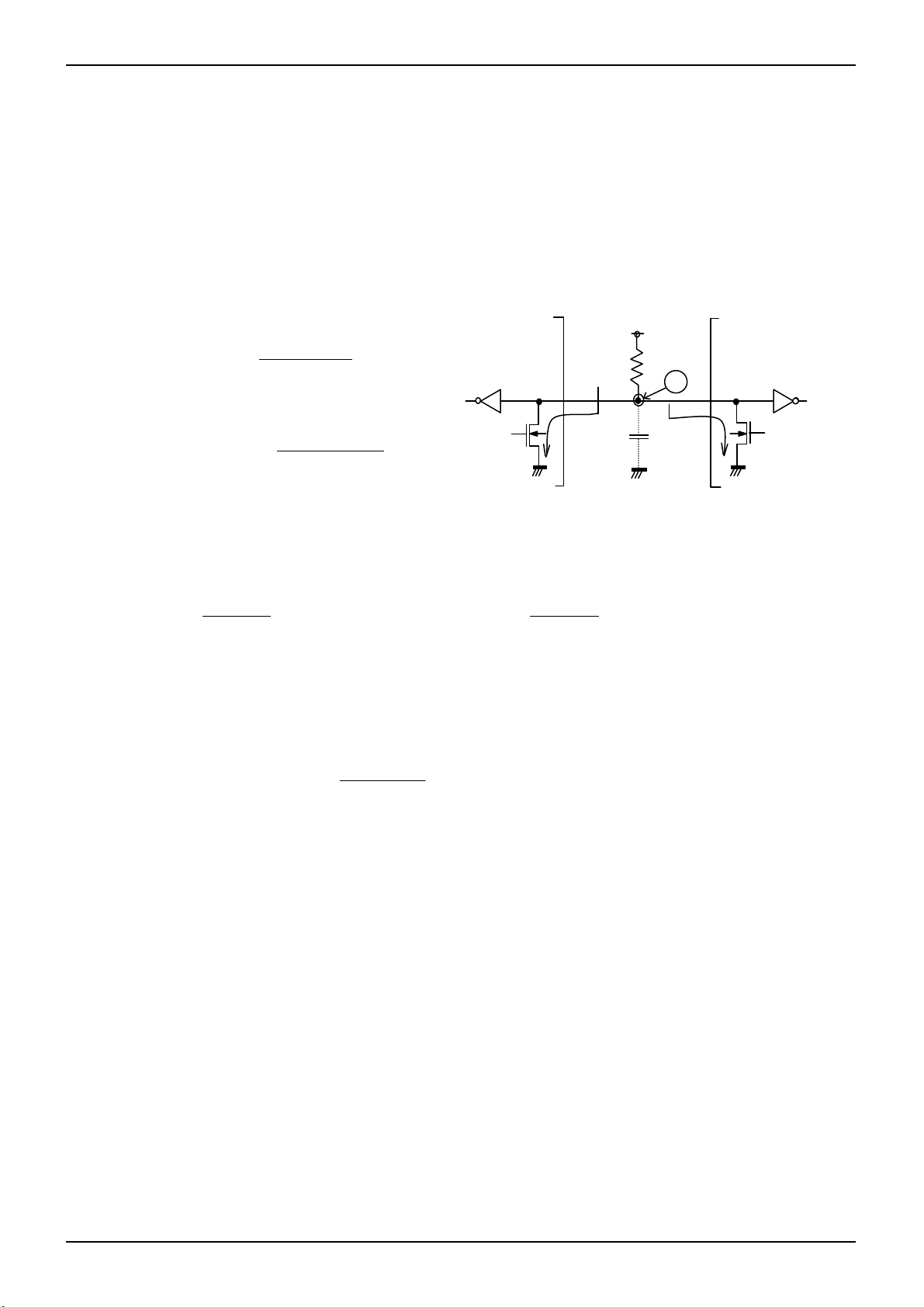
●I2C BUS input / output circuit
○Input (A2,SCL)
○Input / output (SDA)
○Input (WP)
Technical Note
Fig.52 Input pin circuit diagram
Fig.53 Input / output pin circuit diagram
Fig.54 Input pin circuit diagram
www.rohm.com
© 2010 ROHM Co., Ltd. All rights reserved.
15/18
2010.10 - Rev.

A
BU9833GUL-W
A
A
Technical Note
●Notes on power ON
At power on, in IC internal circuit and set, Vcc rises through unstable low voltage area, and IC inside is not completely reset,
and malfunction may occur. To prevent this, function of POR circuit and LVCC circuit are equipped. To assure the action,
observe the following conditions at power on.
1. Set SDA= “H” and SCL = “L” or “H”.
2. Start power source so as to satisfy the recommended conditions of tR, tOFF, and Vbot for operating POR circuit.
VCC
tOFF
0
Fig. 55 Rise waveform diagram
tR
Vbot
, t
Recommended conditions of t
t
t
R
, Vbot
R
OFF
Vbot
OFF
10ms or below 10ms or higher 0.3V or below
100ms or below 10ms or higher 0.2V or below
3. Set SDA and SCL so as not to become “Hi-Z”.
When the above conditions 1 and 2 cannot be observed, take the following countermeasures.
a) In the case when the above condition 1 cannot be observed. When SDA becomes “L” at power on.
→ Control SCL and SDA as shown below, to make SCL and, “H” and “H”.
VCC
SCL
tLOW
SDA
fter Vcc becomes stable
Fig.56 When SCL =”H” and SDA = “L”
tSU:DAT tDH
fter Vcc becomes stable
tSU:DAT
Fig.57 When SCL = “H” and SDA = “L”
b) In the case when the above condition 2 cannot be observed.
→ After power source becomes stable, execute software reset (P10).
c) In the case when the above conditions 1 and 2 cannot be observed.
→ Carry out a), and then carry out b).
●Low voltage malfunction prevention function
LVCC circuit prevents data rewrite action at low power, and prevents wrong write. At LVCC voltage (Typ. = 1.2V) or below, it
prevent data rewrite.
●Vcc noise countermeasures
○Bypass capacitor
When noise or surge gets in the power source line, malfunction may occur, therefore, for removing tese, it is
recommended to attach a by pass capacitor (0.1μF) between IC Vcc and GND. At that moment , attach it as close to IC
as possible.
And, it is also recommended to attach a bypass capacitor between board Vcc and GND.
www.rohm.com
© 2010 ROHM Co., Ltd. All rights reserved.
16/18
2010.10 - Rev.

A
BU9833GUL-W
●Notes for use
(1) Described numeric values and data are design representative values, and the values are not guaranteed.
(2) We believe that application circuit examples are recommendable, however, in actual use, confirm characteristics further
sufficiently. In the case of use by changing the fixed number of external parts, make your decision with sufficient margin in
consideration of static characteristics and transition characteristics and fluctuations of external parts and our LSI.
(3) Absolute maximum ratings
If the absolute maximum ratings such as impressed voltage and action temperature range and so forth are exceeded, LSI
may be destructed. Do not impress voltage and temperature exceeding the absolute maximum ratings. In the case of fear
exceeding the absolute maximum ratings, take physical safety countermeasures such as fuses, and see to it that
conditions exceeding the absolute maximum ratings should not be impressed to LSI.
(4) GND electric potential
Set the voltage of GND terminal lowest at any action condition. Make sure that each terminal voltage is lower than that of
GND terminal.
(5) Thermal design
In considereation of permissible loss in actual use condition, carry out heat design with sufficient margin.
(6) Terminal to terminal shortcircuit and wrong packaging
When to package LSI onto a board, pay sufficient attention to LSI direction and displacement. Wrong packaging may
destruct LSI. And in the case of shortcircuit between LSI terminals and terminals and power source, terminal and GND
owing to foreign matter, LSI may be destructed.
(7) Use in a strong electromagnetic field may cause malfunction, therefore, evaluate design sufficiently.
Technical Note
www.rohm.com
© 2010 ROHM Co., Ltd. All rights reserved.
17/18
2010.10 - Rev.

A
BU9833GUL-W
●Ordering part number
B U 9 8 3 3 G U L - W E 2
Technical Note
Part No. Part No. Package
VCSP50L1
(BU9833GUL-W)
1PIN MARK
6-φ0.25±0.05
0.05
BA
(φ0.15)INDEX POST
C
B
A
0.385±0.1
1.27±0.1
1
2
0.5
0.08 S
A
B
1.50±0.1
0.55MAX
0.10±0.05
S
0.25±0.1
P=0.5×2
(Unit : mm)
GUL : VCSP50L1
<Tape and Reel information>
Embossed carrier tapeTape
Quantity
Direction
of feed
3000pcs
E2
The direction is the 1pin of product is at the upper left when you hold
()
reel on the left hand and you pull out the tape on the right hand
Reel
W-CELL Packaging and forming specification
E2: Embossed tape and reel
1pin
Order quantity needs to be multiple of the minimum quantity.
∗
Direction of feed
www.rohm.com
© 2010 ROHM Co., Ltd. All rights reserved.
18/18
2010.10 - Rev.

Notes
No copying or reproduction of this document, in part or in whole, is permitted without the
consent of ROHM Co.,Ltd.
The content specied herein is subject to change for improvement without notice.
The content specied herein is for the purpose of introducing ROHM's products (hereinafter
"Products"). If you wish to use any such Product, please be sure to refer to the specications,
which can be obtained from ROHM upon request.
Examples of application circuits, circuit constants and any other information contained herein
illustrate the standard usage and operations of the Products. The peripheral conditions must
be taken into account when designing circuits for mass production.
Great care was taken in ensuring the accuracy of the information specied in this document.
However, should you incur any damage arising from any inaccuracy or misprint of such
information, ROHM shall bear no responsibility for such damage.
The technical information specied herein is intended only to show the typical functions of and
examples of application circuits for the Products. ROHM does not grant you, explicitly or
implicitly, any license to use or exercise intellectual property or other rights held by ROHM and
other parties. ROHM shall bear no responsibility whatsoever for any dispute arising from the
use of such technical information.
Notice
The Products specied in this document are intended to be used with general-use electronic
equipment or devices (such as audio visual equipment, ofce-automation equipment, communication devices, electronic appliances and amusement devices).
The Products specied in this document are not designed to be radiation tolerant.
While ROHM always makes efforts to enhance the quality and reliability of its Products, a
Product may fail or malfunction for a variety of reasons.
Please be sure to implement in your equipment using the Products safety measures to guard
against the possibility of physical injury, re or any other damage caused in the event of the
failure of any Product, such as derating, redundancy, re control and fail-safe designs. ROHM
shall bear no responsibility whatsoever for your use of any Product outside of the prescribed
scope or not in accordance with the instruction manual.
The Products are not designed or manufactured to be used with any equipment, device or
system which requires an extremely high level of reliability the failure or malfunction of which
may result in a direct threat to human life or create a risk of human injur y (such as a medical
instrument, transportation equipment, aerospace machinery, nuclear-reactor controller, fuelcontroller or other safety device). ROHM shall bear no responsibility in any way for use of any
of the Products for the above special purposes. If a Product is intended to be used for any
such special purpose, please contact a ROHM sales representative before purchasing.
If you intend to export or ship overseas any Product or technology specied herein that may
be controlled under the Foreign Exchange and the Foreign Trade Law, you will be required to
obtain a license or permit under the Law.
Thank you for your accessing to ROHM product informations.
More detail product informations and catalogs are available, please contact us.
ROHM Customer Support System
www.rohm.com
© 2010 ROHM Co., Ltd. All rights reserved.
http://www.rohm.com/contact/
R1010
A
 Loading...