

A
High Reliability Serial EEPROMs
WL-CSP EEPROM family
SPI BUS
BU9832GUL-W
●Description
BU9832GUL-W is a serial EEPROM of SPI BUS interface method.
●Features
1) High speed clock action up to 5MHz (Max.)
2) Wait function by
3) Part or whole of memory arrays settable as read only memory area by program.
4) 1.8 ~ 5.5V single power source action most suitable for battery use.
5) Page write mode useful for initial value write at factory shipment.
6) For SPI bus interface (CPOL, CPHA) = (0, 0), (1, 1)
7) Auto erase and auto end function at data rewrite.
8) Low current consumption
At write action (5V) : 1.5mA (Typ.)
At read action (5V) : 1.0mA (Typ.)
At standby action (5V) : 0.1µA (Typ.)
9) Address auto increment function at read action
10) Write mistake prevention function
Write prohibition at power on.
Write prohibition by command code (WRDI).
Write prohibition by
Write prohibition block setting by status registers (BP1, BP0)
Write mistake prevention function at low voltage.
11) Data at shipment Memory array: FFh, status register WPEN, BP1, BP0 : 0
12) Data kept for 40 years.
13) Data rewrite up to 1,000,000times.
●Page write
HOLD terminal.
WP pin.
No.10001EAT16
Product number Number of pages
BU9832GUL-W
●BU9832GUL-W
Type Capacity Bit format
BU9832GUL-W
●Absolute maximum ratings (Ta=25℃)
Parameter Symbol Ratings Unit
Impressed voltage
Permissible dissipation
Storage Temperature range
Operating Temperature range
Terminal voltage
*1 When using at Ta=25℃ or higher, 220mW to be reduced per 1℃
www.rohm.com
© 2010 ROHM Co., Ltd. All rights reserved.
32 Byte
Vcc -0.3~+6.5 V
Pd 220(VCSP50L2)
Tstg -65~+125 ℃
Topr -40~+85 ℃
― -0.3~Vcc+0.3 V
Power source
voltage
8Kbit 1K×8 1.8~5.5V VCSP50L2
*1
mW
1/18
Package
2010.10 - Rev.
A
BU9832GUL-W
● Recommended action conditions
Parameter Symbol Ratings Unit
Power source voltage Vcc 1.8~5.5
Input voltage
Vin 0~Vcc
● Memory cell characteristics (Ta=25℃, Vcc=1.8~5.5V)
Parameter
Limits
Min. Typ. Max
Technical Note
V
Unit
Number of data rewrite times *1
Data hold years *1
*1 : Not 100% TESTED
1,000,000 – – Times
40 – – Years
● Input / output capacity (Ta=25℃, frequency=5MHz)
Parameter Symbol
Input capacity
Output capacity
*1 : Not 100% TESTED
*1
C
*1
C
– 8 pF VIN=GND
IN
– 8 pF V
OUT
Limits
Min. Max
Unit Conditions
●Electrical characteristics (Unless otherwise specified, Ta=-40~+85℃, Vcc=1.8~5.5V)
Parameter
Symbol
Min. Typ. Max.
Limits
Unit
“H” input voltage 1 VIH1 0.7xVcc – Vcc+0.3 V 1.8≦Vcc≦5.5V
“L” input voltage 1 VIL1 -0.3 – 0.3xVcc V 1.8≦Vcc≦5.5V
“L” output voltage 1 VOL1 0 – 0.4 V IOL=2.1mA(Vcc=2.5V~5.5V)
“L” output voltage 2 VOL2 0 – 0.2 V IOL=150µA(Vcc=1.8V~2.5V)
=GND
OUT
Conditions
“H” output voltage 1 VOH1 Vcc-0.5 – Vcc V IOH=-0.4mA(Vcc=2.5V~5.5V)
“H” output voltage 2 VOH2 Vcc-0.2 – Vcc V IOH=-100µA(Vcc=1.8V~2.5V)
Input leak current ILI -1 – 1 µA VIN=0~Vcc
Output leak current ILO -1 – 1 µA VOUT=0~Vcc, CS =Vcc
Vcc=1.8V,fSCK=2MHz, tE/W=5ms
ICC1 – – 1.0 mA
Byte write, Page write, Write status
register
Current consumption
at write action
ICC2 – – 2.0 mA
Vcc=2.5V,fSCK=5MHz, tE/W=5ms
Byte write, Page write, Write status
register
Vcc=5.5V,fSCK=5MHz, tE/W=5ms
ICC3 – – 3.0 mA
Byte write, Page write, Write status
register
Current consumption
at read action
ICC4 – – 1.5 mA
ICC5 – – 2.0 mA
Standby current ISB – – 2 µA
○This product is not designed for protection against radioactive rays.
Vcc=2.5V,fSCK=5MHz
Read, Read status register
Vcc=5.5V,fSCK=5MHzN
Read, Read status register
Vcc=5.5V
SCK=SI=Vcc or=GND,SO=OPEN
www.rohm.com
© 2010 ROHM Co., Ltd. All rights reserved.
2/18
2010.10 - Rev.
A
BU9832GUL-W
●Operating timing characteristics
(Ta=-40~+85℃, unless otherwise specified, load capacity CL1=100pF)
SCK frequency
SCK high time
SCK low time
Parameter Symbol
fSCK – – 2 – – 5
tSCKWH
tSCKWL
Min. Typ. Max. Min. Typ. Max.
200 – – 85 – – ns
200 – – 85 – – ns
1.8≤Vcc≺2.5V 2.5≤Vcc≺5.5V
Technical Note
Unit
MHz
CS high time
CS setup time
CS hold time
SCK setup time
SCK hold time
SI setup time
SI hold time
Data output delay time1
Data output delay time2 (CL2=30pF)
Output hold time
Output disable time
HOLD setting setup time
HOLD setting hold time
HOLD release setup time
HOLD release hold time
Time from HOLD to output High-Z
Time from HOLD To output change
SCK rise time
SCK fall time
Output rise time
Output fall time
*1
*1
*1
*1
Write time
*1 NOT 100% TESTED
tCS 200 – – 85 – – ns
tCSS 200 – – 90 – – ns
tCSH 200 – – 85 – – ns
tSCKS
tSCKH
200 – – 90 – – ns
200 – – 90 – – ns
tDIS 40 – – 20 – – ns
tDIH 50 – – 40 – – ns
tPD1 – – 150 – – 70 ns
tPD2 – – 145 – – 55 ns
tOH 0 – – 0 – – ns
tOZ – – 250 – – 100 ns
tHFS 120 – – 60 – – ns
tHFH 90 – – 40 – – ns
tHRS 120 – – 60 – – ns
tHRH 140 – – 70 – – ns
tHOZ – – 250 – – 100 ns
tHPD – – 150 – – 70 ns
tRC – – 1 – – 1 µs
tFC – – 1 – – 1 µs
tRO – – 100 – – 50 ns
tFO – – 100 – – 50 ns
tE/W – – 5 – – 5 ms
●AC measurement conditions
Parameter Symbol
Min. Typ. Max.
Limits
Load capacity 1 CL1 – – 100 pF
Unit
Load capacity 2 CL2 – – 30 pF
Input rise time – – – 50 ns
Input fall time – – – 50 ns
Input voltage – 0.2Vcc/0.8Vcc V
Input / Output judgment voltage – 0.3Vcc/0.7Vcc V
www.rohm.com
© 2010 ROHM Co., Ltd. All rights reserved.
3/18
2010.10 - Rev.
A
BU9832GUL-W
g
A
A1A2A
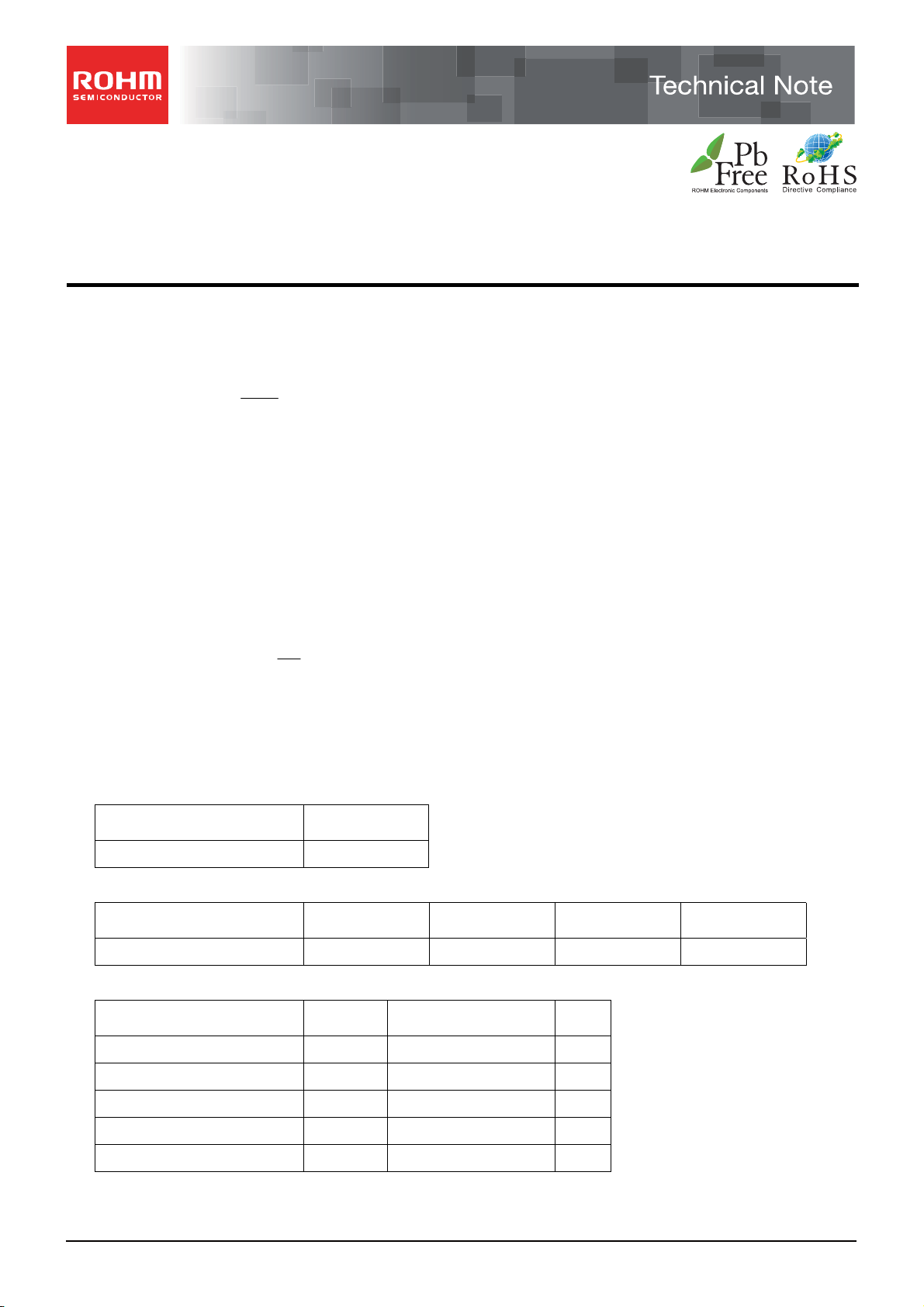
●Sync data input / output timing
tCSS
tCS
CS
SCK
SI
SO
tSCKS
tSCKWH
tSCKWL
tDIS
tDIH
High-Z
Fig.1 Input timing
tRC
tFC
SI is taken into IC inside in sync with data rise edge of SCK.
IInput address and data from the most significant bit MSB.
CS
SCK
SI
SO
tPD
tOH
Fig.2 Input / Output timing
tRO,tFO
tCSH
tSCKH
tOZ
tCS
h-Z
Hi
SO is output in sync with data fall edge of SCK. Data is
output from the most significant bit MSB.
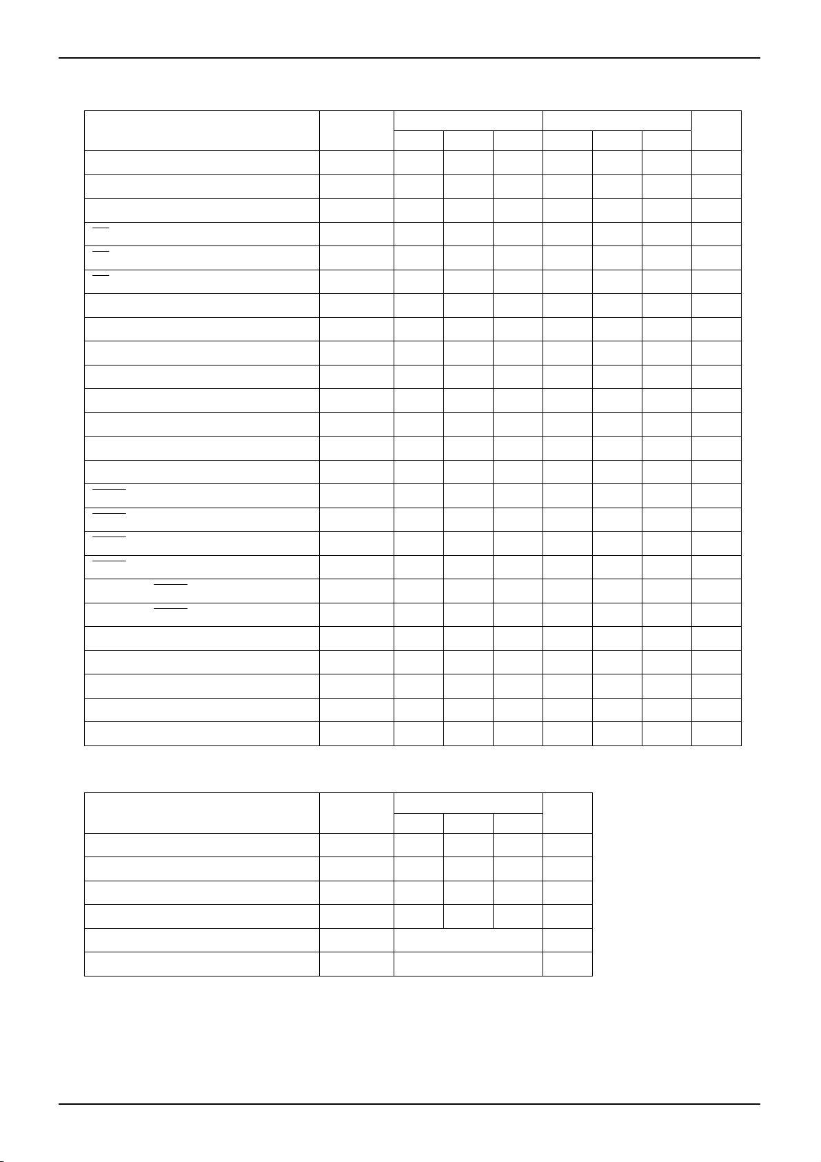
●Block diagram
CS
SCK
INSTRUCTION DECODE
CONTROL CLOCK
GENE RATI ON
SI
HOLD
INSTRUCTION
REGISTER
WPB
SO
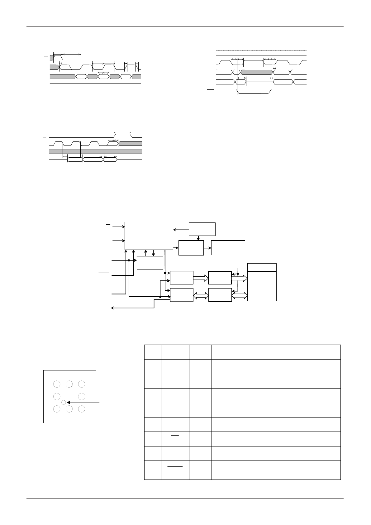
●Pin assignment and description
VOLTAGE
DETE CTIO N
WRITE
INHIBITION
ADDRESS
REGISTER
DATA
REGISTER
Fig.4 Block diagram
Land
No.
Terminal
name
Input/
Output
A1 WPB Input
"H"
CS
"L"
SCK
SI
SO
HOLD
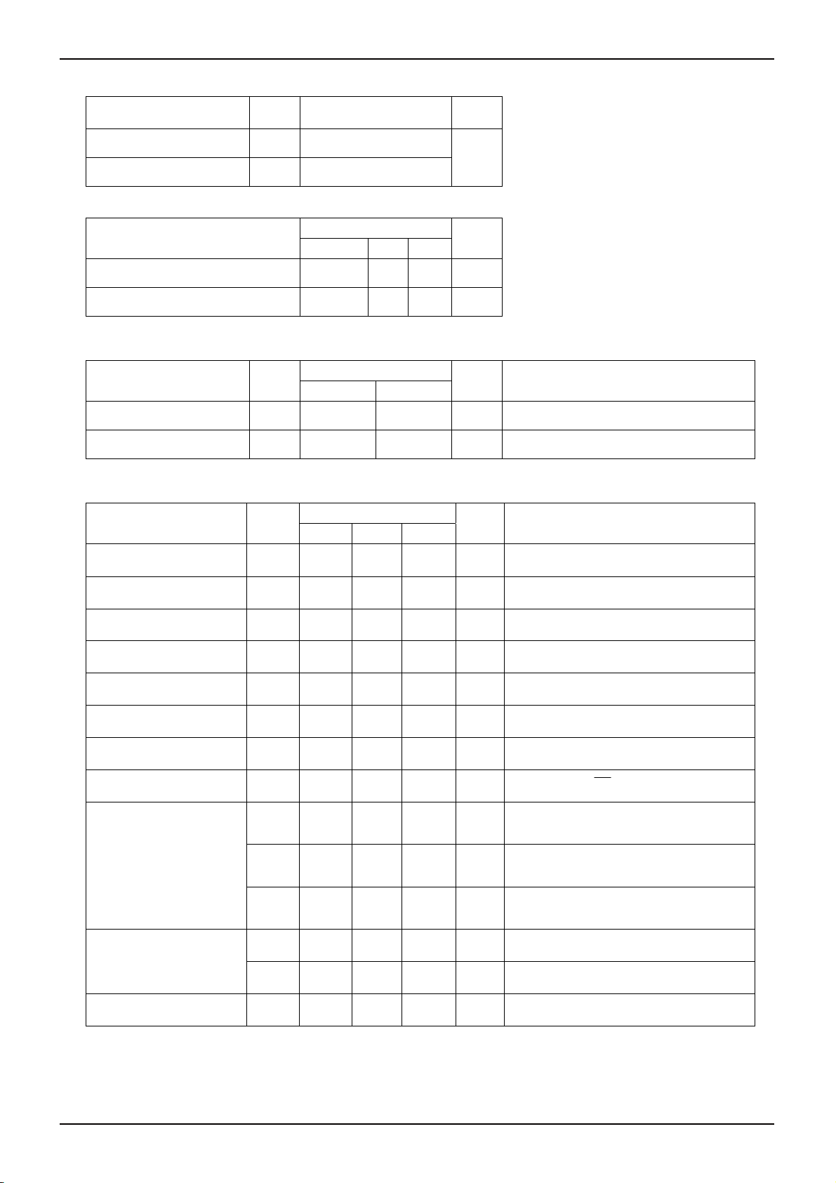
n+1
Dn+1
tHFS tHFH
tHOZ
Dn
High-Z
tHRS tHRH
tDIS
n
tHPD
Dn Dn-1
Fig.3 HOLD timing
HIGH VOLTAGE
GENERATOR
STATUS R EGISTER
ADDRESS
11b it
DECO DER
READ/WRITE
AMP
11bit
1~64K
EEPROM
8bit 8bit
Function
Write protect input
Write status register command is prohibited.
Technical Note
n-1
C
B
C1
C2 C3
B1 B3
A2 GND – All input / output reference voltage, 0V
A3 SI Input Start bit, ope code, address, and serial data input
INDEX post
3
2
1
3
Fig.5 Pin assignment diagram
B1 SO Output Serial data output
B3 SCK Input Serial clock input
C1 CS Input Chip select input
C2 Vcc – Power source to be connected
Hold input
C3 HOLD Input
Command communication may be
suspended temporarily (HOLD status)
www.rohm.com
© 2010 ROHM Co., Ltd. All rights reserved.
4/18
2010.10 - Rev.
A
BU9832GUL-W
K
●Characteristic data (The following characteristic data are Typ. Values.)
6
Ta=-40℃
5
Ta=25℃
Ta=85℃
4
IOH[mA]
SPEC
Vcc[V]
Vcc[V]
SPEC
Vcc[V]
Vcc[V]
SPEC
Ta=-40℃
Ta=25℃
Ta=85℃
Ta=-40℃
Ta=25℃
Ta=85℃
SPEC
SPEC
3
VIH[V]
2
1
0
0123456
Fig.6 "H" input voltege VIH(CS,SCK,SI,HOLD,WP) Fig.7 "L" input voltage VIL(CS,SCK,SI,HOLD,WP)
2
1.8
1.6
VOH[V]
SPEC
1.4
1.2
0 0.4 0.8 1.2
Fig.9 "H" output voltage VOH-IOH (Vcc=1.8V)
1.5
1
Ta=-40℃
ILI[μA]
Ta=25℃
Ta=85℃
0.5
0
0123456
Fig.12 Input leak current ILI(CS,SCK,SI,HOLD,WP)
2.5
fSK=5MHz
DATA=55h
2
1.5
Ta=-40℃
Ta=25℃
1
ICC4,5[mA]
Ta=85℃
0.5
0
0123456
Fig.15 Consumption current at READ operation
ICC4,5(READ,WRSR,fSK=5MHz)
250
200
150
100
tSCKWH[ns]
50
SPEC
0
0123456
Fig.18 tSCK high time tSCKWH Fig.20 CS high time tCS
6
Ta=-40℃
5
Ta=25℃
Ta=85℃
4
3
VIL[V]
2
1
0
0123456
1
Ta=-40℃
0.8
Ta=25℃
Ta=85℃
0.6
VOL[V]
0.4
0.2
0
0123456
Fig.10 "L" output voltage VOL-IOL (Vcc=2.5V)
1.5
1
Ta=-40℃
Ta=25℃
Ta=85℃
ILO[μA]
0.5
0
0123456
Fig.13 Output leak current ILO(SO)
2.5
2
Ta=-40℃
1.5
Ta=25℃
Ta=85℃
ISB[μA]
1
0.5
0
0123456
Fig.16 Consumption current at standby operation ISB
250
200
150
100
tSCKWL[ns]
50
0
0123456
Vcc[V]
SPEC
IOL[mA]
SPEC
Vcc[V]
SPEC
Fig.19 tSCK low time tSCKWL
Vcc[V]
Vcc[V]
Ta=-40℃
Ta=25℃
Ta=85℃
SPEC
SPEC
SPEC
Technical Note
1
Ta=-40℃
0.8
Ta=25℃
Ta=85℃
0.6
VOL[V]
0.4
SPEC
0.2
0
0123456
Fig.8 "L" output voltage VOL-IOL (Vcc=1.8V)
2.6
2.4
2.2
VOH[V]
SPEC
2
1.8
0 0.4 0.8 1.2
Fig.11 "H" output voltage VOH-IOH (Vcc=2.5V)
4
fSK=5MHz
DATA=55h
3
2
ICC1,2,3[mA]
1
0
0123456
Fig.14 Current consumption at WRITE operation
ICC1,2,3 (WRITE,PAGE WRITE,W RSR,fSCK=5MHz)
100
10
fSCK[MHz]
1
0.1
0123456
250
200
150
tCS[ns]
100
50
0
0123456
IOL[mA]
Ta=-40℃
Ta=25℃
Ta=85℃
IOH[mA]
Ta=-40℃
Ta=25℃
Ta=85℃
SPEC
Vcc[V]
SPEC
SPEC
Fig.17 SCK frequency fSC
SPEC
Vcc[V]
Vcc[V]
Ta=-40℃
Ta=25℃
Ta=85℃
Ta=-40℃
Ta=25℃
Ta=85℃
SPEC
SPEC
www.rohm.com
© 2010 ROHM Co., Ltd. All rights reserved.
5/18
2010.10 - Rev.
A
BU9832GUL-W
●Characteristic data (The following characteristic data are Typ. Values.)
250
Vcc[V]
SPEC
Vcc[V]
Ta=-40℃
Ta=25℃
Ta=85℃
SPEC
200
150
100
tCSS[ns]
50
0
-50
60
50
40
30
tDIH[ns]
20
10
0
SPEC
0123456
Fig.21 CS setup time tCSS
SPEC
Ta=-40℃
Ta=25℃
Ta=85℃
0123456
Fig.24 SI hold time tDIH
250
Vcc[V]
Vcc[V]
Ta=-40℃
Ta=25℃
Ta=85℃
SPEC
Ta=-40℃
Ta=25℃
Ta=85℃
SPEC
tPD
200
150
100
tCSH[ns]
50
0
200
150
100
tPD1[ns]
50
0
Fig.25 Data output delay time
SPEC
0123456
Fig.22 CS hold time tCSH
SPEC
0123456
300
SPEC
Vcc[V]
SPEC
Vcc[V]
SPEC
Ta=-40℃
Ta=25℃
Ta=85℃
Ta=-40℃
Ta=25℃
Ta=85℃
Ta=-40℃
Ta=25℃
Ta=85℃
250
200
150
tOZ[ns]
100
50
0
300
250
200
150
tHOZ[ns]
100
50
0
120
90
60
tFO[ns]
30
SPEC
0123456
Fig.27 Output disable time tOZ Fig.28 HOLD setting hold time tHFH Fig.29 HOLD release hold time tHRH
SPEC
CS
0123456
Fig.30 Time From HOLD to output High-Z tHOZ
SPEC
140
120
100
80
60
tHFH[ns]
40
20
0
-20
0123456
160
120
80
tHPD[ns]
40
0
-40
10
8
6
4
tE/W[ms]
2
SPEC
CS
0123456
Fig.31 Time from HOLD to output change tHPD
SPEC
SPEC
Vcc[V]
SPEC
SPEC
Vcc[V]
Ta=-40℃
Ta=25℃
Ta=85℃
Ta=-40℃
Ta=25℃
Ta=85℃
Ta=-40℃
Ta=25℃
Ta=85℃
0
0123456
Vcc[V]
Fig.33 Output fall time tFO
0
0123456
Fig.34 Write cycl e time tE/W
Vcc[V]
1(CL=100pF)
Technical Note
60
SPEC
Vcc[V]
Vcc[V]
SPEC
SPEC
Ta=-40℃
Ta=25℃
Ta=85℃
SPEC
Vcc[V]
Vcc[V]
Ta=-40℃
Ta=25℃
Ta=85℃
Ta=-40℃
Ta=25℃
Ta=85℃
Ta=-40℃
Ta=25℃
Ta=85℃
40
20
tDIS[ns]
0
-20
-40
200
150
100
tPD2[ns]
50
0
0123456
Fig.26 Data output delay time tPD2(CL=30pF)
150
120
90
60
tHRH[ns]
30
0
-30
120
90
60
tRO[ns]
30
0
SPEC
0123456
Fig.23 SI setup time tDIS
SPEC
SPEC
0123456
SPEC
CS
0123456
Fig.32 Output rise time tRO
www.rohm.com
© 2010 ROHM Co., Ltd. All rights reserved.
6/18
2010.10 - Rev.

A
BU9832GUL-W
Technical Note
●Features
○Status registers
This IC has status registers. The status registers are of 8 bits and express the following parameters.
BP0 and BP1 can be set by write status register command. These 2 bits are memorized into the EEPROM, therefore are
valid even when power source is turned off.
Rewrite characteristics and data hold time are same as characteristics of the EEPROM.
WEN can be set by write enable command and write disable command. WEN becomes write disable status when power
source is turned off. R
―
/B is for write confirmation, therefore cannot be set externally.
The value of status register can be read by read status command.
●Status registers
Product number bit 7 bit 6 bit 5 bit 4 bit 3 bit 2 bit 1 bit 0
BU9832GUL-W
bit
Memory
location
WPEN EEPROM
BP1
BP0
EEPROM
WEN Register
R―/B Register
●Write disable block setting
BP1 BP0 Write disable block
0 0 None
WPEN 0 0 0 BP1 BP0 WEN R―/B
Function Contents
WP pin enable / disable designation bit
WPEN=0=invalid
WPEN=1=valid
This enables / disables the functions of
pin.
This designates the write disable area of
EEPROM write disable block designation bit
EEPROM. Write designation areas of product
numbers are shown below.
Write and write status register write
enable / disable status confirmation bit
WEN=0=prohibited
WEN=1=permitted
Write cycle status (READY / BUSY) status
confirmation bit
B/R =0=READY
B/R =1=BUSY
WP
0 1 300h-3FFh
1 0 200h-3FFh
1 1 000h-3FFh
○
WP pin
By setting
WP =LOW, write command is prohibited. As for BU9832GUL-W when WPEN bit is set “1”, the WP pin
functions become valid. And the write command to be disabled at this moment is WRSR.
However, when write cycle is in execution, no interruption can be made.
Product number WRSR WRITE
BU9832GUL-W Prohibition possible but WPEN bit “1” Prohibition impossible
HOLD pin
○
By
HOLD pin, data transfer can be interrupted. When SCK=”1”, by making HOLD from “1” into”0”, data transfer to
EEPROM is interrupted. When SCK = “0”, by making
HOLD from “0” into “1”, data transfer is restarted.
www.rohm.com
© 2010 ROHM Co., Ltd. All rights reserved.
7/18
2010.10 - Rev.

A
BU9832GUL-W
―
Technical Note
●Command mode
Command Contents Ope code
WREN Write enable Write enable command 0000 0110
WRDI Write disable Write disable command 0000 0100
READ Read Read command 0000 0011
WRITE Write Write command 0000 0010
RDSR Read status register Status register read command 0000 0101
WRSR Write status register Status register write command 0000 0001
●Timing chart
1. Write enable (WREN) / disable (WRDI) cycle
・WREN (WRITE ENABLE): Write enable
―――
CS
CS
SCK
SI
SO
00 0 0 0110
High-Z
603 712 45
Fig.35 Write enable command
・WRDI (WRITE DISABLE): Write disable
――
CS
CS
SCK
0312 4
5
7
6
SO
00 0 0SI0100
High-Z
Fig.36 Write disable
○This IC has write enable status and write disable status. It is set to write enable status by write enable command, and it
is set to write disable status by write disable command. As for these commands, set
CS LOW, and then input the
respective ope codes. The respective commands accept command at the 7-th clock rise. Even with input over 7 clocks,
command becomes valid.
When to carry out write and write status register command, it is necessary to set write enable status by the write enable
command. If write or write status register command is input in the write disable status, commands are cancelled. And
even in the write enable status, once write and write status register command is executed once, it gets in the write
disable status. After power on, this IC is in write disable status.
www.rohm.com
© 2010 ROHM Co., Ltd. All rights reserved.
8/18
2010.10 - Rev.

A
BU9832GUL-W
A
A0A
Technical Note
2. Read command (READ)
CS
SCK
SI
0 3 71 2
0 0 0 0 0
High-Z
4 5
6 8
1 1 0
~
~
~ ~
~ ~
**
*
~ ~
~ ~
~ ~
~ ~
23 3024
~ ~
9
1
~ ~
~ ~
~ ~
~ ~
~ ~
~ ~
~ ~
D6SO
D7
D2 D1
D0
*=Don't Care
Fig.37 Read command
By read command, data of EEPROM can be read. As for this command, set CS LOW, then input address after read ope
code. EEPROM starts data output of the designated address. Data output is started from SCK fall of 15
clock, and from D7
to D0 sequentially. This IC has increment read function. After output of data for 1 byte (8bits), by continuing input of SCK,
data of the next address can be read. Increment read can read all the addresses of EEPROM. After reading data of the
most significant address, by continuing increment read, data of the most insignificant address is read.
3. Write command (WRITE)
CS
SCK
SI
SO
1 2 4
0 3 7 85 6
0 0 0 0 0
High-Z
~
~
~
~
~
~
~
~
~
* *
A9
~
~
~
~
~
1
0
0
*
23 3024
~
~
A0A1
~
~
~
~
~
~
D6
~
~
~
~
31
D2 D1D7
D0
*=Don't Care
Fig.38 Write command
By write command, data of EEPROM can be written. As for this command, set
after write ope code. Then, by making
CS HIGH, the EEPROM starts writing. The write time of EEPROM requires time of
tE/W (Max 5ms). During tE/W, other than status read command is not accepted. Start
CS LOW, then input address and data
CS after taking the last data (D0),
and before the next SCK clock starts. At other timing, write command is not executed, and this write command is cancelled.
This IC has page write function, and after input of data for 1 byte (8 bits), by continuing data input without starting
data up to 16 bytes can be written for one tE/W. In page write, the insignificant 4
bit of the designated address is
incremented internally at every time when data of 1 byte is input and data is written to respective addresses. When data of
the maximum bytes or higher is input, address rolls over, and previously input data is overwritten.
CS ,
www.rohm.com
© 2010 ROHM Co., Ltd. All rights reserved.
9/18
2010.10 - Rev.

A
BU9832GUL-W
8
5
5
Technical Note
4. Status register write / read command
CS
1 2
4
6
SCK
0 3 7
SI
SO
0 0 0 0 1
Hi gh -Z
0
0
0
9 10 11 12 13 14 1
bit7 bit6 bit5 bit4 bit3 bit2 bit1 bit0
WPEN
* * BP1 BP 0 **
*
*=Don't care
Fig.39 Status register write command
Write status register command can write status register data. The data can be written by this command are 2 bits
BP1 (bit3) and BP0 (bit2) among 8 bits of status register. By BP1 and BP0, write disable block of EEPROM can be set. As
for this command, set
EEPROM starts writing. Write time requires time of tE/W as same as write. As for
CS LOW, and input ope code of write status register, and input data. Then, by making CS HIGH,
CS rise, start CS after taking the last
data bit (bit0), and before the next SCK clock starts. At other timing, command is cancelled. Write disable block is
determined by BP1 and BP0, and the block can be selected from 1/4 of memory array, 1/2, and entire memory array.
(Refer to the write disable block setting table.) To the write disabled block, write cannot be made, and only read can be
made.
*1 3bits including 1WPEN (bit7)
CS
SCK
5 12
4 8
SI
0
0 0 0
0
1 1
SO
High-Z
11 15 3 7 9
1060
13
14 1 2
0
bit7 bit6 bit5 bit4
WPEN
00 BP00 BP1
bit3 bit2 bit1 bit0
WEN
R/B
Fig.40 Status register read command
* 1
, that is,
www.rohm.com
© 2010 ROHM Co., Ltd. All rights reserved.
10/18
2010.10 - Rev.

A
BU9832GUL-W
Technical Note
●At standby
○Current at standby
Set CS “H”, and be sure to set SCK, SI, WP ,HOLD input “L” or “H”. Do not input intermediate electric potantial.
○Timing
As shown in Fig.41, at standby, when SCK is “H”, even if
at SCK rise edge after fall of
CS . At standby and at power ON/OFF, set CS “H” status.
―――
CS
SCK
―――
Even if CS
SI status is not read at that edge.
Command start here. SI is read.
0 1 2
CS is fallen, SI status is not read at fall edge. SI status is read
is fallen at SCK=SI=”H”,
SI
Fig.41 Operating timing
●
WP cancel valid area
WP is normally fixed to “H” or “L” for use, but when WP is controlled so as to cancel write status register command and
write command, pay attention to the following
While write or write status register command is executed, by setting
cancelled. The area from command ope code before
area. However, once write is started, any input cannot be cancelled.
WP valid timing.
WP = “L” in cancel valid area, command can be
CS rise at internal automatic write start becomes the cancel valid
WP input becomes Don’t Care, and cancellation
becomes invalid.
SCK
15 16
Ope Code Data
WP cancel invalid area
CS
tE/W
Data write tim e
WP cancel invalid area
Fig.42
WP valid timing (WRSR)
Ope Code
Address
WP cancel inv alid area
Data
tE /W
Da ta wr ite tim e
WP cancel in valid area
Fig.43 WP valid timing (WRITE)
●
HOLD pin
By HOLD pin, command communication can be stopped temporarily (HOLD status). The HOLD pin carries out command
communications normally when it is HIGH. To get in HOLD status, at command communication, when SCK=LOW, set the
HOLD pin LOW. At HOLD status, SCK and SI become Don’t Care, and SO becomes high impedance (High-Z). To release
the HOLD status, set the
HOLD pin HIGH when SCK=LOW. After that, communication can be restarted from the point
before the HOLD status. For example, when HOLD status is made after A5 address input at read, after release of HOLD
status, by starting A4 address input, read can be restarted. When in HOLD status, leave
CS LOW. When it is set
CS =HIGH in HOLD status, the IC is reset, therefore communication after that cannot be restarted.
www.rohm.com
© 2010 ROHM Co., Ltd. All rights reserved.
11/18
2010.10 - Rev.
A
BU9832GUL-W
●Method to cancel each command
○READ
・Method to cancel : cancel by
CS = “H”
○RDSR
・Method to cancel : cancel by
CS = “H”
○WRITE, PAGE WRITE
a: Ope code, address input area.
Cancellation is available by
CS =”H”
b: Data input area (D7~D1 input area)
Cancellation is available by
CS =”H”
c: Data input area (D0 area)
When
After
CS is started, write starts.
CS rise, cancellation cannot be made by any means.
d: tE/W area.
Cancellation is available by
starts (
CS is started) in the area c, cancellation cannot be
CS = “H”. However, when write
made by any means. And by inputting on SCK clock,
cancellation cannot be made. In page write mode, there is
write enable area at every 8 clocks.
Note 1) If Vcc is made OFF during write execution, designated address data is not guaranteed, therefore write it once again.
Note 2) If
CS is started at the same timing as that of the SCK rise, write execution / cancel becomes unstable,therefore,
it is necessary to fall in SCK = “L” area. As for SCK rise, assure timing of tCSS / tCSH or higher.
○WRSR
a: From ope code to 15 rise.
Cancel by
CS =”H”.
b: From 15 clock rise to 16 clock rise (write enable area).
When
After
CS is started, write starts.
CS rise, cancellation cannot be made by any means.
c: After 16 clock rise.
Cancel by
CS =”H”. However, when write starts ( CS is started)
in the area b, cancellation cannot be made by any means.
And, by inputting on SCK clock, cancellation cannot be made.
Note 1) If Vcc is made OFF during write execution, designated address data is not guaranteed, therefore write it once again
Note 2) If
CS is started at the same timing as that of the SCK rise, write execution / cancel becomes unstable, therefore, it is
necessary to fall in SCK = “L” area. As for SCK rise, assure timing of tCSS / tCSH or higher.
○WREN/WRDI
a: From ope code to clock rise, cancel by
b: Cancellation is not available when
CS is started after 7 clock.
CS = “H”.
Ope code Address
8 bits 8 bits 8 bits
Cancel available in all areas of read mode
Fig.44 READ cancel valid timing
Ope code
8 bits 8 bits
Cancel available in all
areas of rdsr mode
Fig.45 RDSR cancel valid timing
Ope code
8bits 8bits 8bits
Address
a
Fig.46 WRITE cancel valid timing
SCK
D7 bD6 D5 D4 D3 D2 D1 D0
SI
Ope code Address
8 bits
SCK
SI
a
Fig.47 WRSR cancel valid timing
SCK
Fig.48 WREN/WRDI cancel valid timing
Technical Note
Data
Data
tE/W
Data(n)
b d
14 15 16 17
D1 D0
a b c
8 bits
b
7 8 9
b
a
Ope code
8 bits
a b
c
c
tE/W
c
www.rohm.com
© 2010 ROHM Co., Ltd. All rights reserved.
12/18
2010.10 - Rev.
A
BU9832GUL-W
3
3
Technical Note
●High speed operation
In order to realize stable high speed operations, pay attention to the following input / output pin conditions.
○Input pin pull up, pull down resistance
When to attach pull up, pull down resistance to EEPROM input pin, select an appropriate value for the microcontroller V
I
OL
from V
characteristics of this IC.
IL
○Pull up resistance
Microcontroller
“L” output “L” input
I
EEPROM
OLM
OLM
R
PU
Fig.49 Pull up resistance
≥
R
PU
V
OLM
V
V
ILE
Example) When Vcc=5V, V
from the equation ①,
RPU≥
∴RPU≥ 2.3[kΩ]
VCC-V
≤ V
I
OLM
ILE
=1.5V, V
ILM
5-0.4
2×10
OLM
-
・・・①
・・・②
OLM
=0.4V, I
=2mA,
OLM
With the value of RPU to satisfy the above equation, V
0.4V or higher, and with V
(=1.5V), the equation ② is also satisfied.
ILE
・V
・V
・I
:EEPROM V
ILM
:Microcontroller VOL specifications
OLM
:Microcontroller IOL specifications
OLM
specifications
IH
And, in order to prevent malfunction, mistake write at power ON/OFF, be sure to make CS pull up.
○Pull down resistance
V
=5V, V
OHM
I
OHM
IHE
OHM=VCC
-0.5V, I
・・・③
・・・④
OHM
=0.4mA,
×0.7V, from the equation③,
5-0.5
-
0.4×10
OHM
EEPROM
V
IHE
V
I
Fig.50 Pull down resistance
OHM
Example) When V
RPD≥
V
OHM
V
IHM=VCC
≥ V
CC
R
≥
PD
∴RPU≥ 11.3[kΩ]
Further, by amplitude VIHE, VILE of signal input to EEPROM, operation speed changes. By inputting signal of amplitude
/ GND level to input, more stable high speed operations can be realized. On the contrary, when amplitude of 0.8VCC
of V
CC
/ 0.2Vcc is input, operation speed becomes slow.
In order to realize more stable high speed operation, it is recommended to make the values of R
possible, and make the amplitude of signal input to EEPROM close to the amplitude of V
ж
(
1 At this moment, operating timing guaranteed value is guaranteed.)
80
70
60
50
40
tPD[ns]
30
20
10
0
0 0.2 0.4 0.6 0.8 1
Fig.51 V
IL
ж1
tPD_VIL characteristics
Spec
Vcc =2.5V
Ta=25
℃
VIH= Vcc
=100pF
C
L
VIL[V]
dependency of data output delay time
/ GND level.
CC
, RPD as large as
PU
becomes
OLM
OL
,
www.rohm.com
© 2010 ROHM Co., Ltd. All rights reserved.
13/18
2010.10 - Rev.

A
BU9832GUL-W
Technical Note
○SO load capacity condition
Load capacity of SO output pin affects upon delay characteristic of SO output. (Data output delay time, time from
to High-Z) In order to make output delay characteristic into higher speed, make SO load capacity small. In concrete, “Do
not connect many devices to SO bus”, “Make the wire between the controller and EEPROM short”, and so forth.
80
VIH/VIL=0.8Vcc/0.2V cc
70
60
50
tPD[ns]
40
30
tPD-CL characteristics
Vcc =2.5V Ta=25
Spec
℃
Spec
EEPROM
SO
CL
20
0 20 40 60 80 100 120
CL[pF]
Fig.52 SO load dependency of data output delay time
○Other cautions
Make the wire length from the microcontroller to EEPROM input signal same length, in order to prevent setup / hold
violation to EEPROM, owing to difference of wire length of each input.
HOLD
www.rohm.com
© 2010 ROHM Co., Ltd. All rights reserved.
14/18
2010.10 - Rev.

A
BU9832GUL-W
●Equivalent circuit
○Output circuit
○Input circuit
SCK
Fig.55 SCK input equivalent circuit
――――――
HOLD
Fig.57
OEint.
Fig.53 SO output equivalent circuit
―――
CS
RESET
int.
Fig.54 CS input equivalent circuit
SI
Fig.56 SI input equivalent circuit
―――
WP
HOLD input equivalent circuit Fig.58
Technical Note
SO
WP
input equivalent circuit
www.rohm.com
© 2010 ROHM Co., Ltd. All rights reserved.
15/18
2010.10 - Rev.

A
BU9832GUL-W
t
ad example
G
cc
Technical Note
●Notes on power ON/OFF
○At power ON/OFF, set
When
CS is “L”, this IC gets in input accept status (active). If power is turned on in this status, noises and the likes may
cause malfunction, mistake write or so. To prevent these, at power ON, set
CS “H” (=Vcc).
CS “H”. (When CS is in “H” status, all
inputs are canceled.)
Vcc
V
ND
Vcc
CS
GND
Good example
B
Fig.59 CS timing at power ON/OFF
(Good example)
CS terminal is pulled up to Vcc.
At power OFF, take 10ms or higher before supply. If power is turned on without observing this condition,
the IC internal circuit may not be reset, which please note.
(Bad example)
CS terminal is “L” at power ON/OFF.
In this case,
CS always becomes “L” (active status), and EEPROM may have malfunction, mistake
write owing to noises and the likes.
Even when
CS input is High-Z, the status becomes like this case, which please note.
○P.O.R. circuit
This IC has a P.O.R. (Power On Reset) circuit as mistake write countermeasure. After P.O.R. action, it gets in write disable
status. The P.O.R. circuit is valid only when power is ON, and does not work when power is OFF. When power is ON, if the
recommended conditions of the following tR, tOFF, and Vbot are not satisfied, it may become write enable status owing to
noises and the likes.
Vcc
0
Fig.60 Rise waveform
tOFF
tR
Vbo
Recommended conditions of tR, t
tR t
10ms or below 10ms or higher 0.3V or below
, Vbot
OFF
Vbot
OFF
100ms or below 10ms or higher 0.2V or below
●Noise countermeasures
○Vcc noise (bypass capacitor)
When noise or surge gets in the power source line, malfunction may occur, therefore, for removing these, it is
recommended to attach a bypass capacitor (0.1µF) between IC Vcc and GND. At that moment, attach it as close to IC as
possible. And, it is also recommended to attach a bypass capacitor between board Vcc and GND.
○SCK noise
When the rise time (tR) of SCK is long, and a certain degree or more of noise exists, malfunction may occur owing to clock
bit displacement. To avoid this, a Schmitt trigger circuit is built in SCK input. The hysterisis width of this circuit is set about
0.2V, if noises exist at SCK input, set the noise amplitude 0.2Vp-p or below. And it is recommended to set the rise time (tR)
of SCK 100ns or below. In the case when the rise time is 100ns or higher, take sufficient noise countermeasures. Make the
clock rise, fall time as small as possible.
WP noise
○
During execution of write status register command, if there exist noises on
and forcible cancellation may result, which please note. To avoid this, a Schmitt trigger circuit is built in
same manner, a Schmitt trigger circuit is built in SI input, SI input and
WP pin, mistake in recognition may occur
WP input. In the
HOLD input too.
www.rohm.com
© 2010 ROHM Co., Ltd. All rights reserved.
16/18
2010.10 - Rev.

A
BU9832GUL-W
●Notes for use
(1) Described numeric values and data are design representative values, and the values are not guaranteed.
(2) We believe that application circuit examples are recommendable, however, in actual use, confirm characteristics further
sufficiently. In the case of use by changing the fixed number of external parts, make your decision with sufficient margin in
consideration of static characteristics and transition characteristics and fluctuations of external parts and our LSI.
(3) Absolute maximum ratings
If the absolute maximum ratings such as impressed voltage and operating temperature range and so forth are exceeded,
LSI may be destructed. Do not impress voltage and temperature exceeding the absolute maximum ratings. In the case of
fear exceeding the absolute maximum ratings, take physical safety countermeasures such as fuses, and see to it that
conditions exceeding the absolute maximum ratings should not be impressed to LSI.
(4) GND electric potential
Set the voltage of GND terminal lowest at any action condition. Make sure that each terminal voltage is higher than that of
GND terminal.
(5) Heat design
In consideration of permissible dissipation in actual use condition, carry out heat design with sufficient margin.
(6) Terminal to terminal short circuit and wrong packaging
When to package LSI onto a board, pay sufficient attention to LSI direction and displacement. Wrong packaging may
destruct LSI. And in the case of short circuit between LSI terminals and terminals and power source, terminal and GND
owing to foreign matter, LSI may be destructed.
(7) Use in a strong electromagnetic field may cause malfunction, therefore, evaluate design sufficiently.
Technical Note
www.rohm.com
© 2010 ROHM Co., Ltd. All rights reserved.
17/18
2010.10 - Rev.

A
BU9832GUL-W
●Ordering part number
B U 9 8 3 2 G U L - W E 2
Technical Note
Part No. Part No. Package
VCSP50L2
(BU9832GUL-W)
1PIN MARK
8-φ0.25±0.05
0.05
(φ0.15)INDEX POST
0.545±0.1
2.09±0.1
BA
C
B
A
P=0.5×2
0.08 S
A
321
1.85±0.1
0.55MAX
0.1±0.05
S
0.425±0.1
B
P=0.5×2
(Unit : mm)
GUL : VCSP50L2
<Tape and Reel information>
Embossed carrier tapeTape
Quantity
Direction
of feed
3000pcs
E2
The direction is the 1pin of product is at the upper left when you hold
()
reel on the left hand and you pull out the tape on the right hand
Reel
W-CELL Packaging and forming specification
E2: Embossed tape and reel
1pin
Order quantity needs to be multiple of the minimum quantity.
∗
Direction of feed
www.rohm.com
© 2010 ROHM Co., Ltd. All rights reserved.
18/18
2010.10 - Rev.

Notes
No copying or reproduction of this document, in par t or in whole, is permitted without the
consent of ROHM Co.,Ltd.
The content specied herein is subject to change for improvement without notice.
The content specied herein is for the purpose of introducing ROHM's products (hereinafter
"Products"). If you wish to use any such Product, please be sure to refer to the specications,
which can be obtained from ROHM upon request.
Examples of application circuits, circuit constants and any other information contained herein
illustrate the standard usage and operations of the Products. The peripheral conditions must
be taken into account when designing circuits for mass production.
Great care was taken in ensuring the accuracy of the information specied in this document.
However, should you incur any damage arising from any inaccuracy or misprint of such
information, ROHM shall bear no responsibility for such damage.
The technical information specied herein is intended only to show the typical functions of and
examples of application circuits for the Products. ROHM does not grant you, explicitly or
implicitly, any license to use or exercise intellectual property or other rights held by ROHM and
other parties. ROHM shall bear no responsibility whatsoever for any dispute arising from the
use of such technical information.
Notice
The Products specied in this document are intended to be used with general-use electronic
equipment or devices (such as audio visual equipment, ofce-automation equipment, communication devices, electronic appliances and amusement devices).
The Products specied in this document are not designed to be radiation tolerant.
While ROHM always makes efforts to enhance the quality and reliability of its Products, a
Product may fail or malfunction for a variety of reasons.
Please be sure to implement in your equipment using the Products safety measures to guard
against the possibility of physical injury, re or any other damage caused in the event of the
failure of any Product, such as derating, redundancy, re control and fail-safe designs. ROHM
shall bear no responsibility whatsoever for your use of any Product outside of the prescribed
scope or not in accordance with the instruction manual.
The Products are not designed or manufactured to be used with any equipment, device or
system which requires an extremely high level of reliability the failure or malfunction of which
may result in a direct threat to human life or create a risk of human injur y (such as a medical
instrument, transportation equipment, aerospace machinery, nuclear-reactor controller, fuelcontroller or other safety device). ROHM shall bear no responsibility in any way for use of any
of the Products for the above special purposes. If a Product is intended to be used for any
such special purpose, please contact a ROHM sales representative before purchasing.
If you intend to export or ship overseas any Product or technology specied herein that may
be controlled under the Foreign Exchange and the Foreign Trade Law, you will be required to
obtain a license or permit under the Law.
Thank you for your accessing to ROHM product informations.
More detail product informations and catalogs are available, please contact us.
ROHM Customer Support System
www.rohm.com
© 2010 ROHM Co., Ltd. All rights reserved.
http://www.rohm.com/contact/
R1010
A
 Loading...