

Page 1

AIE Adaptive Image Enhancer Series
Video Encoders
built-in Image Correction
BU6520KV,BU6521KV
●Description
BU6520KV, BU6521KV are video encoders with built-in AIE image correcting function. Also, BU6521KV has the image
correcting function of the fog reduction, too.
Fog Reduction, the brightness correction, the backlight correction and the chroma emphasis can improve the visibility of the
input image of the camera.
* AIE and Fog Reduction function are image processing technology by ROHM’s hardware.
●Features
1) Format of video output is compatible with NTSC/PAL composite video format (CVBS).
Built-in DAC with direct 75Ω drive capability.
2) Built-in Fog Reduction function
3) Input/output data format is compatible with ITU-R BT.656 and YCbCr=4:2:2 with synchronization signal.
4) Compatible with NTSC (27MHz, 28.63636MHz and 19.06993MHz)/
PAL(27MHz, 28.375MHz, 35.46895MHz and 18.9375MHz)
5) Registers can be set up with a 2-line serial interface.
6) Registers can be automatically set up by reading from external EEPROM, when after resetting or changing mode.
*1 As for the Fog Reduction feature, it loads only BU6521KV.
*2 NTSC 19,06993 MHz and PAL 18,9375 MHz support only BU6521KV.
●Applications
Security camera, camera for automotive, drive recorder etc.
●Line up matrix
Part No.
BU6520KV
BU6521KV
Power Sopply
Voltage(V)
1.4 to 1.6
Core)
(V
DD
2.7 to 3.6
(VDDI/O, AVDD)
1.4 to 1.6
Core)
(V
DD
2.7 to 3.6
I/O, AVDD)
(V
DD
Image size
720x480,
SD size
720x480,
SD size
*1
, dynamic range correction, edge-emphasizing filter and gamma filter.
*2
.
Input
Interface
8bit,
YUV=4:2:2,
ITU-R BT.656
8bit,
YUV=4:2:2,
ITU-R BT.656
Control
Interface
2
C,
I
Serial
EEPROM
interface
2
C,
I
Serial
EEPROM
interface
Output
Interface
8bit,
YUV=4:2:2,
ITU-R BT.656
8bit,
YUV=4:2:2,
ITU-R BT.656
Feature
AIE,
Video output
AIE,
Fog reduction,
Video output
I2C BUS is a registered trademark of Philips
Temperature
No.10060ECT03
Operating
Range(℃)
-40 ~ +85 VQFP48C
-40 ~ +85 VQFP48C
Package
www.rohm.com
© 2010 ROHM Co., Ltd. All rights reserved.
1/18
2010.02 - Rev.C
Page 2

BU6520KV,BU6521KV
Technical Note
●Absolute maximum ratings
Parameter Symbol Rating Unit
Supply voltage1 (IO) VDDIO -0.3~+4.2 V
Supply voltage2 (IO) VDDI2C -0.3~+4.2 V
Supply voltage3 (DAC) AVDD -0.3~+4.2 V
Supply voltage4 (CORE) VDD -0.3~+2.1 V
Input voltage range VIN -0.3~IO_LVL+0.3 *1 V
Storage temperature range Tstg -40~+125 ℃
Power dissipation PD 400 *2, 900 *3 mW
*1 IO_LVL is a generic name of VDDIO, VDDI2C, and AVDD.
*2 IC only. In the case exceeding 25ºC, 4.0mW should be reduced at the rating 1ºC.
*3 When packaging a glass epoxy board of 70x70x1.6mm. If exceeding 25ºC, 9.0mW should be reduced at the rating 1ºC.
* Has not been designed to withstand radiation.
* Operation is not guaranteed at absolute maximum ratings.
●Operating conditions
Parameter Symbol Ratings Unit
Supply voltage 1 (IO) VDDIO 2.70 ~ 3.60 (Typ.: 3.30) V
Supply voltage 2 (IO) VDDI2C 2.70 ~ 3.60 (Typ.: 3.30) V
Supply voltage 3 (DAC) AVDD 2.70 ~ 3.60 (Typ.: 3.30) V
Supply voltage 4 (CORE) VDD 1.40 ~ 1.60 (Typ.: 1.50) V
Input voltage range VIN 0.00 ~ IO_LVL *1 V
Operating temperature range Topr -40 ~ +85 ºC
*1 IO_LVL is a generic name of VDDIO, VDDI2C, and AVDD.
* Please supply power source in order of VDD→(VDDIO, VDDI2C, and AVDD).
www.rohm.com
© 2010 ROHM Co., Ltd. All rights reserved.
2/18
2010.02 - Rev.C
Page 3
BU6520KV,BU6521KV
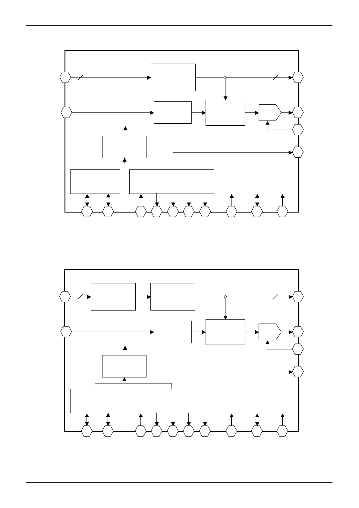
●Block Diagram
[BU6520KV]
Technical Note
CAMDI0
―CAMDI7
CAMHSI
CAMVSI
CAMCKI
[BU6521KV]
8
2-line Serial
Inter fac e
2
C)
(I
SDA SDC
Register
AIE
Tim ing
Genera tor
Serial
Interfac e
(SPI)
SDI SDO SCK SCEB
WPB
Fig.1 BU6520KV Block Diagram
8
Video
Encoder
RESETB TEST AU TO
10bit
DAC
MOD E0
MOD E1
CAMDO0
―CAMDO7
VOU T
IREF
CAMHSO
CAMVSO
CAMCKO
CAMDI0
―CAMDI7
CAMHSI
CAMVSI
CAMCKI
8
Fog reduction
2-line Serial
Inter fac e
2
(I
C)
SDA SDC
Register
AIE
Tim ing
Genera tor
Serial
Interfac e
(SPI)
SDI SDO SCK SCEB
WPB
Fig.2 BU6521KV Block Diagram
Vi de o
Encoder
RESETB TEST AUT O
10bit
DAC
8
MOD E0
MOD E1
CAMDO0
―CAMDO7
VOU T
IREF
CAMHSO
CAMVSO
CAMCKO
www.rohm.com
© 2010 ROHM Co., Ltd. All rights reserved.
3/18
2010.02 - Rev.C
Page 4

BU6520KV,BU6521KV
Technical Note
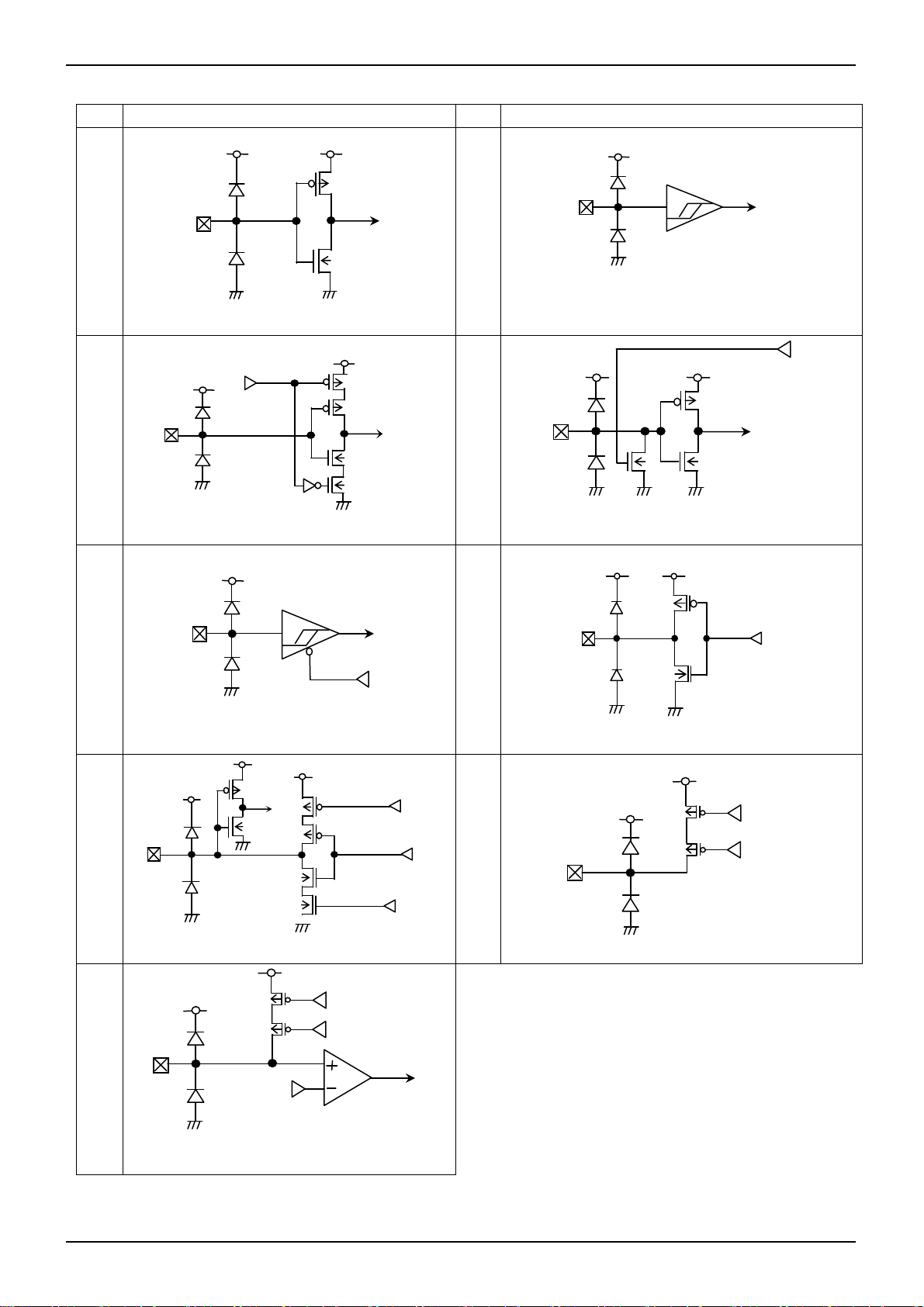
●Pin functional descriptions・Equivalent circuit
PIN
PIN Name In/Out
No.
Active
Level
Init Function explanation
Power
Source
System
1 SDI In DATA - SPI-bus data input 1 A
2 CAMDI7 In DATA - Data input bit 7 1 C
3 CAMDI6 In DATA - Data input bit 6 1 C
4 CAMDI5 In DATA - Data input bit 5 1 C
5 CAMDI4 In DATA - Data input bit 4 1 C
6 GND - GND - Common GROUND 1,2,4 -
7 VDD - PWR - CORE power source 4 -
8 CAMDI3 In DATA - Data input bit 3 1 C
9 CAMDI2 In DATA - Data input bit 2 1 C
10 CAMDI1 In DATA - Data input bit 1 1 C
11 CAMDI0 In DATA - Data input bit 0 1 C
12 CAMHSI In * - Horizontal timing input 1 C
I/O
type
*1
13 CAMVSI In * - Vertical timing input 1 C
14 CAMCKI In CLK - Clock input 1 E
15 GND - GND - Common GROUND 1,2,4 -
16 VDDIO - PWR - Digital IO power source 1 -
17 CAMDO0 Out DATA Low Data output bit 0 1 F
18 CAMDO1 Out DATA Low Data output bit 1 1 F
19 CAMDO2 Out DATA Low Data output bit 2 1 F
20 CAMDO3 Out DATA Low Data output bit 3 1 F
21 CAMDO4 Out DATA Low Data output bit 4 1 F
22 CAMDO5 Out DATA Low Data output bit 5 1 F
23 CAMDO6 Out DATA Low Data output bit 6 1 F
24 CAMDO7 Out DATA Low Data output bit 7 1 F
※ ” * ” in the Active Level column indicates that it may be changed during set-up of the register.
※ Init column indicates pin status when released from reset.
※ In the power system column, ” 1 ” stands for VDDIO, ” 2 ” stands for VDDI2C, ” 3 ” stands for AVDD, ” 4 ” stands for VDD.
*1 Fig.3 Equivalent Circuit Structures of input / output pins reference
www.rohm.com
© 2010 ROHM Co., Ltd. All rights reserved.
4/18
2010.02 - Rev.C
Page 5

BU6520KV,BU6521KV
Technical Note
PIN
PIN Name In/Out
No.
Active
Level
Init Function explanation
Power
Source
System
25 CAMHSO Out * Low Horizontal timing output 1 F
26 CAMVSO Out * Low Vertical timing output 1 F
27 CAMCKO Out CLK Low Clock output 1 F
28 GND - GND - Common GROUND 1,2,4 -
29 VDD - PWR - CORE power source 4 -
30 AUTO In High PD *2 Auto register setting enable signal 1 D
31 MODE0 In DATA PD *2 Auto register setting mode select bit 0 1 D
32 MODE1 In DATA PD *2 Auto register setting mode select bit 1 1 D
33 VOUT Out Analog - Analog composite output 3 H
34 AVSS - GND - Analog GROUND for DAC 3 -
35 IREF Out Analog - Reference voltage for DAC 3 I
36 AVDD - PWR - Analog power source for DAC 3 -
I/O
type
*1
37 GND - GND - Common GROUND 1,2,4 -
38 VDDI2C - PWR -
Digital IO power source
(For 2-line serial interface input/output)
2 -
39 SDA In/Out DATA In 2-line serial interface data input/output 2 G
40 SDC In/Out CLK In 2-line serial interface clock input 2 G
41 RESETB In Low - System reset signal 1 B
42 TEST In High PD *2 Test mode terminal (Connect to GND) 1 D
43 GND - GND - Common GROUND 1,2,4 -
44 VDDIO - PWR - Digital IO power source 1 -
45 WPB Out Low Low Write protect signal to EEPROM 1 F
46 SCEB Out Low High Chip select signal to EEPROM 1 F
47 SCK Out CLK Low SPI-bus clock 1 F
48 SDO Out DATA Low SPI-bus data output 1 F
※ ” * ” in the Active Level column indicates that it may be changed during set-up of the register.
※ Init column indicates pin status when released from reset.
※ In the power system column, ” 1 ” stands for VDDIO, ” 2 ” stands for VDDI2C, ” 3 ” stands for AVDD, ” 4 ” stands for VDD.
*1 Fig.3 Equivalent Circuit Structures of input / output pins reference
*2 Pull-down status.
www.rohm.com
© 2010 ROHM Co., Ltd. All rights reserved.
5/18
2010.02 - Rev.C
Page 6
BU6520KV,BU6521KV
Technical Note
Type Equivalent circuit configuration Typ Equivalent circuit configuration
A
Input terminal
VDDIO VDDIO
To internal
circuit
GND
GND
VDDIO
B
GND
Input terminal with hysteresis
To internal
circuit
VDDIO
Internal signal
VDDIO
C
GND
Input terminal with suspend
VDDIO
E
GND
Input terminal with hysteresis and suspend
G
VDDI2C
VDDI2C
To internal
circuit
GND
GND
GND
Input/Output terminal
GND
To internal
Internal signal
VDDI2C
Internal signal
Internal signal
Internal signal
To internal
circuit
circuit
VDDIO
D
GND
Input terminal with pull down
F
Output terminal
H
VOUT
VDDIO
GND
GND
AVDD
AVSS
VDDIO
VDDIO
AVDD
Internal signal
To internal
circuit
GND
Internal signal
GND
Internal signal
Internal signal
AVDD
AVDD
I
AVSS
Internal signal
IREF
Fig.3 Equivalent Circuit Structures of input / output pins
www.rohm.com
© 2010 ROHM Co., Ltd. All rights reserved.
Internal signal
Internal signal
To internal
circuit
6/18
2010.02 - Rev.C
Page 7

BU6520KV,BU6521KV
●Pin configrations
Technical Note
SDI
CAMDI7
CAMDI6
CAMDI5
CAMDI4
GND
VDD
CAMDI3
CAMDI2
CAMDI1
CAMDI0
CAMHSI
SCK
SDO
1
2
3
4
5
6
SCEB
WPB
GND
VDDIO
TEST
SDC
RESETB
VQFP48C
7
8
9
10
11
12
13 14 15 16 17 18 19 20 21 22 23 24
SDA
GND
VDDI2C
37383940414243444546 47 48
36
35
34
33
32
31
30
29
28
27
26
25
AVDD
IREF
AVSS
VOUT
MODE1
MODE0
AUTO
VDD
GND
CAMCKO
CAMVSO
CAMHSO
CAMVSI
CAMCKI
GND
VDDIO
CAMDO0
CAMDO1
Fig.4 Pin configrations
CAMDO2
CAMDO3
CAMDO4
CAMDO5
CAMDO6
CAMDO7
www.rohm.com
© 2010 ROHM Co., Ltd. All rights reserved.
7/18
2010.02 - Rev.C
Page 8

BU6520KV,BU6521KV
●Electrical characteristics(common)
(Unless otherwise specified VDD=1.50V, VDDIO=3.3V, VDDI2C=3.3V, AVDD=3.3V, GND=0.0V, Ta=25℃,f
Parameter Symbol
MIN. TYP. MAX.
Limits
Unit Condition
Input frequency fIN 2 - 35.5 MHz CAMCKI(DUTY45%~55%)
Technical Note
=35.5MHz)
IN
Supply current
(CORE)
Leakage current (CORE) IDDst1 - - 50 µA
Supply current
(DAC)
Leakage current (DAC) IDDst2 - - 5 µA
*1 Supply current(Total value of current of VDD, VDDIO, and VDDI2C) at color-bar image input in AIE enable and Digital output disable settings.
*2 Supply current(VDD) at color-bar image input in Fog-Reduction enable, AIE enable and Digital output disable settings.
BU6520KV IDD1 - 30 - mA 35.5MHz operational setting
BU6521KV IDD1 - 40 62 mA 35.5MHz operational setting*2
At sleep mode setting,
input terminal = GND setting
BU6520KV IDD2 - 38 - mA RL=37.5Ω, RIREF=2.4kΩ
BU6521KV IDD2 - 38 56 mA RL=37.5Ω, RIREF=2.4kΩ
input terminal=GND and
DAC power down mode setting
●Electrical characteristics(DC characteristics)
1. DC characteristics (IO)
(Unless otherwise specified VDD=1.50V, VDDIO=3.3V, VDDI2C=3.3V, AVDD=3.3V, GND=0.0V, Ta=25℃)
Parameter Symbol
MIN. TYP. MAX.
Limits
Unit Condition
Input ”H” current IIH -10 - 10 µA VIH=IO_LVL
Input ”L” current IIL -10 - 10 µA VIL=GND
*1
Pull-down current IPD 25 50 100 µA VIH=IO_LVL
Input ”H” voltage 1 VIH1
IO_LVL
x0.8
Input ”L” voltage 1 VIL1 -0.3 -
Input ”H” voltage 2 VIH2
IO_LVL
x0.85
Input ”L” voltage 2 VIL2 -0.3 -
Output ”H” voltage VOH
IO_LVL
-0.4
Output ”L” voltage VOL 0.0 - 0.4 V
* IO_LVL is a generic name of VDDIO, VDDI2C and AVDD.
IO_LVL
+0.3
IO_LVL
x0.2
IO_LVL
+0.3
IO_LVL
x0.15
- IO_LVL V
Normal input
V
(Including input mode of I/O terminal)
Normal input
V
(Including input mode of I/O terminal)
Hysteresis input
V
(RESETB,CAMCKI,AUTO,MODE0,MODE1)
Hysteresis input
V
(RESETB,CAMCKI,AUTO,MODE0,MODE1)
IOH=-1.0mA(DC)
(including output mode of I/O terminal)
IOL=1.0mA(DC)
(including output mode of I/O terminal)
2. DC characteristics (DAC)
(Unless otherwise specified VDD=1.50V, VDDIO=3.3V, VDDI2C=3.3V, AVDD=3.3V, GND=0.0V, Ta=25℃)
Parameter Symbol
MIN. TYP. MAX.
Integral Non-linearity INL - ±4.0 ±8.0 LSB
Differential Non-linearity DNL -
Output Voltage (full scale) VFS 1.1 1.25 1.4 V
Limits
±1.0 ±2.0
Unit Condition
RL=37.5Ω, RIREF=2.4kΩ,
DAC resolution=10bit
RL=37.5Ω, RIREF=2.4kΩ,
LSB
DAC resolution=10bit
RL=37.5Ω, RIREF=2.4kΩ,
DAC resolution=10bit
www.rohm.com
© 2010 ROHM Co., Ltd. All rights reserved.
8/18
2010.02 - Rev.C
Page 9

BU6520KV,BU6521KV
●Electrical characteristics(AC characteristics)
1. Data Input Interface Timing
CAMVSI
CAMHSI
CAMDI0
-CAMDI7
CAMCKI
(CKPOL=“0”)
CAMCKI
(CKPOL=“1”)
t
CMS
Technical Note
t
CMH
Fig.5 Data Input Interface Timing
Symbol Description MIN TYP MAX Unit
t
CAMCKI Clock Cycle 27.8 - - ns
CAMCKI
d
CAMCKI Clock Duty 45 50 55 %
CAMCKI
t
CAMCKI Rise / Fall Camera Setup Time 8 - - ns
CMS
BU6520KV 6 - - ns
t
CAMCKI Rise / Fall Camera Hold Time
CMH
* CKPOL selects the CAMCKI polarity. (CKPOL is register at BU6520KV/BU6521KV)
BU6521KV 5 - - ns
2. Data Output Interface Timing
t
PCLK
CAMCKO
(CKPOL="1")
CAMVSO
t
PHH
t
PHL
CAMHSO
t
PDV
CAMDO0
CAMDO7
-
Fig.6 Data Output Interface Timing
Symbol Description MIN TYP MAX Unit
t
CAMCKO Clock Cycle 27.8 - - ns
PCLK
d
CAMCKO Clock Duty 40 50 60 %
PCLK
t
Decision of CAMDO from CAMCKO - - 7 ns
PDV
t
, t
PHL
* This figure shows CKPOL setting is ” 1 ” In case of CKPOL= ” 0 ”, CAMVSO, CAMHSO and CAMDO0-CAMCO7 change based on CAMCKO fall edge.
Decision of CAMVSO or CAMHSO from CAMCKO - - 7 ns
PHH
www.rohm.com
© 2010 ROHM Co., Ltd. All rights reserved.
9/18
2010.02 - Rev.C
Page 10

BU6520KV,BU6521KV
3. 2-line Serial Interface Timing
SDA
t
t
LOW
SU;D AT
t
HD;ST
SDC
t
HD;STA
t
HD;DAT
t
HIGH
t
SU;ST A
t
SU;STO
Fig.7 2-line Serial Interface Timing
Symbol Description MIN TYP MAX Unit
Technical Note
t
BUF
f
SCL
t
HD;STA
f
LOW
t
HIGH
t
SU;STA
t
HD;DAT
t
SU;DAT
t
SU;STO
t
BUF
SDC Clock Frequency
Hold Time (repetition) ”START” conditions.
The first clock pulse is generated after this period.
The ”L” period of SDC clock
The ”H” period of SDC clock
Setup Time of repetitive ”START” conditions
Data Hold Time
Data Setup Time
Setup Time of the ”STOP” conditions
Bus free Time between ”STOP” conditions and the ”START”
conditions
0 - 400 kHz
0.6 - - µs
1.3 - - µs
0.6 - - µs
0.6 - - µs
0 µs
100 - - ns
0.6 - - µs
1.3 - - µs
www.rohm.com
© 2010 ROHM Co., Ltd. All rights reserved.
10/18
2010.02 - Rev.C
Page 11

BU6520KV,BU6521KV
Technical Note
4. SPI-bus Interface Timing
SPDV
t
SPStSPH
t
SPCH
t
SCK
SCEB
SDO
SDI
SPCS
t
Fig.8 SPI-bus Interface Timing
Symbol Description MIN TYP MAX Unit
t
Clock Cycle 2 736*1 8192 t
SPCLK
d
Clock Duty 45 50 55 %
SPCLK
t
SCK Rise SCEB Setup Time 4
SPCS
t
SCEB Rise after SCK Rise Time 2 751*1 8319 t
SPCH
t
Decision of SDO from SCK Fall - - 28 ns
SPDV
t
SCK Rise SDI Setup Time - - 28 ns
SPS
t
SCK Rise SDI Hold Time - - 28 ns
SPH
*1 Default status right after reset
738~
1105*1
12289 t
CAMCKI
CAMCKI
CAMCKI
When the automatic reading function with the AUTO pin is used, it becomes timing of SCEB to SCK as above.
It is possible to access from the register of BU6520KV/BU6521KV to EEPROM.In that case, SCEB is controlled by the
register.
After the value is set to the register, the SCEB pin is changed into the logic set at once.
www.rohm.com
© 2010 ROHM Co., Ltd. All rights reserved.
11/18
2010.02 - Rev.C
Page 12

BU6520KV,BU6521KV
●Functional descriptions
1. Analog Composite Output Waveform
1.1. Output waveform in NTSC
VOUT
0.0
IRE
IRE
40.0
IRE
130.8
130.8
IRE
IRE
116.4
13.9
IRE
IRE
IRE
7.2
100.3
IRE
-8.9
IRE
93.6
IRE
-23.3
IRE
59.4
IRE
-23.3
IRE-40.0
7.5
IRE
100.0
IRE
48.1
IRE
White Yellow Cyan Green Magenta Red Blue Black
Technical Note
1.2. Output waveform in PAL
VOUT
0.0
IRE
-43.0
IRE
Fig.9 Color-bar corrugation in NTSC setting
133.3
133.3
IRE
IRE
117.7
42.9
IRE
100.0
IRE
43.9
IRE
White Yellow Cyan Green Magenta Red Blue Black
6.9
IRE
IRE
-0.3
IRE
100.3
IRE
-17.7
IRE
93.2
IRE
-33.3
IRE
56.1
IRE
-33.3
IRE
0.0
IRE
Fig.10 Color-bar corrugation in PAL setting
www.rohm.com
© 2010 ROHM Co., Ltd. All rights reserved.
12/18
2010.02 - Rev.C
Page 13

BU6520KV,BU6521KV
2. The 2 line formula serial interface format
Slave address is 70h.
The sub-address is incremented automatically when accessing it (read / write) continuously 2 times or more.
SDI
SDA
SDC
SCLK
1-7 8 9
1-7 8S
9 1-7 8
9 P
Technical Note
START
condition
Slave
address
R/W
Fig.11 Waveform of date transmission part
Fig.10
データ送受信波形
ACK
ACKSub address Data ACK
condition
STOP
Slave address
Write sequence
Read sequence
S
(70h)
Slave address
S
(70h)
S = START condition A(S) = Acknowledge by slave NA(S) = Not acknowledge by slave
P = STOP condition A(M) = Acknowledge by master NA(M) = Not acknowledge by master
3. SPI-bus format
WPB
SCEB
H'/'L' level is set by the REG_WPB register.
H'/'L' level is set by the REG_SCEB register.
SCK
SDO W7W6W5W4W3W2W1W0
W
A(S) Sub address A(S) Data A(S) Data A(S) Data
(0)
W
A(S) Sub address S
(0)
Slave address
(70h)
R
A(S) Data A(M) Data
(1)
Fig.12 2-line serial interface format
A(S)/
NA(S)
P
A(M)/
PA(S)
NA(M)
SDI R7R6R5R4R3R2R1R0
The data written in
the SWDATA register is set.
Fig.13 SPI-bus interface wave form
* REG_WPB, REG_SCEB, SWDATA, and SRDATA in figure are the register names, and the each function is as follows.
REG_WPB :Set WP Terminal logic. Register value is output directly.
REG_SCEB :Set SCEB Terminal logic. Register value is output directly.
SWDATA[7:0]:Write data to EEPROM. Transfers MSB the first.
SRDATA[7:0] :Read data from EEPROM. Converts MSB the first.
The SCK clock frequency is as follows.
SCK frequency = CAMCKI frequency ÷ 2
(SPIPREDIV+1)
÷ (SPIDIV+1)
Register range : SPIPREDIV = 0 to 7, SPIDIV = 0 to 31
When CAMCKI is 27MHz, SCK becomes 3.3 kHz from 13.5 MHz.
It is possible to read it
from the SRDATA register.
www.rohm.com
© 2010 ROHM Co., Ltd. All rights reserved.
13/18
2010.02 - Rev.C
Page 14

BU6520KV,BU6521KV
AUTO
A
A
●Application example
<When registers are controlled by both of the automatic reading from EEPROM and the I
BU6520KV/BU6521KV
8 8
Camera
CA MDI0
-CAMDI7
CA MDO0
-CAMDO7
Module
CA MHSI
CA MVS I
CA MHSO
CA MVS O
2
C controller >
Technical Note
Image
Process or
2
C
I
Controller
EEPROM
Switch
Reset
Controller
CA MCKI
SDA
SDC
WPB
SCEB
SCK
SDO
SDI
MODE0
MODE1
RESETB
TEST
CA MCKO
IREF
VOUT
VDD
V DDIO
V DDI2C
GND
VDD
VSS
R1 : 2.4kΩ
LPF
R2 : 7 5 Ω
C1,C2 : 0.1uF
C3,C4 : 0.1uF
C5 : 0 . 1 u F
C6 : 0 . 1 u F
*1
*2
*3
*4
*1 Please arrange a capacitor each near two VDD pin.
*2 Please arrange a capacitor each near two VDDIO pin.
*3 Please arrange a capacitor near VDDI2C pin.
*4 Please arrange a capacitor near AVDD pin.
Fig.14 Application example 1
Fig.14 is a reference example when the system is connected, and the operation is not guaranteed.
www.rohm.com
© 2010 ROHM Co., Ltd. All rights reserved.
14/18
2010.02 - Rev.C
Page 15

BU6520KV,BU6521KV
AUTO
A
<When registers are controlled only by the I
8 8
Camera
Module
2
C controller>
CA MDI0
-CAMDI7
CA MHSI
CA MVS I
BU6520KV/BU6521KV
CA MDO0
-CAMDO7
CA MHSO
CA MVS O
Technical Note
Image
Process or
I2C
Controller
Reset
Controller
OPEN
CA MCKI
SDA
SDC
WPB
SCEB
SCK
SDO
SDI
MODE0
MODE1
RESETB
TEST
CA MCKO
IREF
VOUT
VDD
V DDIO
V DDI2C
GND
VDD
AVSS
R1 : 2.4kΩ
LPF
R2 : 7 5 Ω
C1,C2 : 0.1uF
C3,C4 : 0.1uF
C5 : 0 . 1 u F
C6 : 0 . 1 u F
*1
*2
*3
*4
*1 Please arrange a capacitor each near two VDD pin.
*2 Please arrange a capacitor each near two VDDIO pin.
*3 Please arrange a capacitor near VDDI2C pin.
*4 Please arrange a capacitor near AVDD pin.
Fig.15 Application example 2
Fig.15 is a reference example when the system is connected, and the operation is not guaranteed.
www.rohm.com
© 2010 ROHM Co., Ltd. All rights reserved.
15/18
2010.02 - Rev.C
Page 16

BU6520KV,BU6521KV
AUTO
A
A
<When registers are controlled only by the automatic reading from EEPROM >
BU6520KV/BU6521KV
8 8
Camera
CA MDI0
-CAMDI7
Module
CA MHSI
CA MVS I
CA MDO0
-CAMDO7
CA MHSO
CA MVS O
Technical Note
Image
Process or
EEPROM
Switch
Reset
Controller
CA MCKI
SDA
SDC
WPB
SCEB
SCK
SDO
SDI
MODE0
MODE1
RESETB
TEST
CA MCKO
IREF
VOUT
VDD
V DDIO
V DDI2C
GND
VDD
VSS
R1 : 2.4kΩ
LPF
R2 : 7 5 Ω
C1,C2 : 0.1uF
C3,C4 : 0.1uF
C5 : 0 . 1 u F
C6 : 0 . 1 u F
*1
*2
*3
*4
*1 Please arrange a capacitor each near two VDD pin.
*2 Please arrange a capacitor each near two VDDIO pin.
*3 Please arrange a capacitor near VDDI2C pin.
*4 Please arrange a capacitor near AVDD pin.
Fig.16 Application example 3
Fig.16 is a reference example when the system is connected, and the operation is not guaranteed.
www.rohm.com
© 2010 ROHM Co., Ltd. All rights reserved.
16/18
2010.02 - Rev.C
Page 17

BU6520KV,BU6521KV
●Note for use
(1) Absolute Maximum Ratings
An excess in the absolute maximum ratings, such as supply voltage, temperature range of operating conditions, etc., can
break down devices, thus making impossible to identify breaking mode such as a short circuit or an open circuit. If any
special mode exceeding the absolute maximum ratings is assumed, consideration should be given to take physical safety
measures including the use of fuses, etc.
(2) Operating conditions
These conditions represent a range within which characteristics can be provided approximately as expected. The
electrical characteristics are guaranteed under the conditions of each parameter.
(3) Reverse connection of power supply connector
The reverse connection of power supply connector can break down ICs. Take protective measures against the
breakdown due to the reverse connection, such as mounting an external diode between the power supply and the IC’s
power supply terminal.
(4) Power supply line
Design PCB pattern to provide low impedance for the wiring between the power supply and the GND lines.
In this regard, for the digital block power supply and the analog block power supply, even though these power supplies
has the same level of potential, separate the power supply pattern for the digital block from that for the analog block, thus
suppressing the diffraction of digital noises to the analog block power supply resulting from impedance common to the
wiring patterns. For the GND line, give consideration to design the patterns in a similar manner.
Furthermore, for all power supply terminals to ICs, mount a capacitor between the power supply and the GND terminal. At
the same time, in order to use an electrolytic capacitor, thoroughly check to be sure the characteristics of the capacitor to be
used present no problem including the occurrence of capacity dropout at a low temperature, thus determining the constant.
(5) GND voltage
Make setting of the potential of the GND terminal so that it will be maintained at the minimum in any operating state.
Furthermore, check to be sure no terminals are at a potential lower than the GND voltage including an actual electric
transient.
Technical Note
(6) Short circuit between terminals and erroneous mounting
In order to mount ICs on a set PCB, pay thorough attention to the direction and offset of the ICs. Erroneous mounting can
break down the ICs. Furthermore, if a short circuit occurs due to foreign matters entering between terminals or between
the terminal and the power supply or the GND terminal, the ICs can break down.
(7) Operation in strong electromagnetic field
Be noted that using ICs in the strong electromagnetic field can malfunction them.
(8) Inspection with set PCB
On the inspection with the set PCB, if a capacitor is connected to a low-impedance IC terminal, the IC can suffer stress.
Therefore, be sure to discharge from the set PCB by each process. Furthermore, in order to mount or dismount the set
PCB to/from the jig for the inspection process, be sure to turn OFF the power supply and then mount the set PCB to the
jig. After the completion of the inspection, be sure to turn OFF the power supply and then dismount it from the jig. In
addition, for protection against static electricity, establish a ground for the assembly process and pay thorough attention
to the transportation and the storage of the set PCB.
(9) Input terminals}
In terms of the construction of IC, parasitic elements are inevitably formed in relation to potential. The operation of the
parasitic element can cause interference with circuit operation, thus resulting in a malfunction and then breakdown of the
input terminal. Therefore, pay thorough attention not to handle the input terminals, such as to apply to the input terminals
a voltage lower than the GND respectively, so that any parasitic element will operate. Furthermore, do not apply a voltage
to the input terminals when no power supply voltage is applied to the IC. In addition, even if the power supply voltage is
applied, apply to the input terminals a voltage lower than the power supply voltage or within the guaranteed value of
electrical characteristics.
(10) Ground wiring pattern
If small-signal GND and large-current GND are provided, It will be recommended to separate the large-current GND
pattern from the small-signal GND pattern and establish a single ground at the reference point of the set PCB so that
resistance to the wiring pattern and voltage fluctuations due to a large current will cause no fluctuations in voltages of the
small-signal GND. Pay attention not to cause fluctuations in the GND wiring pattern of external parts as well.
(11) External capacitor
In order to use a ceramic capacitor as the external capacitor, determine the constant with consideration given to a
degradation in the nominal capacitance due to DC bias and changes in the capacitance due to temperature, etc.
(12) Rush current
For ICs with more than one power supply, it is possible that rush current may flow instantaneously due to the internal
powering sequence and delays. Therefore, give special consideration to power coupling capacitance, power wiring, width
of GND wiring, and routing of wiring.
www.rohm.com
© 2010 ROHM Co., Ltd. All rights reserved.
17/18
2010.02 - Rev.C
Page 18

BU6520KV,BU6521KV
●Ordering part number
B U 6 5 2 0 K V - E 2
Technical Note
Part No. Part No.
6520
6521
VQFP48C
9.0± 0.2
7.0± 0.1
25
121
1PIN MARK
0.22
+0.05
-
0.04
9.0± 0.2
1.6MAX
1.4± 0.05
36
37
7.0± 0.1
48
0.75
0.5± 0.1
0.1± 0.05
24
13
0.08 S
0.75
0.145
0.08
+0.05
-
0.03
4
M
+6
-
4
(Unit : mm)
0.5±0.15
Package
<Tape and Reel information>
Quantity
Direction
of feed
1.0±0.2
KV:VQFP48C
E2: Embossed tape and reel
Embossed carrier tapeTape
1500pcs
E2
The direction is the 1pin of product is at the upper left when you hold
()
reel on the left hand and you pull out the tape on the right hand
Packaging and forming specification
Direction of feed
Reel
1pin
Order quantity needs to be multiple of the minimum quantity.
∗
www.rohm.com
© 2010 ROHM Co., Ltd. All rights reserved.
18/18
2010.02 - Rev.C
Page 19

Notes
No copying or reproduction of this document, in part or in whole, is permitted without the
consent of ROHM Co.,Ltd.
The content specied herein is subject to change for improvement without notice.
The content specied herein is for the purpose of introducing ROHM's products (hereinafter
"Products"). If you wish to use any such Product, please be sure to refer to the specications,
which can be obtained from ROHM upon request.
Examples of application circuits, circuit constants and any other information contained herein
illustrate the standard usage and operations of the Products. The peripheral conditions must
be taken into account when designing circuits for mass production.
Great care was taken in ensuring the accuracy of the information specied in this document.
However, should you incur any damage arising from any inaccuracy or misprint of such
information, ROHM shall bear no responsibility for such damage.
The technical information specied herein is intended only to show the typical functions of and
examples of application circuits for the Products. ROHM does not grant you, explicitly or
implicitly, any license to use or exercise intellectual property or other rights held by ROHM and
other par ties. ROHM shall bear no responsibility whatsoever for any dispute arising from the
use of such technical information.
Notice
The Products specied in this document are intended to be used with general-use electronic
equipment or devices (such as audio visual equipment, ofce-automation equipment, communication devices, electronic appliances and amusement devices).
The Products specied in this document are not designed to be radiation tolerant.
While ROHM always makes ef forts to enhance the quality and reliability of its Products, a
Product may fail or malfunction for a variety of reasons.
Please be sure to implement in your equipment using the Products safety measures to guard
against the possibility of physical injury, re or any other damage caused in the event of the
failure of any Product, such as derating, redundancy, re control and fail-safe designs. ROHM
shall bear no responsibility whatsoever for your use of any Product outside of the prescribed
scope or not in accordance with the instruction manual.
The Products are not designed or manufactured to be used with any equipment, device or
system which requires an extremely high level of reliability the failure or malfunction of which
may result in a direct threat to human life or create a risk of human injury (such as a medical
instrument, transportation equipment, aerospace machinery, nuclear-reactor controller,
fuel-controller or other safety device). ROHM shall bear no responsibility in any way for use of
any of the Products for the above special purposes. If a Product is intended to be used for any
such special purpose, please contact a ROHM sales representative before purchasing.
If you intend to export or ship overseas any Product or technology specied herein that may
be controlled under the Foreign Exchange and the Foreign Trade Law, you will be required to
obtain a license or permit under the Law.
www.rohm.com
© 2009 ROHM Co., Ltd. All rights reserved.
Thank you for your accessing to ROHM product informations.
More detail product informations and catalogs are available, please contact us.
ROHM Customer Support System
http://www.rohm.com/contact/
R0039
A
 Loading...