

Page 1

V
V
General-purpose CMOS Logic IC Series (BU4S,BU4000B Series)
Single Gate CMOS Logic ICs
<Logic Gate>
BU4S01G2, BU4S11G2, BU4SU69G2,BU4S71G2, BU4S81G2, BU4S584G2
●Description
The BU4SxxxG2 are 1ch logic ICs encapsulated in an SSOP5 package.
They are interchangeable with the genaral-purpose BU4000B series.
●Features
1) Low power consumption
2) Surface mount package (SSOP5)
3) Broad operating supply voltage range: 3V-16V
4) High input impedance
5) High fan out
6) L-TTL2 and LS-TTL1 inputs can be driven directly.
7) Function compatible with BU4000B series (1ch).
●Applications
Suitable for use where low power consumption and a high degree of noise tolerance are required.
●Lineup
Single Gate CMOS Logic
Logic Gate
1
circuit
1
circuit
1
circuit
1
circuit
1
circuit
1
circuit
NOR
gate
NAND
gate
IN
gate
OR
gate
AND
gate
IN
gate
BU4S01G2
BU4S11G2
BU4SU69G2
BU4S71G2
BU4S81G2
BU4S584G2
(Single 2-input NOR gate)
(Single 2-input NAND gate)
(Single inverter gate)
(Single OR gate)
(Single 2-input AND gate)
(Single Schmitt trigger inverter)
No.09050EAT01
www.rohm.com
© 2009 ROHM Co., Ltd. All rights reserved.
1/16
2009.06 - Rev.A
Page 2

BU4S01G2,BU4S11G2,BU4SU69G2,BU4S71G2,BU4S81G2, BU4S584G2
Technical Note
●Absolute Maximum Ratings
Parameter Symbol
Power supply voltage
Supply current
Operating temperature
Storage temperature
Input voltage
Maximum junction temperature
BU4S01G2 BU4S11G2 BU4SU69G2 BU4S71G2 BU4S81G2 BU4S584G2
VDD -0.3 to 18 V
Iin ±10 mA
Topr -40 to 85 ℃
Tstg -55 to 150 ℃
VIN -0.3 to VDD+0.3 V
Tjmax 150 ℃
Limit
●Recommended Operating Conditions
Parameter Symbol
BU4S01G2 BU4S11G2 BU4SU69G2 BU4S71G2 BU4S81G2 BU4S584G2
Limit
Operating power supply VDD 3 to 16 V
Input voltage VIN 0 to VDD V
●Thermal Derating Curve ●Input / output Equivalent Circuits
1400
1200
〕
1000
mW
〔
Pd
800
600
Dissipation
Power
400
670[mV] BU4S Series (*1)
BU4S01G2
BU4S11G2
BU4SU69G2
BU4S71G2
BU4S81G2
BU4S584G2
VDD
GND
VDD
GND
VDD VDD
GND
GND
<Input> <Output>
200
0
0 25 50 75 100 125 150 175
Ambient temperature Ta
85℃
〔℃〕
(*1) UNIT
5.3 mW/℃
When used at Ta=25[°C] or above, values of above are reduced per 1[°C].
Power dissipation is the value for mounting 70[mm] x 70[mm] x 1.6[mm]
FR4 glass epoxy circuit board (copper foil area is 3% or less).
●Switching Characteristics
Input
Output
20[ns] 20[ns]
90%
50%
10%
①tPHL
90%
50%
10%
②tPLH
Description of symbols
(1) tPHL: Time up to 50% of rise time of input waveform
~ 50% of fall time of output waveform
(2) tPLH: Time up to 50% of fall time of input waveform
~ 50% of rise time of output waveform
(3) tTHL: Time up to 90% ~ 10% of fall time of output waveform
(4) tTLH: Time up to 10% ~ 90% of rise time of output waveform
90%
④tTLH
④tTHL
②tpHL
Description of symbols
(1) tPLH: Time up to 50% of rise time of input waveform
~50% of rise time of output waveform
(2) tPHL: Time up to 50% of fall time of input waveform
~ 50% of fall time of output waveform
(3) tTLH: Time up to 10% ~ 90% of rise time of output waveform
(4) tTHL: Time up to 90% ~ 10% of fall time of output waveform
③tTHL
20[ns] 20[ns]
10%
①tpLH
90%
50%
Input
Output
50%
10%
③tTLH
Unit
Unit
www.rohm.com
© 2009 ROHM Co., Ltd. All rights reserved.
2/16
2009.06 - Rev.A
Page 3

BU4S01G2,BU4S11G2,BU4SU69G2,BU4S71G2,BU4S81G2, BU4S584G2
●Electrical Characteristics(BU4S01G2)
DC Characteristics (Unless otherwise noted, VSS=0[V],Ta=25[℃])
Parameter
Input “H” voltage VIH
Input “L” voltage VIL
Input “H” current IIH - - 0.3 μA 15 VIH=15[V] Input “L” current IIL - - -0.3 μA 15 VIL=0[V] -
Output “H” voltage VOH
Output “L” voltage VOL
Output “H” current IOH
Output “L” current IOL
Static supply current IDD
Switching Characteristics (Unless otherwise noted, VSS=0[V],Ta=25[℃],CL=50[pF])
Parameter Symbol
Output rising time tTLH
Output falling time tTHL
Propagation delay time
Input capacitance CIN - 5 - pF 5 - -
Symbol
tPLH
tPHL
Standard Value
MIN TYP MAX VDD[V]
3.5 - -
7.0 - - 10 2
11.0 - - 15 3
- - 1.5
- - 3.0 10 2
- - 4.0 15 3
4.95 - -
14.95 - - 15
- - 0.05
- - 0.05 15
-0.51 - -
-2.1 - - 5 VOH=2.5[V]
-1.3 - - 10 VOH=9.5[V]
-3.4 - - 15
0.51 - -
1.3 - - 10 VOL=0.5[V]
3.4 - - 15
- - 0.25
- - 1.0 15
Standard Value
MIN TYP MAX VDD[V]
- 70 -
- 30 - 15
- 70 -
- 30 - 15
- 85 -
- 40 - 10
- 30 - 15
- 85 -
- 30 - 15
Unit
V
V
V
V
mA
mA
μA
Unit
ns
ns
ns
ns
5
5
5
5
5 VOH=4.6[V]
5 VOL=0.4[V]
5
5
5
5
5
VOUT=0.5[V]
VOUT=1.0[V]
VOUT=1.5[V]
|IOUT|<1[μA]
VOUT=4.5[V]
VOUT=9.0[V]
VOUT=13.5[V]
|IOUT|<1[μA]
|IOUT|<1[μA]
VIN=VSS
|IOUT|<1[μA]
VIN=VDD
VOH=13.5[V]
VIN=VSS
VOL=1.5[V]
VIN=VDD
VIN=VSS,VDD - - - 0.5 10
Technical Note
Condition
Condition
- 6 - 35 - 10
- 7 - 35 - 10
- 8
- 9 - 40 - 10
Fig.
No
1
1
4 9.95 - - 10
5 - - 0.05 10
4
5
Fig.
No
www.rohm.com
© 2009 ROHM Co., Ltd. All rights reserved.
3/16
2009.06 - Rev.A
Page 4

BU4S01G2,BU4S11G2,BU4SU69G2,BU4S71G2,BU4S81G2, BU4S584G2
●Electrical Characteristics(BU4S11G2)
DC Characteristics (Unless otherwise noted, VSS=0[V],Ta=25[℃])
Parameter Symbol
Input “H” voltage
Input “L” voltage
Input “H” current
Input “L” current
Output “H” voltage
Output “L” voltage
Output “H” current
Output “L” current
Static supply current
Switching Characteristics (Unless otherwise noted, VSS=0[V],Ta=25[℃],CL=50[pF])
Parameter Symbol
Output rising time tTLH
Output falling time tTHL
Propagation delay time
Input capacitance CIN - 5 - pF 5 - -
VIH
VIL
IIH - - 0.3 μA 15 VIH=15[V] -
IIL - - -0.3 μA 15 VIL=0[V] -
VOH
VOL
IOH
IOL
IDD
tPLH
tPHL
Standard Value
MIN TYP MAX
3.5 - -
7.0 - - 10 11
11.0 - - 15 12
- - 1.5
- - 3.0 10 11
- - 4.0 15 12
4.95 - -
14.95 - - 15
- - 0.05
- - 0.05 10
- - 0.05 15
-0.51 - -
-2.1 - - 5 VOH=2.5[V]
-1.3 - - 10 VOH=9.5[V]
-3.4 - - 15
0.51 - -
1.3 - - 10 VOL=0.5[V]
3.4 - - 15
- - 0.25
- - 1.0 15
Standard Value
MIN TYP MAX VDD[V]
- 70 -
- 30 - 15
- 70 -
- 30 - 15
- 85 -
- 40 - 10
- 30 - 15
- 85 -
- 30 - 15
Unit
V
V
V
V
mA
mA
μA
Unit
ns
ns
ns
ns
VDD[V]
5 VOUT=0.5[V]
VOUT=1.0[V]
VOUT=1.5[V]
|IOUT|<1[μA]
5
5
5
5 VOH=4.6[V]
5 VOL=0.4[V]
5
5
5
5
5
VOUT=4.5[V]
VOUT=9.0[V]
VOUT=13.5[V]
|IOUT|<1[μA]
|IOUT|<1[μA]
VIN=VSS
|IOUT|<1[μA]
VIN=VDD
VOH=13.5[V]
VIN=VSS
VOL=1.5[V]
VIN=VDD
VIN=VSS,VDD - - - 0.5 10
Technical Note
Condition
Condition
- 15 - 35 - 10
- 16 - 35 - 10
- 17
- 18 - 40 - 10
Fig.
No
10
10
13 9.95 - - 10
14
13
14
Fig.
No
www.rohm.com
© 2009 ROHM Co., Ltd. All rights reserved.
4/16
2009.06 - Rev.A
Page 5

BU4S01G2,BU4S11G2,BU4SU69G2,BU4S71G2,BU4S81G2, BU4S584G2
●Electrical Characteristics(BU4SU69G2)
DC Characteristics (Unless otherwise noted, VSS=0[V],Ta=25[℃])
Parameter Symbol
Input “H” voltage VIH
Input “L” voltage VIL
Input “H” current IIH - - 0.3 μA 15 VIH=15[V] Input “L” current IIL - - -0.3 μA 15 VIL=0[V] -
Output “H” voltage VOH
Output “L” voltage VOL
Output “H” current IOH
Output “L” current IOL
Static supply current IDD
Switching Characteristics (Unless otherwise noted, VSS=0[V],Ta=25[℃],CL=50[pF])
Parameter Symbol
Output rising time tTLH
Output falling time tTHL
tPLH
Propagation delay time
tPHL
Input capacitance CIN - 5 - pF 5 - -
Standard Value
MIN TYP MAX VDD[V]
4.0 - -
8.0 - - 10 20
12.0 - - 15 21
- - 1.0
- - 2.0 10 20
- - 3.0 15 21
4.95 - -
14.95 - - 15
- - 0.05
- - 0.05 15
-0.51 - -
-2.1 - - 5 VOH=2.5[V]
-1.3 - - 10 VOH=9.5[V]
-3.4 - - 15
0.51 - -
1.3 - - 10 VOL=0.5[V]
3.4 - - 15
- - 0.25
- - 1.0 15
Standard Value
MIN TYP MAX VDD[V]
- 70 -
- 30 - 15
- 70 -
- 30 - 15
- 55 -
- 30 - 10
- 25 - 15
- 55 -
- 25 - 15
Unit
V
V
V
V
mA
mA
μA
Unit
ns
ns
ns
ns
5
5
5
5
5 VOH=4.6[V]
5 VOL=0.4[V]
5
5
5
5
5
VOUT=0.5[V]
VOUT=1.0[V]
VOUT=1.5[V]
|IOUT|<1[μA]
VOUT=4.5[V]
VOUT=9.0[V]
VOUT=13.5[V]
|IOUT|<1[μA]
|IOUT|<1[μA]
VIN=VSS
|IOUT|<1[μA]
VIN=VDD
VOH=13.5[V]
VIN=VSS
VOL=1.5[V]
VIN=VDD
VIN=VSS,VDD - - - 0.5 10
Technical Note
Condition
Condition
- 24 - 35 - 10
- 25 - 35 - 10
- 26
- 27 - 30 - 10
Fig.
No
19
19
22 9.95 - - 10
23 - - 0.05 10
22
23
Fig.
No
www.rohm.com
© 2009 ROHM Co., Ltd. All rights reserved.
5/16
2009.06 - Rev.A
Page 6

BU4S01G2,BU4S11G2,BU4SU69G2,BU4S71G2,BU4S81G2, BU4S584G2
●Electrical Characteristics(BU4S71G2)
DC Characteristics (Unless otherwise noted, VSS=0[V],Ta=25[℃])
Parameter Symbol
Input “H” voltage VIH
Input “L” voltage VIL
Input “H” current IIH - - 0.3 μA 18 VIH=18[V] Input “L” current IIL - - -0.3 μA 18 VIL=0[V] -
Output “H” voltage VOH
Output “L” voltage VOL
Output “H” current IOH
Output “L” current IOL
Static supply current IDD
Switching Characteristics (Unless otherwise noted, VSS=0[V],Ta=25[℃],CL=50[pF])
Parameter Symbol
Output rising time tTLH
Output falling time tTHL
tPLH
Propagation delay time
tPHL
Input capacitance CIN - 5 - pF 5 - -
Standard Value
MIN TYP MAX VDD[V]
3.5 - -
7.0 - - 10 29
11.0 - - 15 30
- - 1.5
- - 3.0 10 29
- - 4.0 15 30
4.95 - -
14.95 - - 15
- - 0.05
- - 0.05 15
-0.51 - -
-2.1 - - 5 VOH=2.5[V]
-1.3 - - 10 VOH=9.5[V]
-3.4 - - 15 VOH=13.5[V]
0.51 - -
3.4 - - 15 VOL=1.5[V]
- - 0.25
- - 1.0 15
Standard Value
MIN TYP MAX VDD[V]
- 70 -
- 30 - 15
- 70 -
- 30 - 15
- 90 -
- 45 - 10
- 30 - 15
- 90 -
- 30 - 15
Unit
V
V
V
V
mA
mA
μA
Unit
ns
ns
ns
ns
5
|IOUT|<1[μA]
5
|IOUT|<1[μA]
5
5
5 VOH=4.6[V]
5 VOL=0.4[V]
5
5
5
5
5
|IOUT|<1[μA]
VIN=VSS or VDD
|IOUT|<1[μA]
VIN=VSS
VIN=VSS,VDD - - - 0.5 10
Technical Note
Condition
Condition
- 33 - 35 - 10
- 34 - 35 - 10
- 35
- 36 - 45 - 10
Fig.
No
28
28
31 9.95 - - 10
32 - - 0.05 10
31
32 1.3 - - 10 VOL=0.5[V]
Fig.
No
www.rohm.com
© 2009 ROHM Co., Ltd. All rights reserved.
6/16
2009.06 - Rev.A
Page 7

BU4S01G2,BU4S11G2,BU4SU69G2,BU4S71G2,BU4S81G2, BU4S584G2
●Electrical Characteristics(BU4S81G2)
DC Characteristics (Unless otherwise noted, VSS=0[V],Ta=25[℃])
Parameter Symbol
Input “H” voltage VIH
Input “L” voltage VIL
Input “H” current IIH - - 0.3 μA 18 VIH=18[V] Input “L” current IIL - - -0.3 μA 18 VIL=0[V] -
Output “H” voltage VOH
Output “L” voltage VOL
Output “H” current IOH
Output “L” current IOL
Static supply current IDD
Switching Characteristics (Unless otherwise noted, VSS=0[V],Ta=25[℃],CL=50[pF])
Parameter Symbol
Output rising time tTLH
Output falling time tTHL
tPLH
Propagation delay time
tPHL
Input capacitance CIN - 5 - pF 5 - -
Standard Value
MIN TYP MAX VDD[V]
3.5 - -
7.0 - - 10 38
11.0 - - 15 39
- - 1.5
- - 3.0 10 38
- - 4.0 15 39
4.95 - -
14.95 - - 15
- - 0.05
- - 0.05 15
-0.51 - -
-2.1 - - 5 VOH=2.5[V]
-1.3 - - 10 VOH=9.5[V]
-3.4 - - 15 VOH=13.5[V]
0.51 - -
3.4 - - 15 VOL=1.5[V]
- - 0.25
- - 1.0 15
Standard Value
MIN TYP MAX VDD[V]
- 70 -
- 30 - 15
- 70 -
- 30 - 15
- 90 -
- 45 - 10
- 30 - 15
- 90 -
- 30 - 15
Unit
V
V
V
V
mA
mA
μA
Unit
ns
ns
ns
ns
5
|IOUT|<1[μA]
5
|IOUT|<1[μA]
5
5
5 VOH=4.6[V]
5 VOL=0.4[V]
5
5
5
5
5
|IOUT|<1[μA]
VIN=VSS or VDD
|IOUT|<1[μA]
VIN=VSS
VIN=VSS,VDD - - - 0.5 10
Technical Note
Condition
Condition
- 42 - 35 - 10
- 43 - 35 - 10
- 44
- 45 - 45 - 10
Fig.
No
37
37
40 9.95 - - 10
41 - - 0.05 10
40
41 1.3 - - 10 VOL=0.5[V]
Fig.
No
www.rohm.com
© 2009 ROHM Co., Ltd. All rights reserved.
7/16
2009.06 - Rev.A
Page 8
BU4S01G2,BU4S11G2,BU4SU69G2,BU4S71G2,BU4S81G2, BU4S584G2
●Electrical Characteristics(BU4S584G2)
DC Characteristics (Unless otherwise noted, VSS=0[V],Ta=25[℃])
Parameter Symbol
Input “H” voltage VIH
Input “L” voltage VIL
Input “H” current IIH - - 0.3 μA 15 VIH=15[V] -
Input “L” current IIL - - -0.3 μA 15 VIL=0[V] -
Output “H” voltage VOH
Output “L” voltage VOL
Output “H” current IOH
Output “L” current IOL
Hysteresis voltage VH
Supply current IDD
Switching Characteristics (Unless otherwise noted, VSS=0[V],Ta=25[℃],CL=50[pF])
Parameter Symbol
Output rising time tTLH
Output falling time tTHL
tPLH
Propagation delay time
tPHL
Standard Value
MIN TYP MAX VDD[V]
2.6 - -
3.5 - - 5 47
7.0 - - 10
11.0 - - 15
- - 0.4
- - 1.5 5 47
- - 3.0 10
- - 4.0 15
2.95 - -
4.95 - - 5
9.95 - - 10
14.95 - - 15
- - 0.05
- - 0.05 5
- - 0.05 10
- - 0.05 15
-0.1 - -
-0.51 - - 5 VOH=4.6 [V]
-2.1 - - 5 VOH=2.5[V]
-1.3 - - 10 VOH=9.5[V]
-3.4 - - 15 VOH=13.5[V]
0.1 - -
0.51 - - 5 VOL=0.4[V]
1.3 - - 10 VOL=0.5[V]
3.4 - - 15 VOL=1.5[V]
0.1 - 0.5
0.15 - 0.6 5
0.25 - 1.0 10
0.40 - 1.5 15
- - 0.2
- - 0.25 5
- - 0.5 10
- - 1.0 15
Standard Value
MIN TYP MAX VDD[V]
- 140 -
- 70 - 5
- 35 - 10
- 30 - 15
- 140 -
- 70 - 5
- 35 - 10
- 30 - 15
- 230 -
- 125 - 5
- 60 - 10
- 50 - 15
- 230 -
- 125 - 5
- 60 - 10
- 50 - 15
Unit
V
V
V
V
mA
mA
V
μA
Unit
ns
ns
ns
ns
3
3
3
|IOUT|<1[μA]
VIN=VSS
3
|IOUT|<1[μA]
VIN=VDD
3 VOH=2.7[V]
3 VOL=0.3[V]
3
3
VIN=VSS or VDD -
3
3
3
3
Technical Note
Condition
-
-
- -
Condition
- 51
- 52
- 53
- 54
Fig.
No
46
48
46
48
49
50
49
50
Fig.
No
www.rohm.com
© 2009 ROHM Co., Ltd. All rights reserved.
8/16
2009.06 - Rev.A
Page 9
BU4S01G2,BU4S11G2,BU4SU69G2,BU4S71G2,BU4S81G2, BU4S584G2
Technical Note
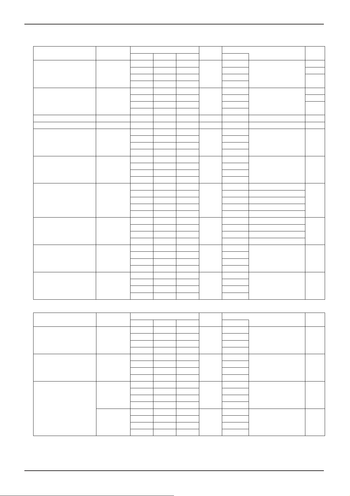
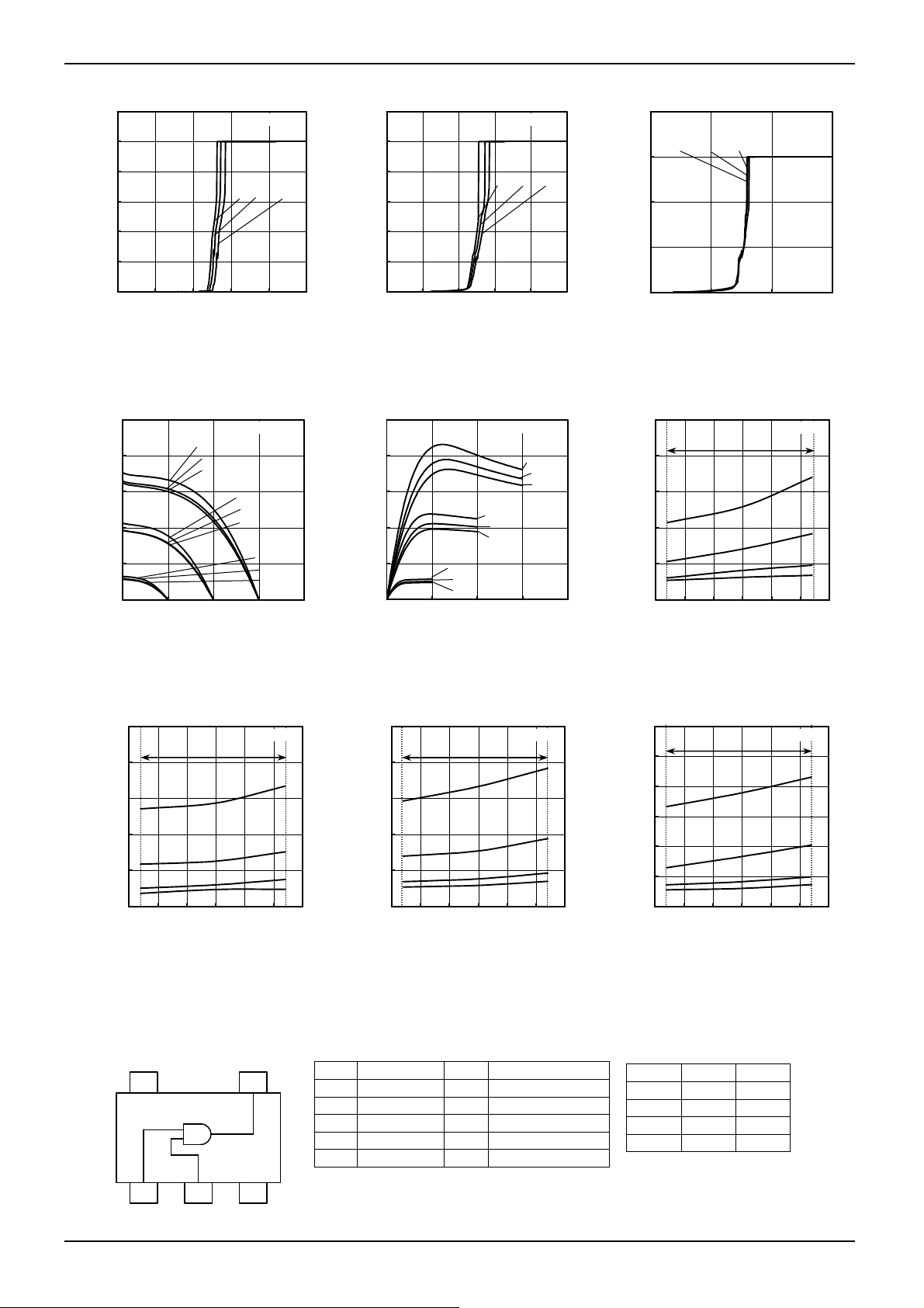
●Electrical Characteristics Curves(BU4S01G2)
6
5
[BU4S10G2] [BU4S10G2] [BU4S01G2]
12
10
4
3
2
Output Voltage [V]
1
0
012345
Output voltage-Input voltage characteristics
50
40
30
20
10
Output Source Current [mA]
0
0 5 10 15 20
Output source current-voltage characteristics
85[℃] 25[℃] -40[℃]
Inpu t Voltage [V]
Fig.1
(VDD=5[V] / VSS=0[V])
VDD=15[V]
-40[℃]
25[℃]
85[℃]
Output Voltage [V]
[BU4S10G2] [BU4S10G2]
VDD=10[V]
-40[℃]
25[℃]
85[℃]
VDD=5[V]
-40[℃]
25[℃]
85[℃]
Fig.4
8
6
4
Output Voltage [V]
2
0
0246810
Output voltage-Input voltage characteristics
(VDD=10[V] / VSS=0[V])
50
40
30
20
Output Sink Current [mA]
10
0
VDD=15[V]
-40[℃]
25[℃]
85[℃]
0 5 10 15 20
Output Voltage [V]
Output sink current-voltage characteristics
250
200
150
Operating Tempretrue Range
[BU4S10G2]
VDD=3[V]
250
200
150
Operating Tempretrue Range
100
Output Fall Time[ns]
VDD=5[V]
50
0
-50 -25 0 25 50 75 100
VDD=10[V]
VDD=16[V]
Ambient Temperature [℃]
Fig.7
Output falling time tTHL
100
50
Propagation Delay Time[ns]
0
-50 -25 0 25 50 75 100
Ambient Temperature [℃]
Propagation delay time tPLH
●Pinout Diagram ・Pin Description・Input / Output Table
VDD Y
54
PIN PIN NAME I/O PIN FUNCTION
1 A I Input
2 B I Input
3 VSS - Power supply(-)
123
ABVSS
4 Y O Output
5 VDD - Power supply(+)
85[℃] 25[℃] -40[℃]
Input Voltage [V]
Fig.2
VDD=10[V]
-40[℃]
25[℃]
-40[℃]
25[℃]
85[℃]
85[℃]
VDD=5[V]
Fig.5
[BU4S10G2]
VDD=3 [V]
VDD=5 [V]
VDD=10[V]
VDD=16[V]
Fig.8
20
15
85[℃] 25[℃] -40[℃]
10
Output Voltage [V]
5
0
0 5 10 15
Input Voltage [V]
Fig.3
Output voltage-Input voltage characteristics
(VDD=15[V] / VSS=0[V])
250
200
150
100
Output Rise Time[ns]
50
0
-50 -25 0 25 50 75 100
Operating Voltage Range
VDD=3[V]
VDD=5[V]
VDD=10[V]
VDD=16[V]
Ambient Temperature [℃]
[BU4S01G2]
Fig.6
Output rising time tTLH
250
Operating Tempretrue Range
200
150
100
50
Propagation Delay Time[ns]
0
-50 -25 0 25 50 75 100
Ambient Temperature [
[BU4S01G2]
VDD=3 [V]
VDD=5 [V]
VDD=10[V]
VDD=16[V]
℃
]
Fig.9
Propagation delay time tPHL
A B Y
L L H
L H L
H L L
H H L
www.rohm.com
© 2009 ROHM Co., Ltd. All rights reserved.
9/16
2009.06 - Rev.A
Page 10
BU4S01G2,BU4S11G2,BU4SU69G2,BU4S71G2,BU4S81G2, BU4S584G2
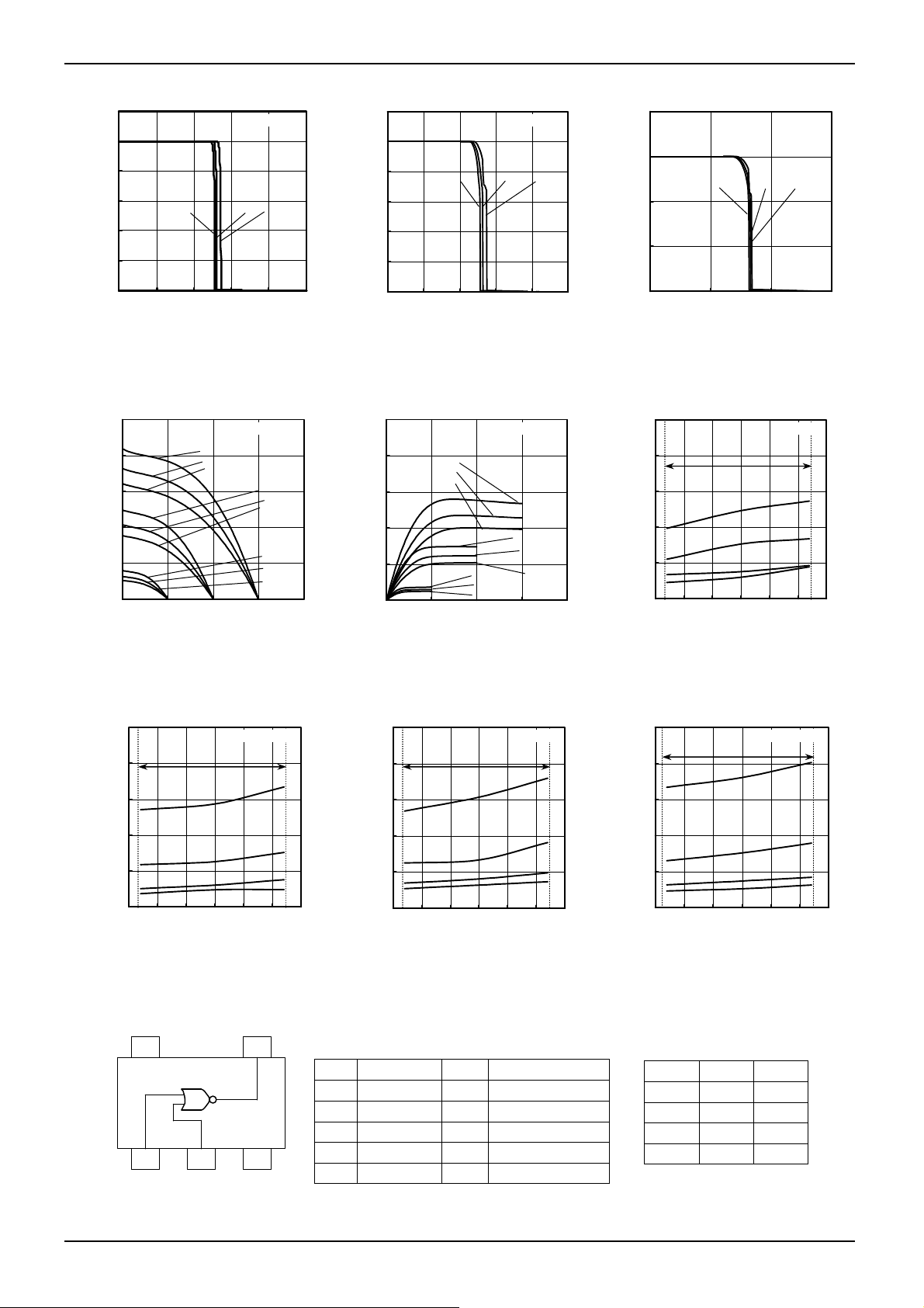
●Electrical Characteristics Curves(BU4S11G2)
6
5
4
3
2
Output Voltage [V]
1
0
012345
Input Voltage [V]
Fig.10
Output voltage-Input voltage characteristics
(VDD=5[V ]/ VSS=0[V])
[BU4S11G2] [BU4S11G2] [BU4S11G2]
85[℃] 25[℃] -40[℃]
12
10
8
6
4
Output Voltage [V]
2
0
0 5 10 15
85[℃] 25[℃] -40[℃]
Input Voltage [V]
Fig.11
Output voltage-Input voltage haracteristics
(VDD=10[V] / VSS=0[V])
20
85[℃] 25[℃] -40[℃]
15
10
Output Voltage [V]
5
0
0 5 10 15
Output voltage-Input voltage characteristics
(VDD=15[V] / VSS=0[V])
50
40
30
20
VDD=15[V]
-40[℃]
25[℃]
85[℃]
10
Output Source Current [mA]
0
0 5 10 15 20
Output Voltage [V]
Fig.13
Output source current-voltage characteristics
[BU4S11G2]
VDD=10[V]
-40[℃]
25[℃]
85[℃]
VDD=5[V]
-40[℃]
25[℃]
85[℃]
50
40
30
20
Output Sink Current [mA]
10
0
0 5 10 15 20
VDD=15[V]
Output Voltage [V]
-40[℃]
25[℃]
85[℃]
-40[℃]
25[℃]
85[℃]
[BU4S11G2]
VDD=10[V]
-40[℃]
25[℃]
85[℃]
VDD=5[V]
Fig.14
Output sink current-voltage characteristics
300
250
200
150
100
Output Rise Time[ns]
50
0
-50 -25 0 25 50 75 100
300
250
200
150
100
Output Fall Time[ns]
50
VDD=3[V]
VDD=5[V]
[BU4S11G2]
]
℃
Operating Temperature Range
VDD=10[V]
0
-50 -25 0 25 50 75 100
VDD=16[V]
Ambient Temperature [
Fig.16
Output falling time tTHL
300
250
200
150
100
Propagation Delay Time[ns]
50
0
Operating Temperature Range
VDD=3[V]
VDD=5[V]
VDD=10[V]
VDD=16[V]
-50 -25 0 25 50 75 100
Ambient Temperature [
Fig.17
Propagation delay time tPLH
[BU4S11G2]
]
℃
300
250
200
150
100
Propagation Delay Time[ns]
50
0
-50 -25 0 25 50 75 100
Propagation delay time tPHL
●Pinout Diagram ・Pin Description・Input / Output Table
VDD Y
54
PIN PIN NAME I/O PIN FUNCTION
1 A I Input
2 B I Input
3 VSS - Power supply(-)
123
ABVSS
4 Y O Output
5 VDD - Power supply(+)
A B Y
L L H
L H H
H L H
H H L
Technical Note
Input Voltage [V]
Fig.12
[BU4S11G2]
Operating Voltage Range
VDD=3[V]
VDD=5[V]
VDD=10[V]
VDD=16[V]
Ambient Temperature [
Fig.15
Output rising time tTLH
Operating Temperature Range
VDD=3[V]
VDD=5[V]
VDD=10[V]
VDD=16[V]
Ambient Temperature [
Fig.18
]
℃
[BU4S11G2]
]
℃
www.rohm.com
© 2009 ROHM Co., Ltd. All rights reserved.
10/16
2009.06 - Rev.A
Page 11

BU4S01G2,BU4S11G2,BU4SU69G2,BU4S71G2,BU4S81G2, BU4S584G2
Technical Note
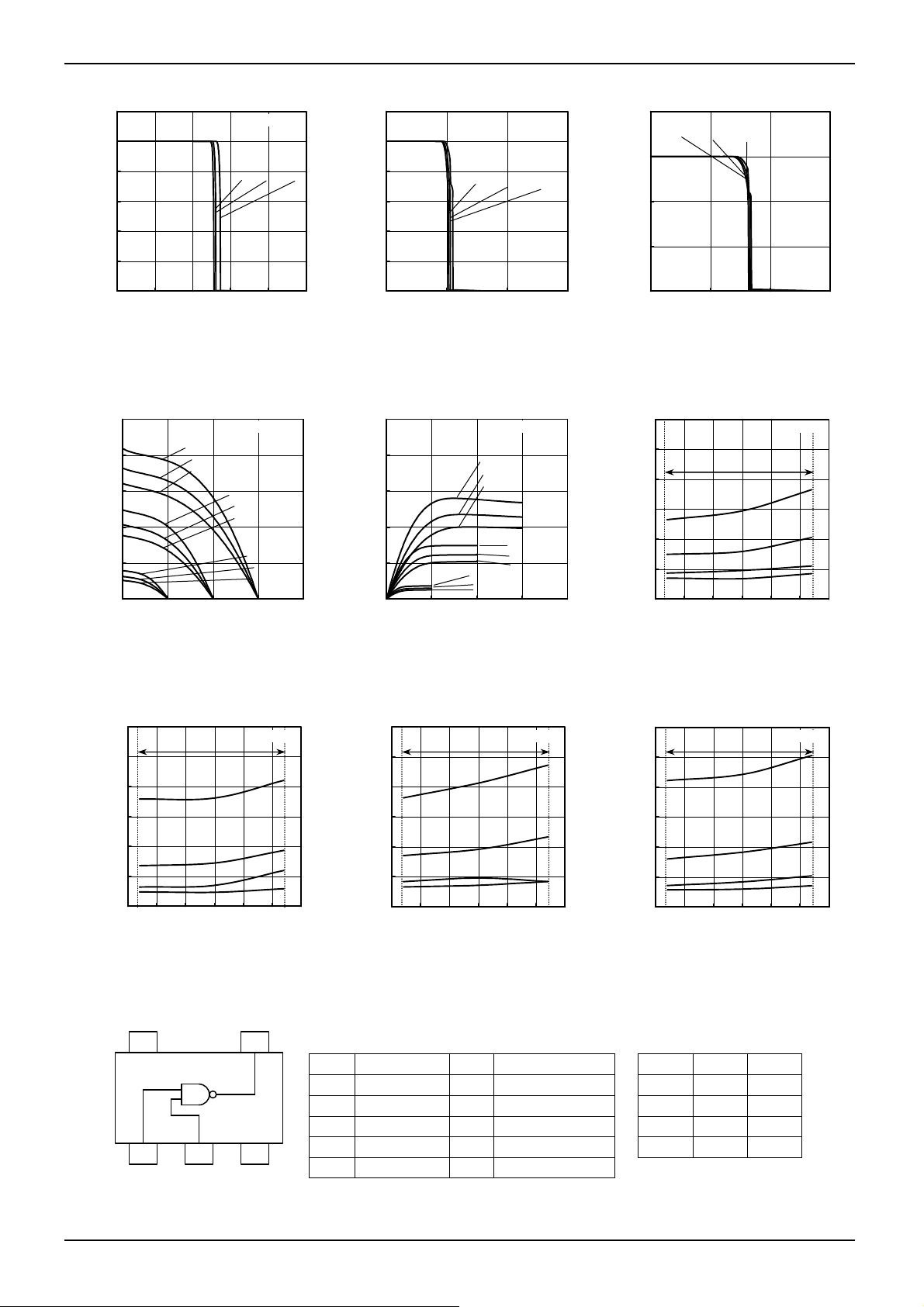
●Electrical Charasteristics Curves (BU4SU69G2)
6
5
4
3
2
Output Voltage [V]
1
0
012345
Output voltage-Input voltage characteristics
Input Voltage [V]
Fig.19
(VDD=5[V] / VSS=0[V])
[BU4S69G2] [BU4S69G2] [BU4S69G2]
85[℃] 25[℃] -40[℃]
12
10
8
6
4
Output Voltage [V]
2
0
0246810
Output voltage-Input voltagecharacteristics
(VDD=10[V] / VSS=0[V])
50
40
30
VDD=15[V]
20
10
Output Source Current [mA]
0
0 5 10 15 20
Output Voltage [V]
Fig.22
Output source current-voltage characteristics
[BU4S69G2] [BU4S69G2]
-40[℃]
25[℃]
85[℃]
VDD=10[V]
-40[℃]
25[℃]
85[℃]
VDD=5[V]
-40[℃]
25[℃]
85[℃]
50
40
30
20
Output Sink Current [mA]
10
0
0 5 10 15 20
Output sink current-voltage characteristics
200
150
[BU4S69G2] [BU4S69G2]
VDD=3[V]
200
150
100
VDD=5[V]
100
Output Fall Time[ns]
50
Operating Temperature Range
0
-50 -25 0 25 50 75 100
Ambient Temperature [
Fig.25
Output falling time tTHL
VDD=10[V]
VDD=16[V]
]
℃
50
Propagation Delay Time[ns]
0
-50 -25 0 25 50 75 100
Propagation delay time tPLH
●Pinout Diagram・Pin Description・Input / Output Table
VDD Y
5 4
1 2 3
NC A VSS
PIN PIN NAME I/O PIN FUNCTION
1 NC - NC
2 A I Input
3 VSS - Power supply(-)
4 Y O Output
5 VDD - Power supply(+)
85[℃] 25[℃] -40[℃]
Input Voltage [V]
Fig.20
VDD=10[V]
-40[℃]
25[℃]
85[℃]
VDD=5[V]
-40[℃]
25[℃]
85[℃]
Output Voltage [V]
Fig.23
Operating Temperature Range
VDD=3[V]
VDD=5[V]
VDD=10[V]
VDD=16[V]
Ambient Temperature [
Fig.26
VDD=15[V]
-40[℃]
]
℃
25[℃]
85[℃]
20
15
10
Output Voltage [V]
5
0
0 5 10 15
85[℃] 25[℃] -40[℃]
Input Voltage [V]
Fig.21
Output voltage-Input voltage characteristics
(VDD=15[V] / VSS=0[V])
200
Operating Temperature Range
150
100
Output Rise Time[ns]
50
0
-50 -25 0 25 50 75 100
VDD=3[V]
VDD=5[V]
VDD=10[V]
VDD=16[V]
Ambient Temperature [
[BU4S69G2]
]
℃
Fig.24
Output rising time tTLH
250
Operating Temperature Range
VDD=3[V]
VDD=5[V]
VDD=10[V]
VDD=16[V]
-50-250 255075100
Ambient Temperature [
Propagation Delay Time[ns]
200
150
100
50
0
[BU4S69G2]
]
℃
Fig.27
Propagation delay time tPHL
A Y
L H
H L
www.rohm.com
© 2009 ROHM Co., Ltd. All rights reserved.
11/16
2009.06 - Rev.A
Page 12
BU4S01G2,BU4S11G2,BU4SU69G2,BU4S71G2,BU4S81G2, BU4S584G2
Technical Note
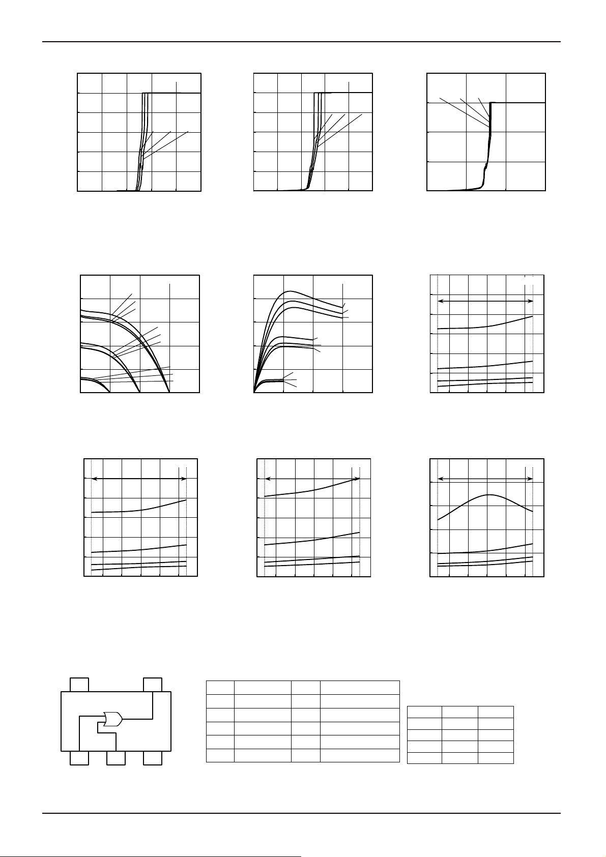
●Electrical Charasteristics Curves (BU4S71G2)
6
5
[BU4S71G2] [BU4S71G2] [BU4S71G2]
12
10
4
3
2
Output Voltage [V]
1
0
012345
Input Voltage [V]
Output voltage-Input voltage characteristics
(VDD=5[V]/ VSS=0[V])
85[℃] 25[℃] -40[℃]
Fig.28
8
6
4
Output Voltage [V]
2
0
0246810
Output voltage-Input voltage characteristics
(VDD=10[V] / VSS=0[V])
50
40
30
20
VDD=15[V]
-40[℃]
10
Output Source Current [mA]
0
0 5 10 15 20
Output Voltage [V]
Fig.31
Output source current-voltage characteristics
300
Operating Temperature Range
VDD=10[V]
0
-50 -25 0 25 50 75 100
VDD=16[V]
Ambient Temperature [
Output Fall Time[ns]
250
200
150
100
50
Fig.34
falling time tTHL
[BU4S71G2] [BU4S71G2]
25[℃]
85[℃]
VDD=10[V]
-40[℃]
25[℃]
85[℃]
VDD=5[V]
-40[℃]
25[℃]
85[℃]
[BU4S71G2]
VDD=3[V]
VDD=5[V]
]
℃
50
40
30
20
Output Sink Current [mA]
10
0
0 5 10 15 20
Output sink current-voltage characteristics
300
Operating Temperature Range
-50 -25 0 25 50 75 100
Ambient Temperature [
Propagation Delay Time[ns]
250
200
150
100
50
0
Propagation delay time tPLH
●Pinout Diagram・Pin Description・Input / Output Table
VDD Y
54
123
ABVSS
PIN PIN NAME I/O PIN FUNCTION
1 A I Input
2 B I Input
3 VSS - Power supply(-)
4 Y O Output
5 VDD - Power supply(+)
85[℃] 25[℃] -40[℃]
Input Voltage [V]
Fig.29
VDD=10[V]
-40[℃]
25[℃]
85[℃]
VDD=5[V]
-40[℃]
25[℃]
85[℃]
Output Voltage [V]
Fig.32
VDD=3[V]
VDD=5[V]
VDD=10[V]
VDD=16[V]
Fig.35
VDD=15[V]
-40[℃]
25[℃]
85[℃]
[BU4S71G2]
]
℃
20
85[℃] 25[℃] -40[℃]
15
10
Output Voltage [V]
5
0
0 5 10 15
Input Voltage [V]
Fig.30
Output voltage-Input voltage characteristics
(VDD=15[V] / VSS=0[V])
300
250
200
150
100
Output Rise Time [ns]
50
0
Operating Temperature Range
VDD=10[V]
VDD=16[V]
-50 -25 0 25 50 75 100
Ambient Temperature[
VDD=3[V]
VDD=5[V]
[BU4S71G2]
]
℃
Fig.33
Rising time tTLH
250
Operating Temperature Range
-50 -25 0 25 50 75 100
Ambient Temperature [
Propagation Delay Time[ns]
200
150
100
50
0
VDD=3[V]
VDD=5[V]
VDD=10[V]
VDD=16[V]
[BU4S71G2]
]
℃
Fig.36
Propagation delay time tPHL
A B Y
L L L
L H H
H L H
H H H
www.rohm.com
© 2009 ROHM Co., Ltd. All rights reserved.
12/16
2009.06 - Rev.A
Page 13
BU4S01G2,BU4S11G2,BU4SU69G2,BU4S71G2,BU4S81G2, BU4S584G2
●Electrical Charasteristics Curves(BU4S81G2)
6
5
[BU4S81G2] [BU4S81G2]
4
3
2
Output Voltage [V]
1
0
012345
Input Voltage [V]
Fig.37
Output voltage-Iput voltage characteristics
(VDD=5[V] / VSS=0[V])
85[℃] 25[℃] -40[℃]
12
10
8
6
4
Output Voltage [V]
2
0
0246810
Input Voltage [V]
85[℃] 25[℃] -40[℃]
Fig.38
Output voltae-Input voltage characteristics
(VDD=10[V] / VSS=0[V])
20
85[℃] 25[℃] -40[℃]
15
10
Output Voltage [V]
5
0
0 5 10 15
Output voltage-Input voltage characteristics
(VDD=15[V] / VSS=0[V])
50
40
30
20
VDD=15[V]
-40[℃]
25[℃]
85[℃]
10
Output Source Current [mA]
0
0 5 10 15 20
Output Voltage [V]
Fig.40
Output source current-voltage characteristics
[BU4S81G2]
VDD=10[V]
-40[℃]
25[℃]
85[℃]
VDD=5[V]
-40[℃]
25[℃]
85[℃]
50
40
30
20
Output Sink Current [mA]
10
0
0 5 10 15 20
VDD=5[V]
-40[℃]
25[℃]
85[℃]
Output Voltage [V]
VDD=10[V]
-40[℃]
25[℃]
85[℃]
[BU4S81G2]
VDD=15[V]
-40[℃]
25[℃]
85[℃]
Fig.41
Output sink current-voltage characteristics
250
200
150
100
Output Rise Time[ns]
50
0
-50 -25 0 25 50 75 100
Technical Note
[BU4S81G2]
Input Voltage [V]
Fig.39
[BU4S81G2]
Operating Temperature Range
VDD=3[V]
VDD=5[V]
VDD=10[V]
VDD=16[V]
Ambient Temperature [
Fig.42
Output rising time tTLH
]
℃
250
200
150
100
Output Fall Time[ns]
50
0
Operating Temperature Range
-50 -25 0 25 50 75 100
Ambient Temperature [
Fig.43
Output falling time tTHL
VDD=3[V]
VDD=5[V]
VDD=10[V]
VDD=16[V]
[BU4S81G2]
]
℃
250
Operating Temperature Range
-50 -25 0 25 50 75 100
Ambient Temperature [
Propagation Delay Time[ns]
200
150
100
50
0
Propagation delay time tPLH
●Pinout Diagram・Pin Description・Input / Output Table
VDD Y
54
PIN PIN NAME I/O PIN FUNCTION
1 NC - Input
2 A I Input
3 VSS - Power supply(-)
4 Y O Output
5 VDD - Power supply(+)
123
ABVSS
VDD=3[V]
VDD=5[V]
VDD=10[V]
VDD=16[V]
Fig.44
[BU4S81G2]
]
℃
300
Operating Temperature Range
VDD=3[V]
VDD=5[V]
VDD=10[V]
VDD=16[V]
-50 -25 0 25 50 75 100
Ambient Temperature [
Propagation Delay Time[ns]
250
200
150
100
50
0
Fig.45
Propagation delay time tPHL
A B Y
L L L
L H L
H L L
H H H
[BU4S81G2]
]
℃
www.rohm.com
© 2009 ROHM Co., Ltd. All rights reserved.
13/16
2009.06 - Rev.A
Page 14

[V]
]
[℃]
BU4S01G2,BU4S11G2,BU4SU69G2,BU4S71G2,BU4S81G2, BU4S584G2
Technical Note
●Electrical Charasteristics Curves(BU4S584G2)
6
5
[BU4S584G2] [BU4S584G2]
12
10
4
3
2
Output Voltage [V]
1
0
012345
Input Voltage [V]
Fig.46
Output voltage-Input voltage characteristics
(VDD=5[V] / VSS=0[V])
50
40
30
20
Output Source Current [mA]
10
0
0 5 10 15 20
VDD=15[V]
Output Voltage [V]
Output source current-voltage characteristics
250
200
150
100
Output Fall Time[ns]
50
Operating Temperature Range
VDD=3[V]
VDD=5[V]
VDD=10[V]
VDD=16[V]
0
-50 -25 0 25 50 75 100
Ambient Temperature [
Output falling time tTHL
-40
25[℃]
85[℃]
Fig.49
Fig.52
85[℃] 25[℃] -40[℃]
[BU4S584G2] [BU4S584G2]
VDD=10[V]
-40[℃]
25[℃]
85[℃]
VDD=5[V]
-40[℃]
25[℃]
85[℃]
[BU4S584G2]
]
℃
8
6
4
Output Voltage [V]
2
0
0246810
Output voltage-Input voltage characteristics
(VDD=10[V] / VSS=0[V])
50
40
30
20
Output Sink Current [mA]
10
0
0 5 10 15 20
Output sink current-voltage characteristics
250
Operating Temperature Range Operating Temperature Range
-50 -25 0 25 50 75 100
Ambient Temperature [
Propagation Delay Time[ns]
200
150
100
50
0
Propagation delay time tPLH
●Pinout Diagram・Pin Description・Input / Output Table
VDD Y
5 4
1 2 3
NC A VSS
PIN PIN NAME I/O PIN FUNCTION
1 NC - NC
2 A I Input
3 VSS - Power supply(-)
4 Y O Output
5 VDD - Power supply(+)
85[℃] 25[℃] -40[℃]
Input Voltage [V]
Fig.47
VDD=10[V]
-40[℃]
25[℃]
85[℃]
VDD=5[V]
-40[℃]
25[℃]
85[℃]
Output Voltage [V]
Fig.50
VDD=3[V]
VDD=5[V]
VDD=10[V]
VDD=16[V]
Fig.53
VDD=15[V]
-40[℃]
25[℃]
85[℃]
[BU4S584G2]
]
℃
20
15
10
Output Voltage [V]
5
0
0 5 10 15
Input Voltage [V]
[BU4S584G2]
85[℃] 25[℃] -40[℃]
Fig.48
Output voltage-Input voltage characteristics
(VDD=15
250
200
150
100
Output Rise Time[ns]
50
0
-50 -25 0 25 50 75 100
/ VSS=0[V
VDD=3[V]
VDD=5[V]
VDD=10[V]
VDD=16[V]
Ambient Temperature [
)
[BU4S584G2]
]
℃
Fig.51
Output rising time tTLH
300
250
200
150
100
Output Rise Time[ns]
50
0
-50 -25 0 25 50 75 100
Ambient Temperature [
[BU4S584G2]
VDD=3[V]
VDD=5[V]
VDD=10[V]
VDD=16[V]
℃
]
Fig.54
Propagation delay time tPHL
A Y
L H
H L
www.rohm.com
© 2009 ROHM Co., Ltd. All rights reserved.
14/16
2009.06 - Rev.A
Page 15

BU4S01G2,BU4S11G2,BU4SU69G2,BU4S71G2,BU4S81G2, BU4S584G2
●Notes for use
1. Absolute Maximum ratings
An excess in the absolute maximum ratings, such as supply voltage, temperature range of oper ating conditions, etc., can
break down the devices, thus making impossible to identify breaking mode, such as short circuit or an open circuit. If any
over rated values will expect to exceed the absolute maximum ratings, consider adding circuit prot ection devices, such as
fuses.
2. Connecting the power supply connector backward
Connecting of the power supply in reverse polarity can damage IC. Take precautions when connecting the power supply
lines. An external direction diode can be added.
3. Power supply lines
Design PCB layout pattern to provide low impedance GND and supply lines. To obtain a low noise ground and supply line,
separate the ground section and supply lines of the digital and analog blocks. Furthermore, for all power supply terminals to
ICs, connect a capacitor between the power supply and the GND terminal. When applying electrol ytic capacitors in the
circuit, not that capacitance characteristic values are reduced at low temperatures.
4. GND voltage
The potential of GND pin must be minimum potential in all operating conditions.
5. Thermal design
Use a thermal design that allows for a sufficient margin in light of the power dissipation (Pd) in actual operating conditions.
6. Inter-pin shorts and mounting errors
Use caution when positioning the IC for mounting on printed circuit boards. The IC may be damaged if there is any
connection error or if pins are shorted together.
7. Actions in strong electromagnetic field
Use caution when using the IC in the presence of a strong electromagnetic field as doing so may cause the IC to
malfunction.
8. Testing on application boards
When testing the IC on an application board, connecting a capacitor to a pin with low impedance subjects the IC to stress.
Always discharge capacitors after each process or step. Always turn the IC's power supply off before connecting it to or
removing it from a jig or fixture during the inspection process. Ground the IC during assembly steps as an antistatic measure.
Use similar precaution when transporting or storing the IC.
9. Ground Wiring Pattern
When using both small signal and large current GND patterns, it is recommended to isolate the two ground patterns, placing
a signal ground point at the ground potential of application so that the pattern wiring resistance and voltage variations
caused by large currents do not cause variations in the small signal ground voltage. Be careful not to change the GND wiring
pattern of any external components, either.
10. Unused input terminals
Connect all unused input terminals to VDD or VSS in order to prevent excessive current or oscillation.
Insertion of a resistor (100kΩ approx.) is also recommended.
Technical Note
www.rohm.com
© 2009 ROHM Co., Ltd. All rights reserved.
15/16
2009.06 - Rev.A
Page 16

BU4S01G2,BU4S11G2,BU4SU69G2,BU4S71G2,BU4S81G2, BU4S584G2
●Ordering part number
B U 4 S 0 1 G 2 - T R
Technical Note
Part No. Part No.
Package
4S01 , 4S11
4SU69 , 4S71
4S81 , 4S584
SSOP5
<Tape and Reel information>
Quantity
Direction
of feed
2.8±0.2
1.25Max.
1.1±0.05
°
+0.05
−0.04
4
0.13
+
6
°
°
−4
0.2Min.
+0.05
−0.03
2.9±0.2
5
4
+0.2
−0.1
1.6
12
3
0.95
0.05±0.05
0.42
0.1
(Unit : mm)
Packaging and forming specification
G2: SSOP5
TR: Embossed tape and reel
Embossed carrier tapeTape
3000pcs
TR
The direction is the 1pin of product is at the upper right when you hold
()
reel on the left hand and you pull out the tape on the right hand
1pin
Direction of feed
Reel
Order quantity needs to be multiple of the minimum quantity.
∗
www.rohm.com
© 2009 ROHM Co., Ltd. All rights reserved.
16/16
2009.06 - Rev.A
Page 17

Notes
No copying or reproduction of this document, in part or in whole, is permitted without the
consent of ROHM Co.,Ltd.
The content specied herein is subject to change for improvement without notice.
The content specied herein is for the purpose of introducing ROHM's products (hereinafter
"Products"). If you wish to use any such Product, please be sure to refer to the specications,
which can be obtained from ROHM upon request.
Examples of application circuits, circuit constants and any other information contained herein
illustrate the standard usage and operations of the Products. The peripheral conditions must
be taken into account when designing circuits for mass production.
Great care was taken in ensuring the accuracy of the information specied in this document.
However, should you incur any damage arising from any inaccuracy or misprint of such
information, ROHM shall bear no responsibility for such damage.
The technical information specied herein is intended only to show the typical functions of and
examples of application circuits for the Products. ROHM does not grant you, explicitly or
implicitly, any license to use or exercise intellectual property or other rights held by ROHM and
other par ties. ROHM shall bear no responsibility whatsoever for any dispute arising from the
use of such technical information.
Notice
The Products specied in this document are intended to be used with general-use electronic
equipment or devices (such as audio visual equipment, ofce-automation equipment, communication devices, electronic appliances and amusement devices).
The Products specied in this document are not designed to be radiation tolerant.
While ROHM always makes efforts to enhance the quality and reliability of its Products, a
Product may fail or malfunction for a variety of reasons.
Please be sure to implement in your equipment using the Products safety measures to guard
against the possibility of physical injury, re or any other damage caused in the event of the
failure of any Product, such as derating, redundancy, re control and fail-safe designs. ROHM
shall bear no responsibility whatsoever for your use of any Product outside of the prescribed
scope or not in accordance with the instruction manual.
The Products are not designed or manufactured to be used with any equipment, device or
system which requires an extremely high level of reliability the failure or malfunction of which
may result in a direct threat to human life or create a risk of human injury (such as a medical
instrument, transportation equipment, aerospace machinery, nuclear-reactor controller,
fuel-controller or other safety device). ROHM shall bear no responsibility in any way for use of
any of the Products for the above special purposes. If a Product is intended to be used for any
such special purpose, please contact a ROHM sales representative before purchasing.
If you intend to export or ship overseas any Product or technology specied herein that may
be controlled under the Foreign Exchange and the Foreign Trade Law, you will be required to
obtain a license or permit under the Law.
www.rohm.com
© 2009 ROHM Co., Ltd. All rights reserved.
Thank you for your accessing to ROHM product informations.
More detail product informations and catalogs are available, please contact us.
ROHM Customer Support System
http://www.rohm.com/contact/
R0039
A
 Loading...