

1
General-purpose CMOS Logic IC Series (BU4S,BU4000B Series)
Single Gate CMOS Logic ICs
<Analog Switch>
BU4S66G2
●Description
The BU4S66G2 is a 1ch analog switch IC encapsulated in an SSOP5 package, and can replace 1 circuit of the
general-purpose CMOS two-way analog switch BU4066B IC.
●Features
1) Low power consumption
2) Surface mount package (SSOP5)
3) Broad operating supply voltage range: 3V-16V
4) L-TTL2 and LS-TTL1 inputs can be driven directly
5) Function compatible with BU4066BC series (1ch).
6) Excellent linearity
●Applications
Can be used as a digital/analog switch, ON/OFF switch, or changeover switch in a high speed line, with no deterioratio n of
the analog signals. Connection to a low impedance circuit is possible, due to the low ON resistance.
●Lineup
Single gate
analog switch
circuit
Switch
BU4S66G2 (Single analog switch)
No. 09050JAT02
www.rohm.com
© 2009 ROHM Co., Ltd. All rights reserved.
1/7
2009.06 - Rev.A
BU4S66G2
A
●Absolute Maximum Ratings
Parameter Symbol Limit Unit
Power Supply Voltage VDD -0.3 to 18 V
Supply Current Iin ±10 mA
Operating Temperature Topr -40 to 85 ℃
Storage Temperature Tstg -55 to 150 ℃
Input Voltage VIN -0.3 to VDD+0.3 V
Maximum Junction Temperature Tjmax 150 ℃
●Recommended Operating Conditions
Parameter
Symbol Limit Unit
Operating Power Supply VDD 3 to 16 V
Input Voltage VIN 0 to VDD V
●Thermal Derating Curve
1400
1200
1000
800
600
400
Power Dissipation Pd [mW]
200
0
660[mW] BU4S66G2 (*1)
85
℃
25 50 75 100 125 150
mbient Temperature Ta [℃]
(*1) Unit
5.3 mW/℃
Reduced per 1C at Ta>25℃. Power Dissipation measured when sample mounted on
175
a 70mm×70mm×1.6mm FR4 glass-epoxy PCB (copper area less than 3%)
●Input / Output Equivalent Circuits
VDD
VDD VDD
GND
<Analog Switch Input/Output>
GND
<Control Input>
Technical Note
GND
www.rohm.com
© 2009 ROHM Co., Ltd. All rights reserved.
2/7
2009.06 - Rev.A
BU4S66G2
Technical Note
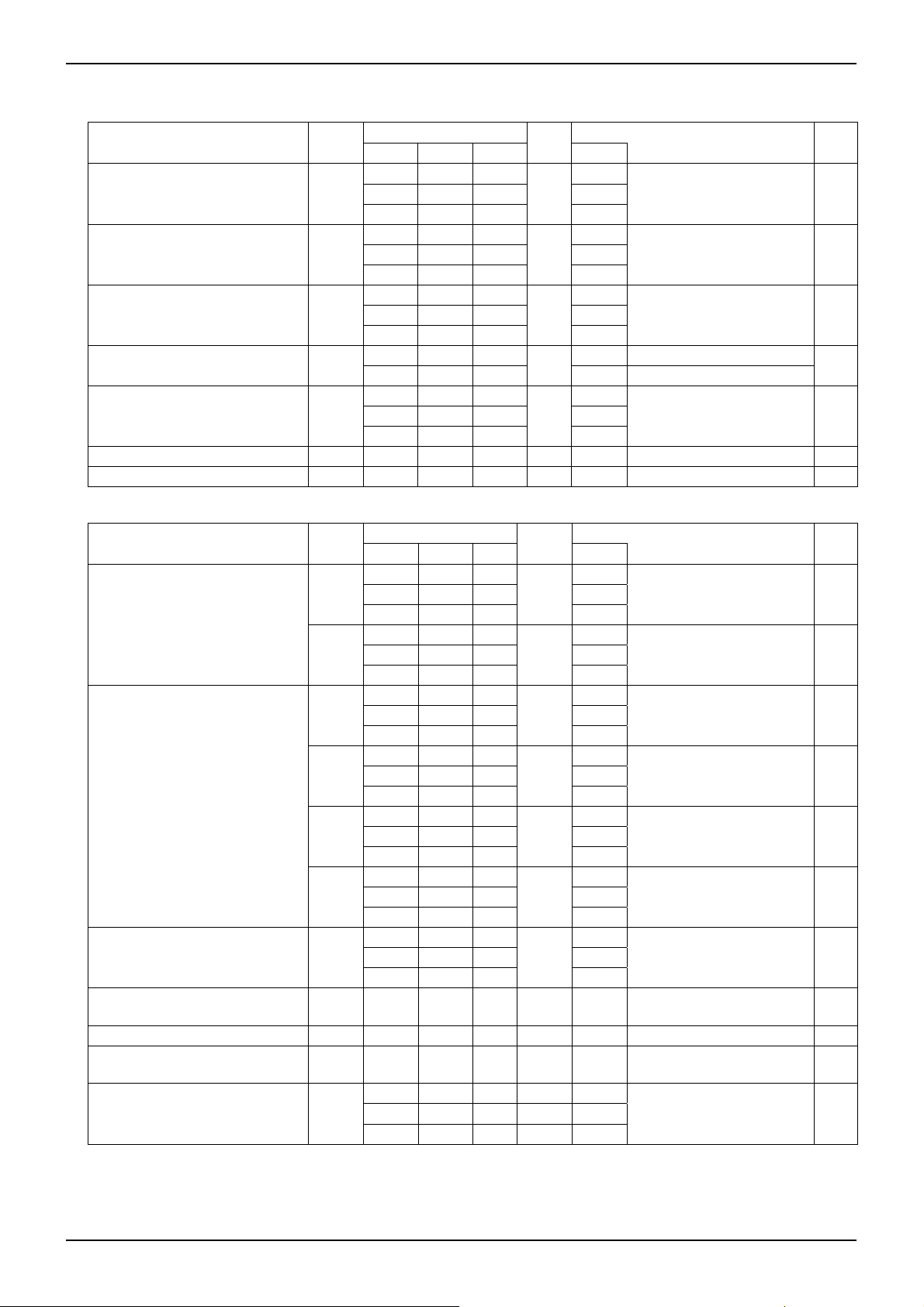
●Electrical Characteristics (BU4S66G2)
DC Characteristics (Unless otherwise noted : VSS=0[V],Ta=25[℃])
Parameter Symbol
Control “H”input voltage VIH
Control “L”input voltage VIL
ON resistance RON
Channel-OFF
Leakage current
LOFF
Static supply current IDD
Limits
Min Typ Max VDD[V]
Unit
3.5 - -
V
11.0 - - 15
- - 1.5
V
- - 4.0 15
- 290 950
Ω
- 85 160 15
- - 0.3
- - -0.3 15 VIN=0[V],VOUT=15[V]
μA
- - 1.0
μA
5
Current between in and
Condition Fig.No
out=10[μA]
5
Current between in and out
=10[μA]
5
0≦VIN≦VDD
RL=10[kΩ]
15 VIN=15[V],VOUT=0[V]
5
VIN=VDD or GND - - - 2.0 10
- - 4.0 15
Input capacitance(control input) CC - 8 - pF - f=1[MHz] -
Input capacitance(switch input) CS - 10 - pF - f=1[MHz] -
Switching Characteristics (Unless otherwise noted : VSS=0[V],Ta=25[℃],CL=50[pF])
Parameter Symbol
Propagation delay time
(I/O→O/I)
Propagation delay time
(CONTROL→O/I)
Maximum control frequency
Maximum propagation frequency
tPLH
tPHL
tPHZ
tPLZ
tPZH
tPZL
fmax
(C)
Fmax
(I-O)
Limits
Min Typ Max VDD[V]
Unit
- 15 -
- 8 - 10
ns
- 5 - 15
- 15 -
- 8 - 10
ns
- 5 - 15
- 100 -
- 70 - 10
ns
- 65 - 15
- 100 -
- 70 - 10
ns
- 65 - 15
- 80 -
- 35 - 10
ns
- 25 - 15
- 80 -
- 35 - 10
ns
- 25 - 15
- 10 -
- 12 - 10
MHz
- 12 - 15
- 30 - MHz 5
*1
5
RL=10[kΩ]
CL=50[pF]
5
RL=10[kΩ]
CL=50[pF]
5
RL=10[kΩ]
CL=50pF
5
RL=10[kΩ]
CL=50[pF]
5
RL=10[kΩ]
CL=50[pF]
5
RL=10[kΩ]
CL=50[pF]
5
RL=1[kΩ]
CL=50[pF]
VSS=-5[V],RL=1[kΩ]
CL=50[pF]
Condition Fig.No
Feedthrough attenuation FT*2 - 600 - kHz 5 VSS=-5[V],RL=1[kΩ] -
Sine wave distortion (1[kHz]) THD*3 - 0.05 - % 5
- 200 - mV 5
Cross talk (CONTROL→O/I) CTc
- 400 - mV 10
- 600 - mV 15
*1 Frequency where 20log(VOUT/VIN)=3[dB]
*2 Frequency where 20log(VOUT/VIN)=50[dB]
*1 *2 *3 Must be sine wave of VIN±2.5[Vp-p].
VSS=-5[V],RL=10[kΩ]
CL=50[pF]
RIN=1[kΩ]
ROUT=10[kΩ]
CL=15[pF]
- 7.0 - - 10
- - - 3.0 10
1 - 120 250 10
-
2
3
4
5
6
7
-
-
-
-
www.rohm.com
© 2009 ROHM Co., Ltd. All rights reserved.
3/7
2009.06 - Rev.A

BU4S66G2
]
[℃]
[℃]
[℃]
[℃]
[℃]
[℃]
[℃]
[℃]
[
]
A
[
]
Technical Note
●Electrical Characteristics Curves
400
[BU4S66G2]
300
]
Ω
200
On Resistance [
100
Fig.1 Output current-voltage
VDD=5[V]
85
VDD=10[V]
25
-40
0
0 5 10 15
Input Voltage [V]
85
VDD=15[V]
25
-40
200
150
VDD=3[V]
VDD=5[V]
100
50
Propagation Delay Time[ns]
Operating T emp eratur e Range
0
-50 -25 0 25 50 75 100
Ambient Temperature [℃]
[BU4S66G2]
VDD=16[V]
VDD=10[V]
Fig.4 Propagation delay tPHZ
(CONT-OUT)
200
150
VDD=3[V]
[BU4S66G2]
85
25
-40[℃]
200
Operating T emp eratur e Range
150
100
BU4S66G2
VDD=3[V]
VDD=5[V]
50
Propagation Delay Time[ns]
0
-50 -25 0 25 50 75 100
Ambient Temperature [℃]
VDD=10[V]
VDD=16[V]
Fig.2 Propagation delay tPLH
(IN-OUT)
200
150
VDD=3[V]
[BU4S66G2]
200
Operating T emp eratur e Range
150
100
[BU4S66G2]
VDD=3[V]
VDD=5[V]
50
Propagation Delay Time[ns
0
-50 -25 0 25 50 75 100
Ambient Temperature [℃]
Fig.3 Propagation delay tPHL
VDD=10[V]
VDD=16[V]
(IN-OUT)
200
Operating T emp eratur e Range
150
VDD=3[V]
BU4S66G2
VDD=5[V]
100
VDD=16[V]
100
VDD=5[V]
VDD=10[V]
Propagation Delay Time[ns]
50
VDD=10[V]
VDD=16[V]
0
-50 -25 0 25 50 75 100
mbient T emper ature [℃]
Fig.6 Propagation delay tPZH
(CONT-OUT)
50
Propagation Delay Time[ns]
Operating T emp eratur e Range
0
-50 -25 0 25 50 75 100
Ambient Temperature [℃]
Fig.5 Propagation delay tPLZ
(CONT-OUT)
Operating T emp eratur e Range
100
VDD=5[V]
Propagation Delay Time[ns]
50
VDD=10[V]
VDD=16[V]
0
-50 -25 0 25 50 75 100
Ambient Temperature [℃]
Fig.7 Propagation delay tPZL
(CONT-OUT)
www.rohm.com
© 2009 ROHM Co., Ltd. All rights reserved.
4/7
2009.06 - Rev.A

BU4S66G2
Technical Note
●Pinout Diagram・Pin Description・Input / Output Table
Pinout Diagram Input / Output Table
VDD
54
CONT
CONT SW
L OFF
H ON
Pin Description
123
I/O
O/I VSS
●Measurement Circuit
SW2SW1
VDD
SW3
SW4 SW 5 SW6
SW7
A
I/O
VIN
PG
~
RL
Pin No Symbol I/O Function
1 I/O I/O Analog Switch Input / Output
2 O/I I/O Analog Switch Input / Output
3 VSS ― Power supply(-)
4 CONT I Control Input
5 VDD ― Power supply(+)
20[ns] 20[ns]
90%
50%
10%
tpLH
50%
10%
tTLH tTHL
90%
tpHL
RL
SW12 SW13 SW14
O/I
SW15 SW16 SW 17
VDD
CL
Input
入力波形
Output
出力波形
Switching Characteristics
RL CL
入力波形
Input
SW8 SW9 SW10 SW11
A
CONT
VSS
50%
~
VIN
PG
Output
出力波形
tPLZ
10%
tPZL
Propagation delay
●Switching Table
Parameter
Input voltage/current OFF ON OFF OFF OFF OFF OFF ON OFF OFF OFF OFF OFF OFF ON OFF OFF
ON resistance ON OFF ON OFF OFF OFF OFF OFF OFF OFF OFF OFF OFF OFF ON OFF OFF
Channel-OFF
Leakage current
Switching Characteristics
Propagation time
CONT→OUT
Sine wave distortion
Feedthrough attenuation
Control OFF OFF OFF OFF OFF OFF ON OFF OFF OFF ON OFF OFF OFF ON ON OFF
SW 1 SW2 SW 3 SW 4 SW5 SW6 SW7 SW8 SW9 SW
10 SW11
OFF ON OFF OFF OFF OFF OFF OFF ON OFF OFF OFF OFF ON OFF OFF ON
OFF OFF OFF ON OFF OFF OFF OFF ON OFF OFF OFF OFF OFF OFF OFF OFF
ON OFF OFF OFF ON OFF OFF OFF OFF OFF OFF OFF OFF OFF ON ON OFF
tPLZ OFF OFF OFF OFF ON OFF OFF OFF OFF OFF OFF OFF OFF OFF OFF OFF OFF
tPZL OFF ON OFF OFF OFF OFF OFF OFF OFF ON OFF ON ON OFF ON ON OFF
ON OFF OFF OFF OFF ON OFF OFF OFF ON OFF OFF OFF OFF ON ON OFF
OFF OFF OFF OFF OFF ON OFF OFF ON OFF OFF OFF OFF OFF ON ON OFF
SW
12
SW
SW
13
14 SW15 SW16 SW17
50%
50%
www.rohm.com
© 2009 ROHM Co., Ltd. All rights reserved.
5/7
2009.06 - Rev.A

BU4S66G2
●Notes for use
1. Absolute maximum ratings
An excess in the absolute maximum ratings, such as supply voltage, temperature range of operating conditions, etc., can
break down the devices, thus making impossible to identify breaking mode, such as a short circuit or an open circuit. If any
over rated values will expect to exceed the absolute maximum ratings, consider ad ding circuit protection devices, such as
fuses.
2. Connecting the power supply connector backward
Connecting of the power supply in reverse polarity can da mage IC. Take precautions when connecting the power supply
lines. An external direction diode can be added.
3. Power supply lines
Design PCB layout pattern to provide low impedance GND and supply lines. To obtain a low noise ground and supply line,
separate the ground section and supply lines of the digital a nd analog bl ocks. F urthermore, for all p ower supply termina ls
to ICs, connect a capacitor between the power supply and the GND terminal. When applying electrolytic capacitors in the
circuit, not that capacitance characteristic values are reduced at low temperatures.
4. GND voltage
The potential of GND pin must be minimum potential in all operating conditions.
5. Thermal design
Use a thermal design that allows for a sufficient margin in light of the power dissipation (Pd) in actual operating conditions.
6. Inter-pin shorts and mounting errors
Use caution when positioning the IC for mounting on printed circuit boards. The IC may be damaged if there is any
connection error or if pins are shorted together.
7. Actions in strong electromagnetic field
Use caution when using the IC in the presence of a strong electromagnetic field as doing so may cause the IC to
malfunction.
8. Testing on a pplication boards
When testing the IC on an application board, connecting a capacitor to a pin with low impedance subjects the IC to stress.
Always discharge capacitors after each process or step. Always turn the IC's power supply off before conn ecting it to or
removing it from a jig or fixture during the inspection process. Ground the IC during assembly steps as an antistatic
measure. Use similar precaution when transporting or storing the IC.
9. Ground Wiring Pattern
When using both small signal and large current GND patterns, it is recommended to isolate the t wo ground patterns,
placing a single ground point at the ground potential of application so that the pattern wiring resistance and voltage
variations caused by large currents do not cause variations in the small signal ground voltage. Be careful not to change the
GND wiring pattern of any external components, either.
Technical Note
www.rohm.com
© 2009 ROHM Co., Ltd. All rights reserved.
6/7
2009.06 - Rev.A

BU4S66G2
●Ordering part number
B U 4 S 6 6 G 2 - T R
Technical Note
Part No. Part No.
Package
4S66
SSOP5
<Tape and Reel information>
Quantity
Direction
of feed
2.8±0.2
1.25Max.
1.1±0.05
°
+0.05
−0.04
+
6
°
4
°
−4
+0.05
0.13
−0.03
(Unit : mm)
0.2Min.
2.9±0.2
5
4
+0.2
−0.1
1.6
12
3
0.95
0.05±0.05
0.42
0.1
Packaging and forming specification
G2: SSOP5
TR: Embossed tape and reel
Embossed carrier tapeTape
3000pcs
TR
The direction is the 1pin of product is at the upper right when you hold
()
reel on the left hand and you pull out the tape on the right hand
1pin
Direction of feed
Reel
Order quantity needs to be multiple of the minimum quantity.
∗
www.rohm.com
© 2009 ROHM Co., Ltd. All rights reserved.
7/7
2009.06 - Rev.A

Notes
No copying or reproduction of this document, in part or in whole, is permitted without the
consent of ROHM Co.,Ltd.
The content specied herein is subject to change for improvement without notice.
The content specied herein is for the purpose of introducing ROHM's products (hereinafter
"Products"). If you wish to use any such Product, please be sure to refer to the specications,
which can be obtained from ROHM upon request.
Examples of application circuits, circuit constants and any other information contained herein
illustrate the standard usage and operations of the Products. The peripheral conditions must
be taken into account when designing circuits for mass production.
Great care was taken in ensuring the accuracy of the information specied in this document.
However, should you incur any damage arising from any inaccuracy or misprint of such
information, ROHM shall bear no responsibility for such damage.
The technical information specied herein is intended only to show the typical functions of and
examples of application circuits for the Products. ROHM does not grant you, explicitly or
implicitly, any license to use or exercise intellectual property or other rights held by ROHM and
other par ties. ROHM shall bear no responsibility whatsoever for any dispute arising from the
use of such technical information.
Notice
The Products specied in this document are intended to be used with general-use electronic
equipment or devices (such as audio visual equipment, ofce-automation equipment, communication devices, electronic appliances and amusement devices).
The Products specied in this document are not designed to be radiation tolerant.
While ROHM always makes efforts to enhance the quality and reliability of its Products, a
Product may fail or malfunction for a variety of reasons.
Please be sure to implement in your equipment using the Products safety measures to guard
against the possibility of physical injury, re or any other damage caused in the event of the
failure of any Product, such as derating, redundancy, re control and fail-safe designs. ROHM
shall bear no responsibility whatsoever for your use of any Product outside of the prescribed
scope or not in accordance with the instruction manual.
The Products are not designed or manufactured to be used with any equipment, device or
system which requires an extremely high level of reliability the failure or malfunction of which
may result in a direct threat to human life or create a risk of human injury (such as a medical
instrument, transportation equipment, aerospace machiner y, nuclear-reactor controller,
fuel-controller or other safety device). ROHM shall bear no responsibility in any way for use of
any of the Products for the above special purposes. If a Product is intended to be used for any
such special purpose, please contact a ROHM sales representative before purchasing.
If you intend to export or ship overseas any Product or technology specied herein that may
be controlled under the Foreign Exchange and the Foreign Trade Law, you will be required to
obtain a license or permit under the Law.
Thank you for your accessing to ROHM product informations.
More detail product informations and catalogs are available, please contact us.
ROHM Customer Support System
www.rohm.com
© 2009 ROHM Co., Ltd. All rights reserved.
http://www.rohm.com/contact/
R0039
A
 Loading...