

090FS
Serial-in / Parallel-out Driver Series
Serial / Parallel
2-input Drivers
BU2098F, BU2090F, BU2090FS
No.11051EBT04
●Description
Serial-in-parallel-out driver is a open drain output driver. It incorporates a built-in shift register and a latch circuit to turn on a
maximum of 12 LED by a 2-line interface, linked to a microcontroller.
A open drain output provides maximum of 25mA current.
●Features
1) LED can be driven directly. (Output current 25mA)
2) 8/12 Bit parallel output
3) This product can be operated on low voltage.
4) Compatible with I
2
C BUS. (BU2098)
●Use
For AV equipment such as, audio stereo sets, videos and TV sets, PCs, control microcontroller mounted equipment.
●Line up
Parameter BU2098F BU2090F BU2090FS Unit
Output current 25 25 mA
Output line 8 12 lines
Package SOP16 SOP16 SSOP-A16 -
●Thermal derating curve
700
600
500
400
300
200
Power dissipation Pd [mW]
100
0
25 50
85℃
75 100
BU2098F
125 150
175
700
600
BU2
BU2090F
125 150
175
500
400
300
200
Power dissipation Pd [mW]
100
0
25 50
75 100
Ambient temperature Ta [℃]
www.rohm.com
© 2011 ROHM Co., Ltd. All rights reserved.
1/12
2011.12 - Rev.B
BU2098F, BU2090F, BU2090FS
●Electrical characteristics
BU2098F (unless otherwise noted, VDD=5V, Vss=0V, Ta=25℃)
Parameter Symbol Min. Typ. Max. Unit Condition
Input High-level voltage VIH 0.7×VDD - - V
Technical Note
Input Low-level voltage VIL - - 0.3×VDD V
Output Low-level voltage VOL - - 0.4 V IOUT=10mA
Input Low-level current IIL - 2.0 μA VIN=0
Input High-level current IIH - - -2.0 μA VIN=VDD
Output leakage current IOZ - - ±5.0 μA
Static dissipation current IDD - - 2.0 μA
Output=High impedance
OUT=VDD
V
BU2090F/BU2090FS (unless otherwise noted, V
DD=5V, VSS=0V, Ta=25℃)
Parameter Symbol Min. Typ. Max. Unit Condition
Input High-level voltage VIH
Input Low-level voltage VIL
Output Low-level voltage VOL
3.5 - - V V
2.5 - - V VDD=3V
- - 1.5 V V
- - 0.4 V VDD=3V
- - 2.0 V V
- - 1.0 V VDD=3V,IOL=5mA
DD=5V
DD=5V
DD=5V,IOL=20mA
“H” output disable current IOZH - - 10 μA VO=25V
“L” output disable current IOZL - -5.0 μA VO=0V
Static dissipation current IDD
- - 5.0 μA VDD=5V
3.0 μA VDD=3V
●Operating conditions (Ta=25℃, VSS=0V)
Parameter Symbol
BU2098F BU2090F/BU2090FS
Limits
Unit
Power Supply Voltage VDD +2.7 to 5.5 V
Output Voltage Vo 0 to +15 0 to +25 V
●Absolute maximum ratings
BU2098F, BU2090F,BU2090FS
Parameter Symbol
BU2098F BU2090F BU2090FS
Limits
Unit
Power supply voltage VDD -0.5 to +7.0 -0.3 to +7.0V V
Power dissipation1 Pd1 300 *1 300 *1 500 *2
Power dissipation2 Pd2 - 500 *3 650 *4
mW
Operating temperature range Topr -40 to +85 ℃
Storage temperature range Tstg -55 to +125 ℃
Output voltage Vo VSS to +18.0 VSS-0.3 to +25V V
Input voltage VIN -0.5 to VDD+0.5 VSS-0.3 to VDD+0.3V V
Allowable loss of single unit
* Reduced by 3mW/℃ over 25℃. (BU2098F)
1
*
Reduced by 3mW/℃ over 25℃.
2
*
Reduced by 5mW/℃ over 25℃.
3
*
Reduced by 5.0mW for each increase in Ta of 1℃ over 25℃.(When mounted on a board 70mm×70mm×1.6mm Glass-epoxy PCB)
4
*
Reduced by 6.5mW for each increase in Ta of 1℃ over 25℃.(When mounted on a board 70mm×70mm×1.6mm Glass-epoxy PCB)
www.rohm.com
© 2011 ROHM Co., Ltd. All rights reserved.
2/12
2011.12 - Rev.B
BU2098F, BU2090F, BU2090FS
●Pin descriptions
BU2098F
PIN No. Pin Name I/O Function
1 A0 I
3 A2 I
4 Q0
5 Q1
6 Q2
O Open drain output
7 Q3
8 VSS - GND
9 Q4
10 Q5
11 Q6
O Open drain output
12 Q7
13 N.C. - Non connected
14 SCL I
15 SDA I/O
16 VDD -
BU2090F/BU2090FS
PIN No. Pin Name I/O Function
1 VSS - GND
2 DATA I Serial data input
3 CLOCK I
4 Q0
5 Q1
6 Q2
7 Q3
8 Q4
9 Q5
10 Q6
O
11 Q7
12 Q8
13 Q9
14 Q10
15 Q11
16 VDD -
Technical Note
Address input, internally pull-up 2 A1 I
Serial clock input
Serial data input/output
Power supply
Data shift clock input (rising edge trigger)
The shift data is transferred to the output when the input data logic
level is high during the falling transition of the clock pulse.
Parallel data output (Nch Open Drain FET)
Latch data L H
Output FET ON OFF
Power supply
www.rohm.com
© 2011 ROHM Co., Ltd. All rights reserved.
3/12
2011.12 - Rev.B
BU2098F, BU2090F, BU2090FS
A
A
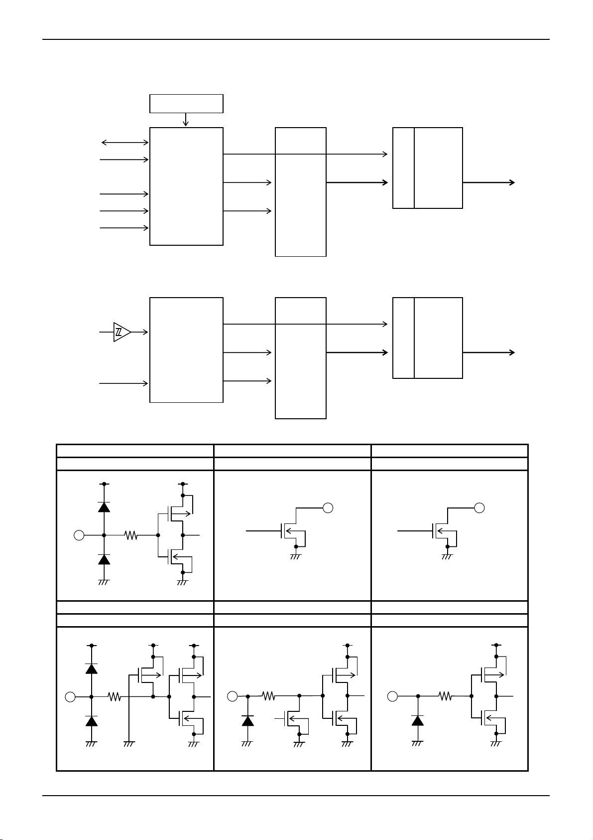
●Block diagram
BU2098F
Power-On Reset
SD
SCL
A0
A1
A2
I2C BUS
Controller
BU2090F/BU2090FS
CLOCK
Controller
DAT
●Interfaces
BU2090F/BU2090FS BU2090F/BU2090FS BU2098F
DATA, CLOCK Q0~Q11 Q0~Q7
V
V
DD
DD
IN
GND (V
)
SS
GND (V
)
SS
BU2098F BU2098F BU2098F
A0~A2 SDA SCL
V
V
DD
VDD
DD
IN
GND (V
)
GND (VSS)
SS
GND (V
SS
Technical Note
Shift
8bit
Register
Shift
12bit
Register
OUT
GND (VSS)
V
DD
IN
GND (V
)
)
GND (VSS)
SS
GND (V
)
SS
L
a
t
c
h
L
a
t
c
h
IN
GND (V
Write
Buffer
Write
Buffer
GND (VSS)
)
SS
Q0~Q11
OUT
V
DD
GND (V
Q0~Q7
)
SS
www.rohm.com
© 2011 ROHM Co., Ltd. All rights reserved.
4/12
2011.12 - Rev.B

BU2098F, BU2090F, BU2090FS
Technical Note
【BU2098F】
●AC characteristics (Unless otherwise noted, VDD=5V, VSS=0V, Ta=25℃)
2
Parameter Symbol
Fast mode I
Min. Max. Min. Max.
C BUS Standard mode I2C BUS
Unit
SCL clock frequency fSCL 0 400 0 100 kHz
Bus free time between start-stop condition tBUS 1.3 - 4.7 - μs
Hold time start condition tHD:STA 0.6 - 4.0 - μs
Low period of the SCL clock tLOW 1.3 - 4.7 - μs
High period of the SCL clock tHIGH 0.6 - 4.0 - μs
Set up time Re-start condition tSU:STA 0.6 - 4.7 - μs
Data hold time tHD:DAT 0 0.9 0 - μs
Data set up time tSU:DAT 100 - 250 - ns
Rise time of SDA and SCL tR 20+0.1Cb 300 - 1000 ns
Fall time of SDA and SCL tF 20+0.1Cb 300 - 300 ns
Set up time stop condition tSU:STO 0.6 - 4.0 - μs
Capacitive load for SDA line and SCL line Cb - 400 - 400 pF
●Timing chart
SDA
SCL
tBUS
tHD:STA
tLOW
tr
P
S
tHD:STA
tHD:DAT
tf
tSU:DAT
tSU:STA
Sr
tSU:STO
P
Fig.1 SDA, SCL timing chart
www.rohm.com
© 2011 ROHM Co., Ltd. All rights reserved.
5/12
2011.12 - Rev.B

BU2098F, BU2090F, BU2090FS
A
Technical Note
●Function
○Start condition
The start condition is a “HIGH” to “LOW” transition of the SDA line while SCL is “HIGH”.
○Stop condition
The stop condition is a “LOW” to “HIGH” transition of the SDA line while SCL is “HIGH”.
SD
SCL
S
Star t
condition
P
Stop
condition
Fig.2 Start / Stop condition
○Acknowledge
The master (μp) puts a resistive “HIGH” level on the SDA line during the acknowledge clock pulse. The peripheral (audio
processor) that acknowledge has to pull-down (“LOW”) the SDA line during the acknowledge clock pulse, so that the SDA
line is stable “LOW” during this clock pulse.
The slave which has been addressed has to generate an acknowledgement after the reception of each byte, otherwise the
SDA line remains at the “HIGH” level during the ninth clock pulse time. In this case the master transmitter can generate the
STOP information in order to abort the transfer.
SCL
(from master)
1
clock for acknowledge
9 8
SDA
(from master)
SDA
(from slave)
S
not confirm
confirm
ACK signal
Fig.3 Acknowledge
www.rohm.com
© 2011 ROHM Co., Ltd. All rights reserved.
6/12
2011.12 - Rev.B

BU2098F, BU2090F, BU2090FS
Technical Note
○Write DATA
Send the stave address from master following the start condition (S). This address consists of 7 bits. The left 1 bit (the foot
bit) is fixed “0”. The stop condition (P) is needed to finish the data transferred. But the re-send starting condition (Sr)
enables to transfer the data without STOP (P).
slave address R/W ACK
S
slave address R/W ACK
S
“0” (Write)
“0” (Write)
DATA
DATA
ACK
ACK Sr
P
slave address
R/W ACK
“0” (Write)
DATA
ACK P
Fig.4 DATA transmit
○Data format
The format is following.
S A6 A5 A4 A3 A2 A1 A0 R/W ACK D6 D5 D4 D3 D2 D1 D0 D7 ACK P
SLAVE ADDRESS WRITE DATA
Table 1 for WRITE format
A0~A2 Each bit can be defined by the input levels of pins A0~A3.
Slave address
A3~A6 These 4 bits are fixed.
R/W “0”
Write Data D0~D7
A6 A5 A4 A3 A2 A1 A0 Slave address
0 1 1 1 0 0 0 38H
0 1 1 1 0 0 1 39H
0 1 1 1 0 1 0 3AH
0 1 1 1 0 1 1 3BH
0 1 1 1 1 0 0 3CH
0 1 1 1 1 0 1 3DH
0 1 1 1 1 1 0 3EH
0 1 1 1 1 1 1 3FH
Fixed for BU2098F
Write “1” to D0 makes Q0 pin High-impedance. And write “0” makes Q0 pin
LOW. D[1:7] and Q[1:7] are same as D0 and Q0.
Table 2 for (A2, A1, A0) to SLAVE ADDRESS
Defined by external pin A0~A2
www.rohm.com
© 2011 ROHM Co., Ltd. All rights reserved.
7/12
2011.12 - Rev.B

BU2098F, BU2090F, BU2090FS
○Data transmission timing
SDA
S A6 A5 A4 A3 A2 A1 A0 R/W ACK D6 D5 D4 D3 D2 D1 D0 D7 ACK P
Slave address Write data
Latch pulse
Output (Q7~Q0)
Output the write data to Q7~Q0 at the same time.
Fig.5 Timing chart for WRITE
Command sample for driving LEDs. These are all off. (terminal A0~A2 is open)
Power Supply ON
LEDs all-ON with power supply ON
SDA
S 0 1 1 1 1 1 1 0 ACK 1 1 1 1 1 1 1 1 ACK P
Slave address Write data
LEDs are all-off by this command.
・RESET CONDITION
After reset, Q0~Q7 pins are ON. (LEDs are all ON.)
・RISING TIME OF POWER SUPPLY
V
DD must rise within 10ms. If the rise time would exceed 10ms, it is afraid not to reset the BU2098F.
VDD
GND
t≦10ms
Fig.6 Rising time of power supply
Technical Note
www.rohm.com
© 2011 ROHM Co., Ltd. All rights reserved.
8/12
2011.12 - Rev.B

BU2098F, BU2090F, BU2090FS
【BU2090F/BU2090FS】
●AC characteristics (unless otherwise noted, VDD=5V, VSS=0V, Ta=25℃)
Parameter Symbol
Minimum clock frequency tw
Data shift set up time tSU
Data shift hold time tH
Data latch set up time tLSUH
Data latch hold time tLHH
Data latch ”L”
set up time
Data latch ”L”
hold time
LSUL
t
t
LHL
Min. Typ. Max.
500 - - ns V
1000 - - ns VDD=3V
200 - - ns V
300 - - ns VDD=3V
200 - - ns V
400 - - ns VDD=3V
50 - - ns V
100 - - ns VDD=3V
250 - - ns V
500 - - ns VDD=3V
200 - - ns V
400 - - ns VDD=3V
250 - - ns V
500 - - ns VDD=3V
Limit
●Switching time test circuit
Pulse
Gen.
VDD
Q0
CLOCK
Pulse
Gen.
DATA
Q11
Technical Note
Unit Condition
DD=5V
DD=5V
DD=5V
DD=5V
DD=5V
DD=5V
DD=5V
±25V
RL 10kΩ
±25V
RL 10kΩ
●Switching time test waveforms
90%
CLOCK
10% 10% 10% 10%
90%
DATA
tW tW
90%
tHtSU
90%
10% 10%
GND (Vss)
Fig.7
Fig.8
DD
90%
tLSUH tLHHtLSUL tLHL
90%
90%
V
GND (Vss)
VDD
GND (Vss)
www.rohm.com
© 2011 ROHM Co., Ltd. All rights reserved.
9/12
2011.12 - Rev.B

BU2098F, BU2090F, BU2090FS
●Timing chart
【BU2098F】
Slave address
Device code
SCL
Start condition Stop condition
SDA
V
CC
Q7
Q6
1 2 3 4 5 6 7
A6 A5 A4A3
Q5
Q4
Q3
Q2
Q1
Q0
【BU2090F/BU2090FS】
CLOCK
DATA
D11 D10 D9 D8 D7 D6 D5 D4 D3 D2 D1 D0
Q11
Q10
Q9
Q8
Q7
Q6
Q5
Q4
Q3
Q2
Q1
Q0
Technical Note
External terminal
8
9 12345678 9
A2 A1 A0RW
Note) Diagram shows a status where a pull-up resistor is connected to output.
ACK
D7
D6
D5
D4 D3 D2 D1 D0 ACK
Note1) Indicates undefined output.
Note2) Output terminal is provided with a pull-up resistor.
www.rohm.com
© 2011 ROHM Co., Ltd. All rights reserved.
10/12
2011.12 - Rev.B

BU2098F, BU2090F, BU2090FS
●Notes for use
1. Absolute maximum ratings
An excess in the absolute maximum ratings, such as supply voltage, temperature range of operating conditions, etc., can
break down the devices, thus making impossible to identify breaking mode, such as a short circuit or an open circuit. If any
over rated values will expect to exceed the absolute maximum ratings, consider adding circuit protection devices, such as
fuses.
2. Connecting the power supply connector backward
Connecting of the power supply in reverse polarity can damage IC. Take precautions when connecting the power supply
lines. An external direction diode can be added.
3. Power supply lines
Design PCB layout pattern to provide low impedance GND and supply lines. To obtain a low noise ground and supply line,
separate the ground section and supply lines of the digital and analog blocks. Furthermore, for all power supply terminals
to ICs, connect a capacitor between the power supply and the GND terminal. When applying electrolytic capacitors in the
circuit, not that capacitance characteristic values are reduced at low temperatures.
4. GND voltage
The potential of GND pin must be minimum potential in all operating conditions.
5. Thermal design
Use a thermal design that allows for a sufficient margin in light of the power dissipation (Pd) in actual operating conditions.
6. Inter-pin shorts and mounting errors
Use caution when positioning the IC for mounting on printed circuit boards. The IC may be damaged if there is any
connection error or if pins are shorted together.
7. Actions in strong electromagnetic field
Use caution when using the IC in the presence of a strong electromagnetic field as doing so may cause the IC to
malfunction.
8. Testing on application boards
When testing the IC on an application board, connecting a capacitor to a pin with low impedance subjects the IC to stress.
Always discharge capacitors after each process or step. Always turn the IC's power supply off before connecting it to or
removing it from a jig or fixture during the inspection process. Ground the IC during assembly steps as an antistatic
measure. Use similar precaution when transporting or storing the IC.
9. Ground Wiring Pattern
When using both small signal and large current GND patterns, it is recommended to isolate the two ground patterns,
placing a single ground point at the ground potential of application so that the pattern wiring resistance and voltage
variations caused by large currents do not cause variations in the small signal ground voltage. Be careful not to change the
GND wiring pattern of any external components, either.
10. Unused input terminals
Connect all unused input terminals to VDD or VSS in order to prevent excessive current or oscillation.
Insertion of a resistor (100kΩ approx.) is also recommended.
Technical Note
www.rohm.com
© 2011 ROHM Co., Ltd. All rights reserved.
11/12
2011.12 - Rev.B

BU2098F, BU2090F, BU2090FS
●Ordering part number
B U 2 0 9 0 F S - E 2
Technical Note
Part No. Part No.
SOP16
(MAX 10.35 include BURR)
16
4.4± 0.2
6.2± 0.3
1
1.5± 0.1
1.27
0.11
0.4± 0.1
SSOP-A16
(MAX 6.95 include BURR)
15
6.2± 0.3
4.4± 0.2
2
10± 0.2
6.6± 0.2
13
453
1216 14
2098
2090
11
10
61
Package
F : SOP16
FS : SSOP-A16
Packaging and forming specification
E2: Embossed tape and reel
<Tape and Reel information>
Embossed carrier tapeTape
9
0.3MIN
8
0.15± 0.1
0.1
(Unit : mm)
Quantity
Direction
of feed
2500pcs
E2
The direction is the 1pin of product is at the upper left when you hold
()
reel on the left hand and you pull out the tape on the right hand
Direction of feed
Reel
1pin
Order quantity needs to be multiple of the minimum quantity.
∗
<Tape and Reel information>
9
0.3MIN
87
0.15± 0.1
Quantity
Direction
of feed
Embossed carrier tapeTape
2500pcs
E2
The direction is the 1pin of product is at the upper left when you hold
()
reel on the left hand and you pull out the tape on the right hand
1.5± 0.1
0.11
0.8
0.36± 0.1
0.1
(Unit : mm)
Reel
1pin
Order quantity needs to be multiple of the minimum quantity.
∗
Direction of feed
www.rohm.com
© 2011 ROHM Co., Ltd. All rights reserved.
12/12
2011.12 - Rev.B

Notes
No copying or reproduction of this document, in part or in whole, is permitted without the
consent of ROHM Co.,Ltd.
The content specied herein is subject to change for improvement without notice.
The content specied herein is for the purpose of introducing ROHM's products (hereinafter
"Products"). If you wish to use any such Product, please be sure to refer to the specications,
which can be obtained from ROHM upon request.
Examples of application circuits, circuit constants and any other information contained herein
illustrate the standard usage and operations of the Products. The peripheral conditions must
be taken into account when designing circuits for mass production.
Great care was taken in ensuring the accuracy of the information specied in this document.
However, should you incur any damage arising from any inaccuracy or misprint of such
information, ROHM shall bear no responsibility for such damage.
The technical information specied herein is intended only to show the typical functions of and
examples of application circuits for the Products. ROHM does not grant you, explicitly or
implicitly, any license to use or exercise intellectual property or other rights held by ROHM and
other parties. ROHM shall bear no responsibility whatsoever for any dispute arising from the
use of such technical information.
The Products specied in this document are intended to be used with general-use electronic
equipment or devices (such as audio visual equipment, ofce-automation equipment, communication devices, electronic appliances and amusement devices).
The Products specied in this document are not designed to be radiation tolerant.
While ROHM always makes efforts to enhance the quality and reliability of its Products, a
Product may fail or malfunction for a variety of reasons.
Please be sure to implement in your equipment using the Products safety measures to guard
against the possibility of physical injury, re or any other damage caused in the event of the
failure of any Product, such as derating, redundancy, re control and fail-safe designs. ROHM
shall bear no responsibility whatsoever for your use of any Product outside of the prescribed
scope or not in accordance with the instruction manual.
The Products are not designed or manufactured to be used with any equipment, device or
system which requires an extremely high level of reliability the failure or malfunction of which
may result in a direct threat to human life or create a risk of human injury (such as a medical
instrument, transportation equipment, aerospace machinery, nuclear-reactor controller, fuelcontroller or other safety device). ROHM shall bear no responsibility in any way for use of any
of the Products for the above special purposes. If a Product is intended to be used for any
such special purpose, please contact a ROHM sales representative before purchasing.
If you intend to export or ship overseas any Product or technology specied herein that may
be controlled under the Foreign Exchange and the Foreign Trade Law, you will be required to
obtain a license or permit under the Law.
Notice
www.rohm.com
© 2011 ROHM Co., Ltd. All rights reserved.
Thank you for your accessing to ROHM product informations.
More detail product informations and catalogs are available, please contact us.
ROHM Customer Support System
http://www.rohm.com/contact/
R1120
A
 Loading...