ROHM BU2050F, BU2092F, BU2092FV, BU2099FV, BD7851FP Technical data
...
Serial-in / Parallel-out Driver Series
Serial / Parallel
4-input Drivers
BU2050F,BU2092F,BU2092FV,BU2099FV,BD7851FP,BU2152FS
●Description
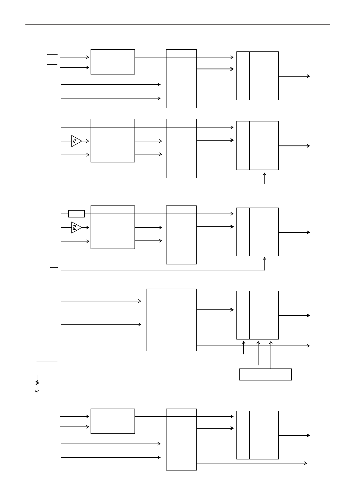
Serial-in-parallel-out driver incorporates a built-in shift register and a latch circuit to control a maximum of 24 LED by a 4-line
interface, linked to a microcontroller.
A single external resistor can set the output current value of the constant current up to a maximum of 50mA. (BD7851FP only)
CMOS open drain output type products can drive the maximum current of 25mA.
●Features
1) LED can be driven directly.
2) Parallel output of a maximum of 24 bit
3) Operational on low voltage (2.7V to 5.5V)
4) Cascade connection is possible (BU2050F and BU2092F,BU2092FV are not acceptable)
●Application
For AV equipment such as, audio stereo sets, videos and TV sets, PCs, control microcontroller mounted equipment.
●Product line-up
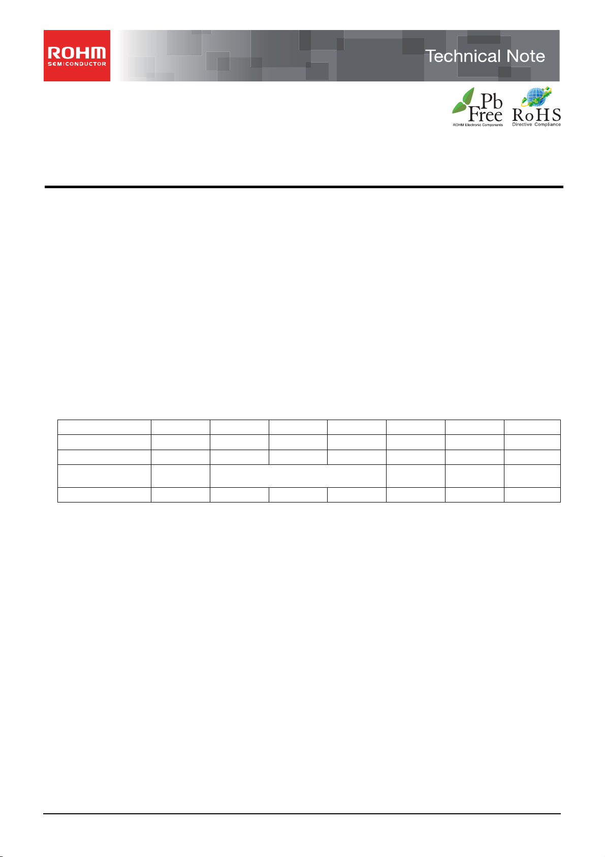
Parameter BU2050F BU2092F BU2092FV BU2099FV BD7851FP BU2152FS Unit
Output current 25 25 25 25 50 25 mA
Output line 8 12 12 12 16 24 line
Output type CMOS Open drain
Package SOP14 SOP18 SSOP-B20 SSOP-B20 HSOP25 SSOP-A32 -
Constant
current
CMOS -
No.09051EAT03
www.rohm.com
© 2009 ROHM Co., Ltd. All rights reserved.
1/24
2009.06 - Rev.A
BU2050F,BU2092F,BU2092FV,BU2099FV,BD7851FP,BU2152FS
Technical Note
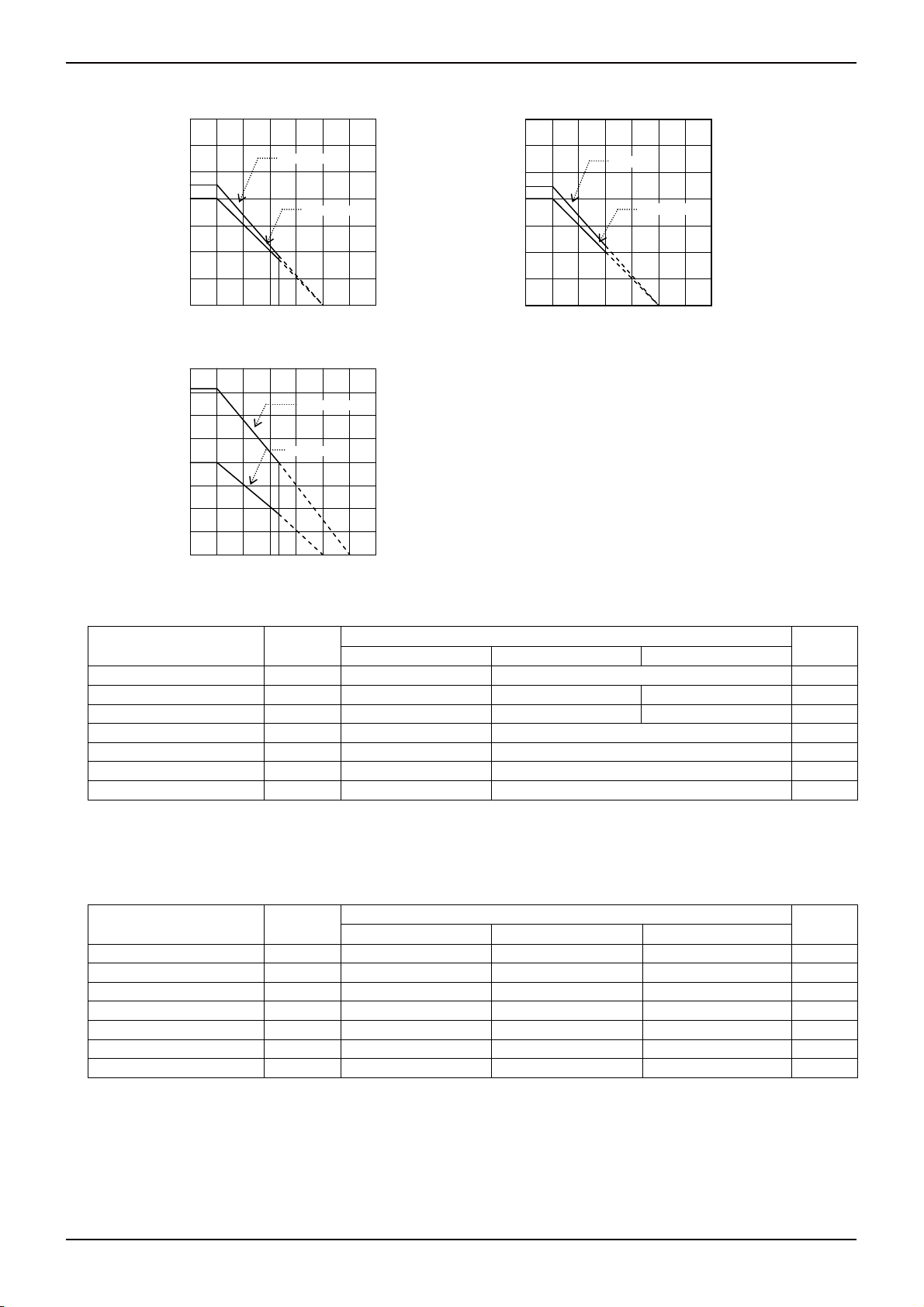
●Thermal derating curve
700
600
500
400
300
BU2050F
BU2099FV
700
600
500
400
300
BU2092F
BU2092FV
200
Power dissipation Pd [mW]
1600
1400
1200
1000
Power dissipation Pd [mW]
100
800
600
400
200
0
25 50
Ambient temperature Ta [℃]
0
25 50
Ambient temperature Ta [℃]
85℃
75 100
85℃
75 100
125 150
BD7851FP
BU2152FS
125 150
175
175
200
Power dissipation Pd [mW]
100
0
25 50
75 100
Ambient temperature Ta [℃]
125 150
175
●Absolute maximum ratings (Ta=25℃)
Parameter Symbol
BU2050F BU2092F BU2092FV
Limits
Unit
Power Supply Voltage VDD -0.3 to +7.0 -0.3 to +7.0 V
Power dissipation 1 Pd1 450 *1 450 (SOP) *2 400 (SSOPB) *3 mW
Power dissipation 2 Pd2 - 550 (SOP) *4 650 (SSOPB) *5 mW
Input Voltage VIN VSS-0.3 to VDD+0.5 VSS-0.3 to VDD+0.3 V
Output Voltage Vo VSS-0.3 to VDD+0.5 VSS to +25.0 V
Operating Temperature Topr -40 to +85 -25 to +75 ℃
Storage Temperature Tstg -55 to +125 -55 to +125 ℃
*1 Reduced by 4.5mW/℃ over 25℃
*2 Reduced by 4.5mW/℃ over 25℃
*3 Reduced by 4.0mW/℃ over 25℃
*4 Reduced by 5.5mW/℃ for each increase in Ta of 1℃ over 25℃ (When mounted on a board 50mm×50mm×1.6mm Glass-epoxy PCB).
*5 Reduced by 6.5mW/℃ for each increase in Ta of 1℃ over 25℃ (When mounted on a board 70mm×70mm×1.6mm Glass-epoxy PCB).
Parameter Symbol
BU2099FV BD7851FP BU2152FS
Limits
Unit
Power Supply Voltage VDD -0.3 to +7.0 0 to +7.0 -0.3 to +7.0 V
Power dissipation 1 Pd1 400 (SSOPB) *6 1450 *7 800 *8 mW
Power dissipation 2 Pd2 650 (SSOPB) *9 - - mW
Input Voltage VIN VSS-0.3 to VDD+0.3 -0.3 to VCC+0.3 VSS-0.3 to VDD+0.3 V
Output Voltage Vo VSS to +25.0 0 to +10 VSS-0.3 to VDD+0.3 V
Operating Temperature Topr -40 to +85 -30 to +85 -25 to +85 ℃
Storage Temperature Tstg -55 to +125 -55 to +150 -55 to +125 ℃
*6 Reduced by 4.5mW/℃ over 25℃
*7 Reduced by 11.6mW/℃ over 25℃
*8 Reduced by 8.0mW/℃ over 25℃
*9 Reduced by 6.5mW/℃ for each increase in Ta of 1℃ over 25℃ (When mounted on a board 70mm×70mm×1.6mm Glass-epoxy PCB).
www.rohm.com
© 2009 ROHM Co., Ltd. All rights reserved.
2/24
2009.06 - Rev.A
BU2050F,BU2092F,BU2092FV,BU2099FV,BD7851FP,BU2152FS
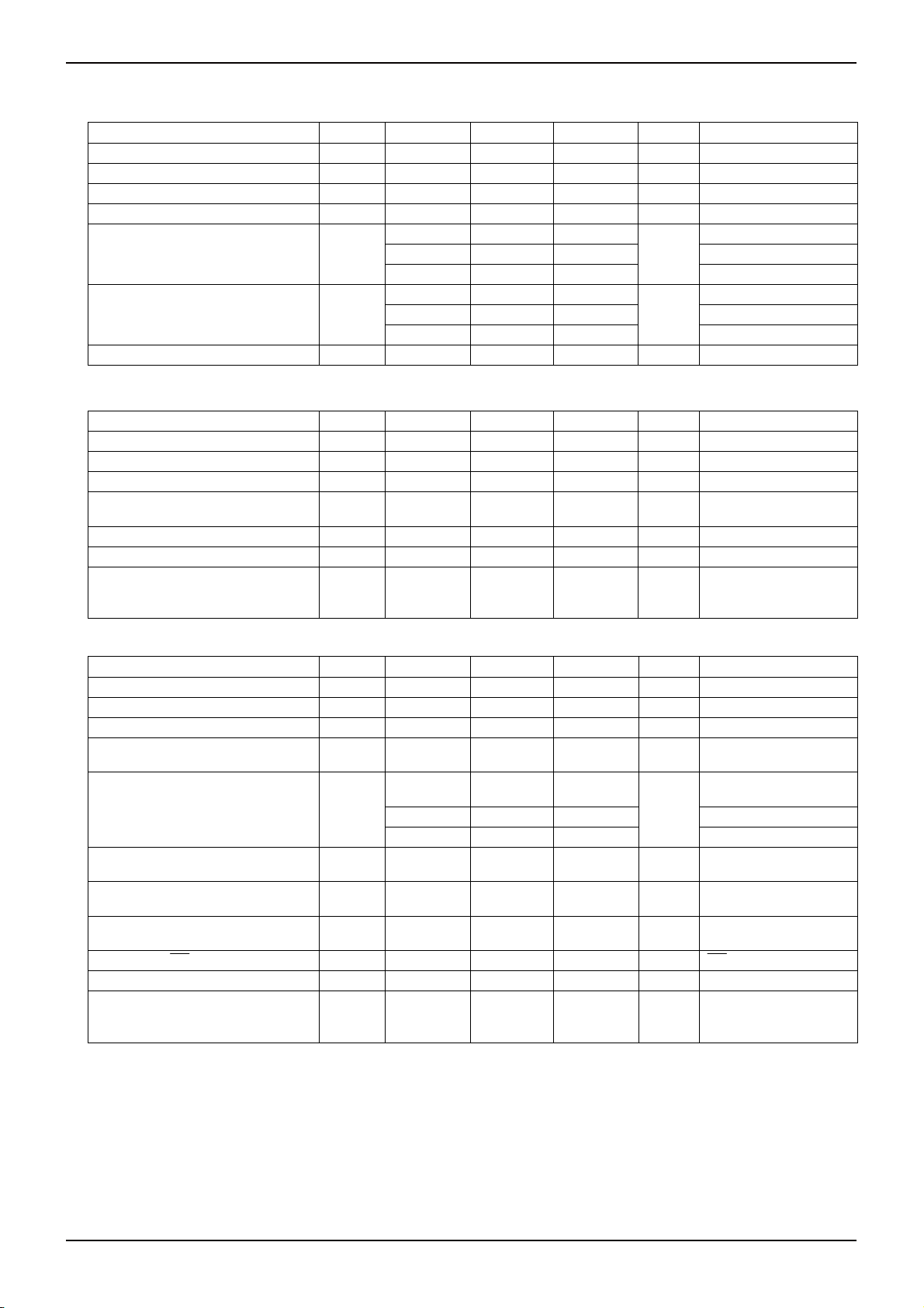
●Electrical characteristics
BU2050F (Unless otherwise noted, Ta=25℃, VDD=4.5 to 5.5V)
Parameter Symbol Min. Typ. Max. Unit Condition
Power Supply Voltage VDD 4.5 - 5.5 V
Input high-level Voltage VIH 0.7VDD - VDD V
Input low-level Voltage VIL VSS - 0.3VDD V
Input Hysteresis VHYS - 0.5 - V
V
DD-1.5 - VDD
Output high-level Voltage VOHD
VDD-1.0 - VDD
V
VDD-0.5 - VDD
V
SS - 1.5
Output low-level Voltage VOLD
VSS - 0.8
V
VSS - 0.4
Quiescent Current IDD - - 0.1 mA
BU2092F/BU2092FV (Unless otherwise noted, Ta=25℃, V
=0V, VDD=5.0V/3.0V)
SS
Parameter Symbol Min. Typ. Max. Unit Condition
Power Supply Voltage VDD 2.7 - 5.5 V
Input high-level Voltage VIH
3.5 / 2.5
- - V
Input low-level Voltage VIL - - 1.5 / 0.4 V
Output low-level Voltage VOL - - 2.0 / 1.0 V
Output high-level disable Current IOZH - - 10.0 μA
Output low-level disable Current IOZL - - -5.0 μA
Quiescent Current IDD - - 5.0 / 3.0 μA
BU2099FV (Unless otherwise noted, Ta=25℃, V
=0V, VDD=5.0V/3.0V)
SS
Parameter Symbol Min. Typ. Max. Unit Condition
Power Supply Voltage VDD 2.7 - 5.5 V
Input high-level Voltage VIH 3.5 / 2.1 - - V
Input low-level Voltage VIL - - 1.5 / 0.9 V
Output high-level Voltage (SO) VOH
V
/ V
DD-0.3
- - V
DD-0.5
- - 1.0
Output low-level Voltage 1 (Qx) VOL1
- - 1.5
V
- - 2.0
Output low-level Voltage 2 (SO) VOL2 - - 0.4 / 0.3 V
Output high-level disable Current
(Qx)
Output low-level disable Current
(Qx)
IPULLDOWN (OE)
OZH - - 10 μA VO=25.0V
I
OZL - - -5.0 μA VO=0V
I
IPD - - 150 / 60 μA
Low Voltage Reset VCLR 1.1 - 2.4 V
Quiescent Current IDD - - 200 μA
Technical Note
IOH=-25mA
IOH=-15mA
OH=-10mA
I
IOL=25mA
IOL=15mA
OL=10mA
I
VIH=VDD, VIL=VSS
DD=5V/3V
V
DD=5V/3V
V
DD=5V/3V,
V
OL=20mA/5mA
I
VO=25.0V
VO=0V
VIN=VSS or VDD
(VDD=5V/3V)
OUTPUT:OPEN
DD=5V/3V
V
VDD=5V/3V
V
DD=5V/3V,
OH=-400μA/-100μA
I
DD=5V/3V,
V
OL1=10mA/5mA
I
DD=5V, IOL1=15mA
V
VDD=5V, IOL1=20mA
DD=5V/3V,
V
OL2=1.5mA/0.5mA
I
OE= VDD, VDD=5V/3V
VIN=VSS or VDD,
VDD=5V
OUTPUT:OPEN
www.rohm.com
© 2009 ROHM Co., Ltd. All rights reserved.
3/24
2009.06 - Rev.A
BU2050F,BU2092F,BU2092FV,BU2099FV,BD7851FP,BU2152FS
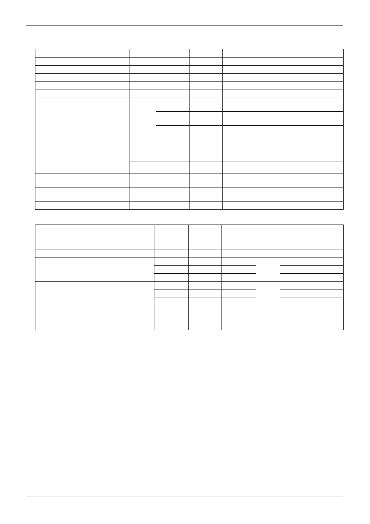
●Electrical characteristics
BD7851FP (Unless otherwise noted, Ta=25℃, VCC=5.0V)
Parameter Symbol Min. Typ. Max. Unit Condition
Power Supply Voltage VDD 4.5 - 5.5 V
Input high-level Voltage VIH
0.8×VCC
- - V
Input low-level Voltage VIL - - 0.2×VCC V
Output high-level Voltage VOH VCC-0.5 - - V
Output low-level Voltage VOL - - 0.5 V
- 0.7 1.0 mA
- 1.8 3.0 mA
Quiescent Current ICC
- 4.0 6.5 mA
- 30 40 mA
Reference Current Output Current
(including the equation between
each bit)
Equation between each bit of
Reference Current Output Current
Change rate of reference current
output current for output voltage
Iolc1 48 55 62 mA
Iolc2 5.0 5.9 6.8 mA VOUT=2.0V, R=13kΩ
Δiolc - ±1 ±6 %
CC - ±1 ±6 %/V
IΔV
Output Leak Current IOH - 0.01 0.8 μA
BU2152FS (Unless otherwise noted, Ta=25℃, V
=2.7 to 5.5V)
DD
Parameter Symbol Min. Typ. Max. Unit Condition
Power Supply Voltage VDD 2.7 - 5.5 V
Input high-level Voltage VIH
2.0
- - V
Input low-level Voltage VIL - - 0.6 V
VDD-1.5 - -
Output high-level Voltage VOH
VDD-1.0 - -
V
VDD-0.5 - -
- - 1.5
Output low-level Voltage VOL
- - 1.0
V
- - 0.8
Quiescent Current IDDST - - 5 μA
Input high-level Current IIH
-
- 1 μA
Input low-level Current IIL - - 1 μA
Technical Note
OH=-1mA
I
IOL=1mA
R=13kΩ
OUT1~OUT16:OFF
R=1.3kΩ
OUT1~OUT16:OFF
R=13kΩ
OUT1~OUT16:ON
R=1.3kΩ
OUT1~OUT16:ON
VOUT=2.0V, R=1.3kΩ
OUTn=2.0V, R=1.3kΩ
V
(1bit : ON)
OUT=2.0 to 3.0V,
V
R=1.3kΩ
VOUT=10V
DD=5V
V
VDD=5V
IOH=-25mA
OH=-15mA
I
IOH=-10mA
IOL=25mA
OL=15mA
I
IOL=10mA
V
IL=VSS, VIH=VDD
www.rohm.com
© 2009 ROHM Co., Ltd. All rights reserved.
4/24
2009.06 - Rev.A
BU2050F,BU2092F,BU2092FV,BU2099FV,BD7851FP,BU2152FS
A
A
A
A
f
●Block diagram
BU2050F
STB
CLR
CLOCK
Controller
Shift
Register
8bit
DAT
BU2092F/BU2092FV
LCK
CLOCK
DAT
Controller
Shift
Register
12bit
OE
BU2099FV
LCK
CLOCK
DAT
LPF
Controller
Shift
Register
12bit
OE
BD7851FP
S_IN
CLOCK
Shift
Register
16bit
LATCH
ENABLE
R_Ire
BU2152FS
STB
CLB
CLOCK
DAT
Controller
Shift
Register
24bit
Technical Note
L
a
t
c
h
L
a
t
c
h
L
a
t
c
h
L
a
t
c
h
Current Adjustment
L
a
t
c
h
Write
Buffer
Write
Buffer
Write
Buffer
Write
Buffer
Write
Buffer
P1~P8
Q0~Q11
Q0~Q11
OUT1~OUT16
SOUT
P1~P24
SO
www.rohm.com
© 2009 ROHM Co., Ltd. All rights reserved.
5/24
2009.06 - Rev.A
BU2050F,BU2092F,BU2092FV,BU2099FV,BD7851FP,BU2152FS
t
t
Technical Note
●Operating description
(1) Data clear
When the reset terminal (CLR, CLB) is set to “L”, the content of all latch circuits are set to “H”, and all parallel outputs are
initialised. (For model with reset terminal only)
(2) Data transfer
Serial data is sequentially input to the shift register during the rise of the clock time (strobe signal is not active). When
the strobe signal is active, the content of the shift register are transferred to the latch circuit.
(3) Cascade connection
Serial input data is output from the serial output through the shift register, regardless of the strobe signal.
(except for BU2050F,
BU2092F/BU2092FV)
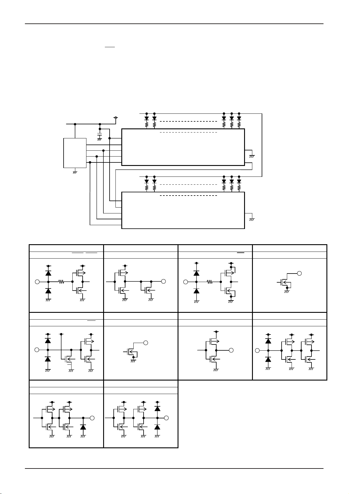
●Application circuit
VDD
MPU
VSS
C1
(*)
VDD
Serial data input
Clock input
Strobe input
Latch input
P1 P2 Pn-2 Pn-1 Pn
VSS
Serial data outpu
VDD
Serial data input
Clock input
Strobe input
Latch input
P1 P2 Pn-2 Pn-1 Pn
VSS
Serial data outpu
(*C1 must be placed as close to the terminal as possible.)
Fig. 1
●Interfaces
BU2050F BU2050F BU2092F/BU2092FV BU2092F/BU2092FV
DATA, CLOCK, STB, CLR P1~P8 DATA, CLOCK, LCK, OE Q0~Q11
V
INPUT
V
DD
DD
OUTPUT
IN
VDD
V
DD
GND(VSS)
GND(VSS)
GND(VSS)
GND(VSS)
GND(VSS)
GND(VSS)
GND(VSS)
BU2099FV BU2099FV BU2099FV BU2152FS
DATA, CLOCK, LCK, OE Q0~Q11 SO CLOCK, DATA, STB, CLB
VDD
VDD
IN
VDD
OUT
V
DD
OUT
VDD
V
DD VDD
GND(VSS)
(only OE pin)
GND(VSS)
GND(VSS)
GND(VSS)
GND(VSS)
GND(VSS)
GND(VSS)
BU2152FS BU2152FS
P1~P28 SO
V
V
DD VDD
DD VDD VDD
VSS
VSS
VSS
GND(VSS)
GND(VSS) GND(VSS)
OUT
GND(VSS)
www.rohm.com
© 2009 ROHM Co., Ltd. All rights reserved.
6/24
2009.06 - Rev.A
BU2050F,BU2092F,BU2092FV,BU2099FV,BD7851FP,BU2152FS
【BU2050F】
●Pin descriptions
Pin No. Pin Name Function
1 P3
2 P4
Parallel Data Output
3 P5
4 VSS GND
5 P6
6 P7
Parallel Data Output
7 P8
8 DATA Serial Data Input
9 CLK Clock Signal Input
Strobe Signal Input
10 STB
In case of “L”, the data of shift register outputs.
In case of “H”, all parallel outputs and data of latch circuit do not change.
Reset Signal Input
11 CLR
In case of “L”, the data of latch circuit reset, and all parallel output (P1~P8) can be L.
Normally CLR=H
12 P1
13 P2
Parallel Data output
14 VDD Power Supply
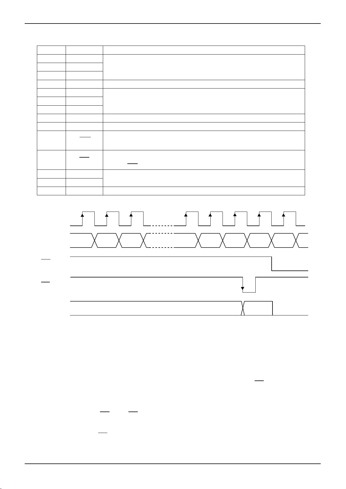
●Timing chart
CLK
Technical Note
DATA
DATA8 DATA7 DATA6 DATA2 DATA1
CLR
STB
Pn
Previous DATA DATA
“L”
Fig. 2
1. After the power is turned on and the voltage is stabilized, STB should be activated, after clocking 8 data bits into the
DATA pin.
th
2. Pn parallel output data of the shift register is set after the 8
clock by the STB.
3. Since the STB is level latch, data is retained in the “L” section and renewed in the “H” section of the STB.
[Function explanation]
・ A latch circuit has the reset function, which is common in all bits. In case of CLR terminal is “L”, the latch
circuit is reset non-synchronously without the other input condition, and all parallel output can be “L”.
・ A serial data inputted from DATA terminal is read in shift register with synchronized rising of clock.
In case of STB is “L” (CLR is ”H”), transmit the data which read in the shift register to latch circuit, and
outputs from the parallel data output terminal (P1~P8).
In case of STB is “H”, all parallel outputs and the data of latch do not change.
www.rohm.com
© 2009 ROHM Co., Ltd. All rights reserved.
7/24
2009.06 - Rev.A
BU2050F,BU2092F,BU2092FV,BU2099FV,BD7851FP,BU2152FS
R
●Switching characteristics (Unless otherwise specified, VDD=4.5 to 5.5V, Ta=25℃)
Parameter Symbol
Min. Typ. Max.
Limit
Unit Condition
Set up time (DATA-CLK) tSD 20 - - ns -
Hold time (DATA-CLK) tHD 20 - - ns -
t
30 - - ns -
Set up time CLK)STB(
Hold time CLK)STB(
Propagation P8)P1CLR( ~
Propagation P8)P1STB( ~
Propagation
P8)P1CLR( ~
Maximum clock frequency f
SSTB
t
30 - - ns -
HSTB
t
- - 100 ns P1~P8 terminal load 20pF or less
PDPCK
t
- - 80 ns P1~P8 terminal load 20pF or less
PDPSTB
t
- - 80 ns P1~P8 terminal load 20pF or less
PDPCLR
5 - - MHz -
MAX
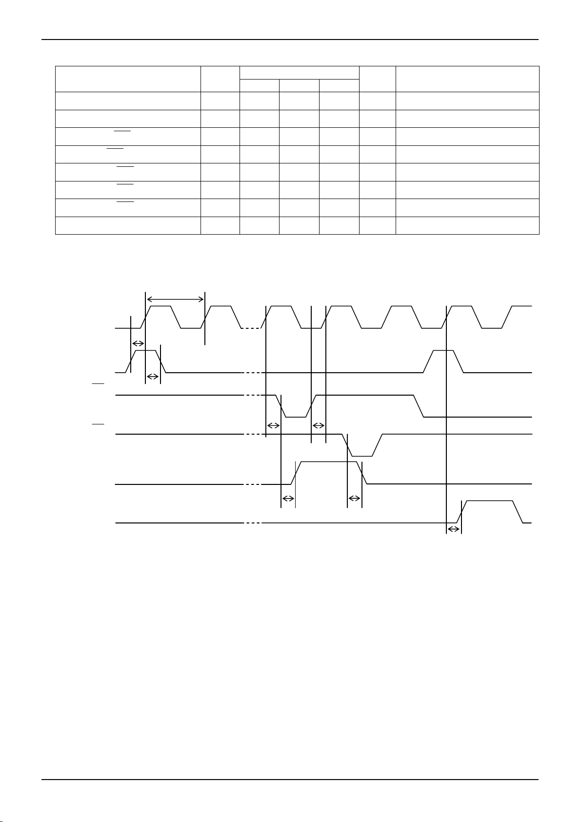
●Switching Time Test Waveform
CLK
tSD
f
MAX
1 2 8 9 10 11 12
DATA
tHD
STB
CLR
t
HSTB
t
SSTB
P8
P1
t
PDPSTB
Fig. 3
t
PDPCL
t
PDPCK
Technical Note
www.rohm.com
© 2009 ROHM Co., Ltd. All rights reserved.
8/24
2009.06 - Rev.A
 Loading...