

Page 1
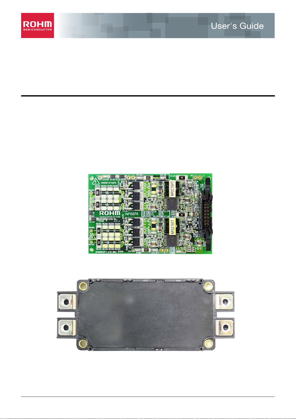
BM60052FV-C Evaluation Board
(For 300 A/1200 V Full-SiC Power Module
Drive)
BM60052FV-EVK-001
1-1. Overview
BM60052FV-EVK-001 (BM60052FV-C Evaluation Board) is an evaluation board whose shape allows direct mounting onto
the ROHM’s 2ch 300 A/1200 V class full-SiC power module, BSM300D12P2E001.
This is a single unit, comprising the SiC-MOSFET gate drive circuit along with the gate driver IC, the BM60052FV-C
integrating insulation element, and an insulated DC-DC converter, supplying gate voltage.
The constant is set to the value suitable for driving BSM300D12P2E001.
Integrated functions include SiC-MOSFET’s DESAT detection function, soft turn-off function at DESAT detection, DESAT
detection FLT signal output function, gate bias voltage reduction detection/gate state monitoring RDY signal output function,
and mirror clamp function.
This evaluation board is intended to be used with BM60052FV-C to drive the full-SiC power module for evaluation. However,
it is not designed for mass-production use.
1-2. Schematic of the board
[BM60052FV-EVK-001]
Reference: [Full-SiC Power Module BSM300D12P2E001]: To be purchased separately
www.rohm.co.jp
© 2016 ROHM Co., Ltd. All rights reserved.
1/9
2016.3.4 Rev.002
Page 2

Datasheet
BM60052FV-EVK-001
Datasheet
2-1. Performance specifications (Ta=25°C. These are typical values and do not guarantee the characteristics of the
evaluation board.)
Power voltage
Power current
Number of drive circuits 2
Range of input signal frequency DC ~ 100 kHz
Minimum input ON pulse width 1.0 µs * 6
Minimum input OFF pulse width 1.0 µs
Input signal 5V 0-P
Maximum gate drive charge 1500 nC * 1, * 2
Output forward bias voltage (+Vg) +17 V ~ +19 V * 1
Output reverse bias voltage (-Vg) -3 V ~ -5 V * 1
Gate forward direction bias current (+Ig) +7.5 A max (Prw 0.5 µs) * 1, * 2
Characteristic item Standard/Rating Remarks
12 VDC ~ 28 VDC (15 V typ., 24 V typ.) between Pin1
and Pin2
0.8 A (power voltage 15 VDC)
0.5 A (power voltage 24 VDC)
* 1
Gate drawing current (-Ig) -8.5 A max (Pfw 0.5 µs) * 1, * 2
Rise response delay time (+Tstg) 100 ns typ. * 1, * 3
Fall response delay time (-Tstg) 100 ns typ. * 1, * 4
Rise time (Tr) 100 ns typ. * 1, * 5
Fall time (Tf) 100 ns typ. * 1, * 5
Withstand voltage For one minute at AC 2500 V (between input and output)
Repeatedly peak voltage
1200V voltage betweenTH7 and TH8, voltage between
TH8 and TH8
Insulation resistance 100 m or more at DC 500 V (between input and output)
DESAT detection voltage 4.0 V (min)
Operating temperature range -40 ~ +70ºC
Storage temperature range -40 ~ +80ºC
Operating humidity range 30% to 90% RH (No dew-condensation)
* 1 Vin: 15 V, 24 V; Load: Dummy load equivalent to BSM300D12P2E001, i.e., 1.6 + 0.083 µf; f: 100 kHz and Duty
cycle: 50%
* 2 A gate resistance (RG) of 0.2 is inserted in the circuit for SiC-MOSFET gate driver as shown in the following
figure.
www.rohm.co.jp
© 2016 ROHM Co., Ltd. All rights reserved.
Gate driver
ゲートドラ イ バー
RG= 0.2 Ω
RG= 0.2 Ω
2/9
SiC-MOSFET
G
Vg
S
2016.3.4 Rev.002
Page 3
Datasheet
BM60052FV-EVK-001
g
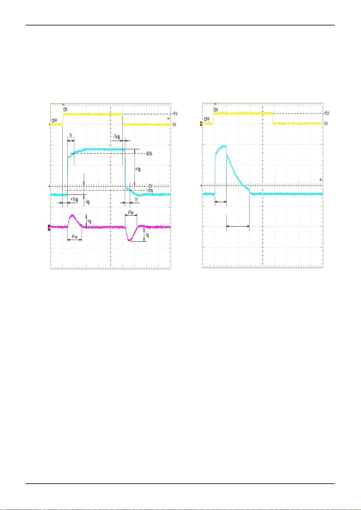
* 3 +Tstg: The time from the rise of input signals until reaching 10% of the output gate signal peak value.
* 4 -Tstg: The time from the fall of input signals until reaching 90% of the output gate signal peak value.
* 5 Tr, Tf: The time taken for the transition between 10% and 90% of the output gate signal peak value.
* 6 About 1 µs is defined for DESAT detection suppression after the gate rise.
2-2. Definition of output parameters
(1) At steady output (2) At DESAT detection
Datasheet
Input signal
Output signal
Gate current
Input signal
Output si
nal
Short-circuit detection
suppression time
1 s typ
Soft turn-off
www.rohm.co.jp
© 2016 ROHM Co., Ltd. All rights reserved.
3/9
2016.3.4 Rev.002
Page 4
Datasheet
BM60052FV-EVK-001
Datasheet
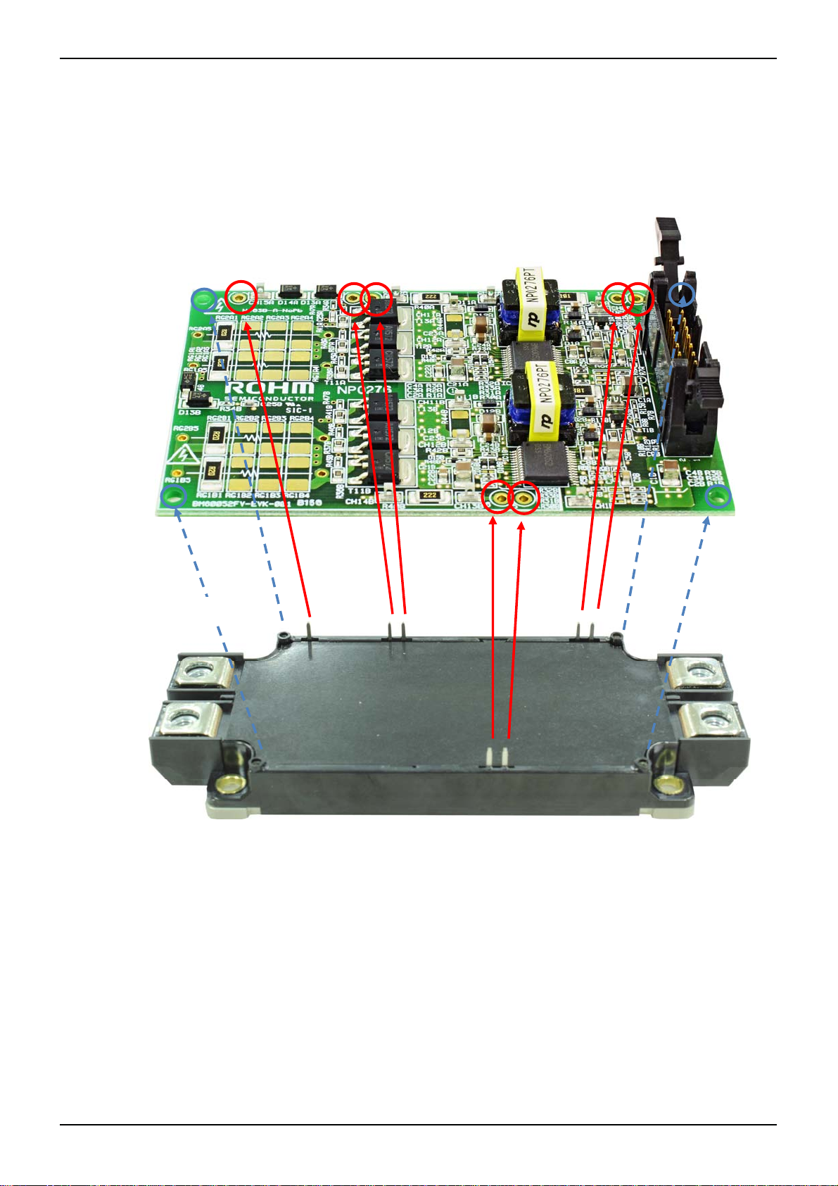
3. Operating procedures
(1) Place BM60052FV-EVK-001 on the full-SiC power module and make sure that the seven pins are correctly located.
(See the red solid lines in the following figure)
(2) Fix BM60052FV-EVK-001 using self-tap screws. (See the blue dotted lines in the following figure)
(3) Solder the seven pins for electrical connection.
[BM60052FC-EVK-001]
[BSM300D12P2E001]
www.rohm.co.jp
© 2016 ROHM Co., Ltd. All rights reserved.
4/9
2016.3.4 Rev.002
Page 5

Datasheet
BM60052FV-EVK-001
4-1. Block diagram (check pin configuration)
Stabilizing
circuit
To e ach
circuit
Datasheet
converter
Short-circuit
detection circuit
UVLO
circuit
To e ach
circuit
Gate drive circuit
To e ach
circuit
Gate state monitoring
and soft turn-off circuit
Mirror clamp
circuit
Upper arm side
Connector
4-2. Description of check pins
CH15A
SiC power module
Upper arm drain voltage
CH11A
Upper arm DC-DC converter
Secondary +18 V
CH12A
Upper arm DC-DC converter
Secondary-4 V
CH11B
Lower arm DC-DC converter
Secondary +18 V
Stabilizing
To e ach
CH13A
SiC power module
Upper arm gate voltage
circuit
circuit
converter
Short-circuit
detection circuit
UVLO
circuit
To e ach
circuit
Gate drive circuit
To e ach
circuit
Gate state monitoring
and soft turn-off circuit
Mirror clamp
circuit
Lower arm side
Connection side
with power module
CH14A
SiC power module
Upper arm source voltage
Lower arm drain voltage
Upper arm DC-DC converter
secondary GND
CH2A
Upper arm DC-DC converter
Main FET drain voltage
CH1A
Primary
GND
CH2B
Lower arm DC-DC converter
Main FET drain voltage
CH12B
Lower arm DC-DC converter
Secondary-4 V
CH14B
SiC power module
Lower arm source voltage
Lower arm DC-DC converter
secondary GND
CH13B
SiC power module
Lower arm gate
voltage
CH1B
Primary
GND
* Yellow: Primary, Red: Secondary upper arm side, Blue: Secondary lower arm side
The oscilloscope power supply should be floating. When measuring circuits with different GND potentials simultaneously, use
a differential probe or other device to prevent ground fault or short circuit in the oscilloscope’s GND terminal.
www.rohm.co.jp
© 2016 ROHM Co., Ltd. All rights reserved.
5/9
2016.3.4 Rev.002
Page 6
Datasheet
BM60052FV-EVK-001
5-1. Through-hole pin layout, connector layout
5-2. Names of input/output terminals
Power supply, signal input/output:
HIF3BA-14PA-2.54DSA (71) (Hirose Electric)
(Connector side: CN 1-14)
CN
1
TH [7] TH [8] [9]
Signal
name
VDD
Description TH
Input power (+12 V ~+28 V)
TH [10] [11]
TH [6] [5]
Gate source output, drain input: 2.0 mm through
hole
(Connection side with power module: upper figure [5]
to [11])
Signal
name
5
S-B
Description
B ch source output
Datasheet
Connector
(CN)
14 13
12 11
10 9
8 7
6 5
4 3
2 1
2
3
4
5
6
7
8
9
10
11
12
13
14
A_XXX: A ch-related upper arm control-associated terminal
B_XXX: B ch-related lower arm control-associated terminal
GND
B_INA
B_INB
B_ENA
B_FLT
B_RDY
A_INA
A_INB
A_ENA
A_FLT
A_RDY
TH2
TH1
Input power (GND) 6
B ch input signal A 7
B ch input signal B 8
B ch enable signal
B ch short circuit detection output
B ch UVLO, gate state monitoring
output
A ch input signal A 11
A ch input signal B X_A: Element-related terminal for upper arm
A ch enable signal X_B: Element-related terminal for lower arm
A ch short-circuit detection output
A ch UVLO, gate state monitoring
output
Thermistor terminal 11 (not used)
Thermistor terminal 10 (not used)
10
G-B
D-A
S-A
/D-B
9
For the thermistor terminals, TH1 and TH2 are only
connected to each other on the substrate, and not to
the IC.
G-A
TH1
TH2
B ch gate output
A ch drain input
A ch source output
and B ch drain input
A ch gate output
Thermistor terminal 10 (not used)
Thermistor terminal 11 (not used)
www.rohm.co.jp
© 2016 ROHM Co., Ltd. All rights reserved.
6/9
2016.3.4 Rev.002
Page 7
Datasheet
BM60052FV-EVK-001
5-3. Fitting connectors
Hirose Electric Omron
Flat cable pressure welding-type
HIF3BA-14D-2.54R XG4M-1430-T
Datasheet
connector
Loose-wire crimp-type connector HIF3BA-14D-2.54C XG5N-141
Contact for loose wires HIF3-2226SC(AWG22~AWG26) XG5W-0231(AWG22~26)
HIF3-2428SC(AWG24~AWG28) XG5W-0232(AWG24~28)
Note: For details, refer to the manufacturer’s catalog.
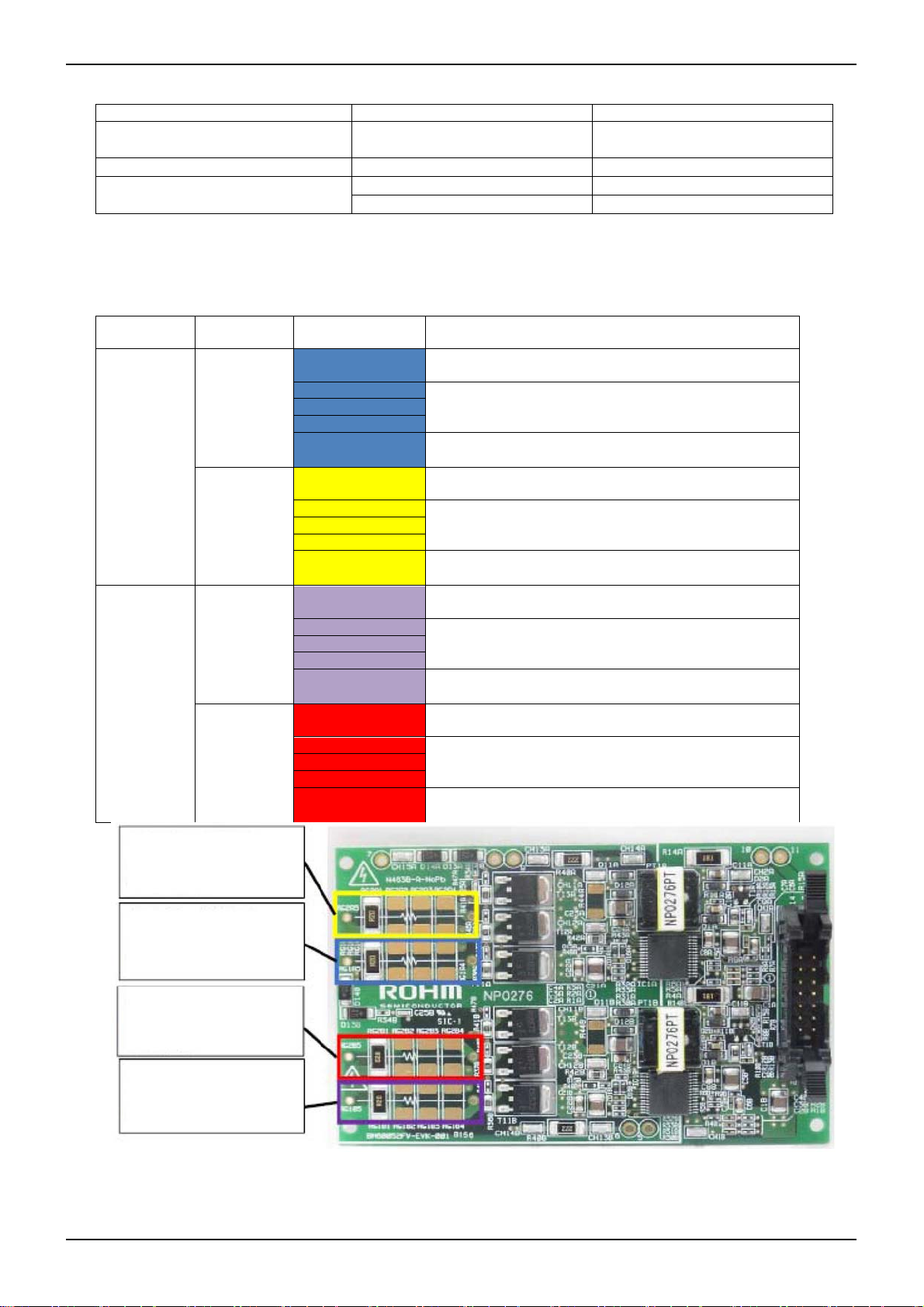
6. Selection of gate resistance
The gate resistance of this product is 0.2 , which is a standard level for BSM300D12P2E001. This can be
changed to an optimum value according to your equipment. Make the required adjustment by paying attention
to the operation and heat generation in each part.
Upper/
lower arms
Upper arm
side
Lower arm
side
Rise
5-parallel
connection
Fall
5-parallel
connection
Rise
5-parallel
connection
Fall
5-parallel
connection
Circuit symbol Substrate pattern layout/Implementation status
RG1A1 Square shape chip resistor MCR100 (1 W_0.2 J,
ROHM): Implemented
RG1A2
RG1A3
RG1A4
RG1A5
RG2A1 Square shape chip resistor MCR100 (1 W_0.2 J,
RG2A2
RG2A3
RG2A4
RG2A5
RG1B1 Square shape chip resistor MCR100 (1 W_0.2 J,
RG1B2
RG1B3
RG1B4
RG1B5
RG2B1 Square shape chip resistor MCR100 (1 W_0.2 J,
RG2B2
RG2B3
RG2B4
RG2B5
Square shape chip resistor MCR100 (1 W, ROHM): Not
implemented
Through-hole diameter φ1.2 mm and pitch 25.4 mm: Not
implemented
ROHM): Implemented
Square shape chip resistor MCR100 (1 W, ROHM): Not
implemented
Through-hole diameter φ1.2 mm and pitch 25.4 mm: Not
implemented
ROHM): Implemented
Square shape chip resistor MCR100 (1 W, ROHM): Not
implemented
Through-hole diameter φ1.2 mm and pitch 25.4mm: Not
implemented
ROHM): Implemented
Square shape chip resistor MCR100 (1 W, ROHM): Not
implemented
Through-hole diameter φ1.2 mm and pitch 25.4 mm: Not
implemented
RG2A1 ~ RG2A5
Upper arm fall side
5-parallel connection
RG1A1 ~ RG1A5
Upper arm rise side
5-parallel connection
RG2B1 ~ RG2B5
Upper arm fall side
5-parallel connection
RG1B1 ~ RG1B5
Lower arm rise side
5-parallel connection
The recommended minimum gate resistance value is 0.2 .
Increasing the gate resistance value will increase switching loss of the SiC power module, which may adversely affect
the expected performance. Thus, a gate resistance as small as possible should be chosen.
www.rohm.co.jp
© 2016 ROHM Co., Ltd. All rights reserved.
7/9
2016.3.4 Rev.002
Page 8

Datasheet
BM60052FV-EVK-001
7. Description of each function
Input signal and enable signal, determine the output logic.
CN10: A_ENA
CN5: B_ENA
L x x L
H H x L
H L L L
H L H H
Logic H and L level input voltages are in the range 2.0 V ~ 5.5 V and 0 ~ 0.8 V, repectively.
CN9: A_INB
CN4: B_INB
CN8: A_INA
CN3: B_INA
Datasheet
TH[9]: G-A (gate output)
TH[6]: G-B (gate output)
CH1 (yellow, 2.0 V/div): INA
CH2 (light blue, 2.0 V/div): INB
CH3 (pink, 5.0 V/div): Gate output
t: 2 µs/div
DESAT detection, FLT signal output (A_FLT, B_FLT)
When the gate output is high and SiC-MOSFET's Vds is 4V or more, the gate voltage is lowered (soft turn-off) and FLT
signals (8-pin) are output. (0 V at detection and 4 V at steady state).
This operation is cleared at the rise of input signal ENA.
The FLT terminal is pulled up with the VREG terminal on the evaluation substrate at 10 k.
A detection suppression time of about 1 µs is defined after the gate rise.
For details of the DESAT detection function, refer to the data sheet of BM60052FV-C.
Gate bias voltage reduction detection (UVLO), gate state monitoring, RDY signal output (A_RDY, B_RDY)
When the gate bias voltage approximate 18V is decreased to approximate14V because of abnormalities such as gate
output short-circuit and an output over current, or the gate state monitoring finds an inconsistency between the input
and output, a RDY signal will be output (0 V at detection and 4 V at steady state).
When the power voltage increases to the voltage reduction detection level, the operation returns to the steady state.
The RDY terminal is pulled up with the VREG terminal on the evaluation substrate at 10 k.
Gate state monitoring filter time: 1.5 µs ~ 2.5 µs
Mirror clamp function
While the gate output is low, when the OUT2 terminal falls below a certain voltage level, the mirror clamp function starts
operating. Also, it starts operating at DESAT detection.
Mirror clamp detection voltage: 1.8 V ~ 2.2 V (between G and S)
For details of the mirror clamp function, refer to the data sheet of BM60052FV-C.
Thermal protection function
BM60052FV-C has temperature sensor voltage input terminals and integrates the thermal protection function. However,
these are set up as unavailable for this evaluation board.
(The connection hole of the module is connected to the connector and not to BM60052FV-C.)
www.rohm.co.jp
© 2016 ROHM Co., Ltd. All rights reserved.
8/9
2016.3.4 Rev.002
Page 9
Datasheet
BM60052FV-EVK-001
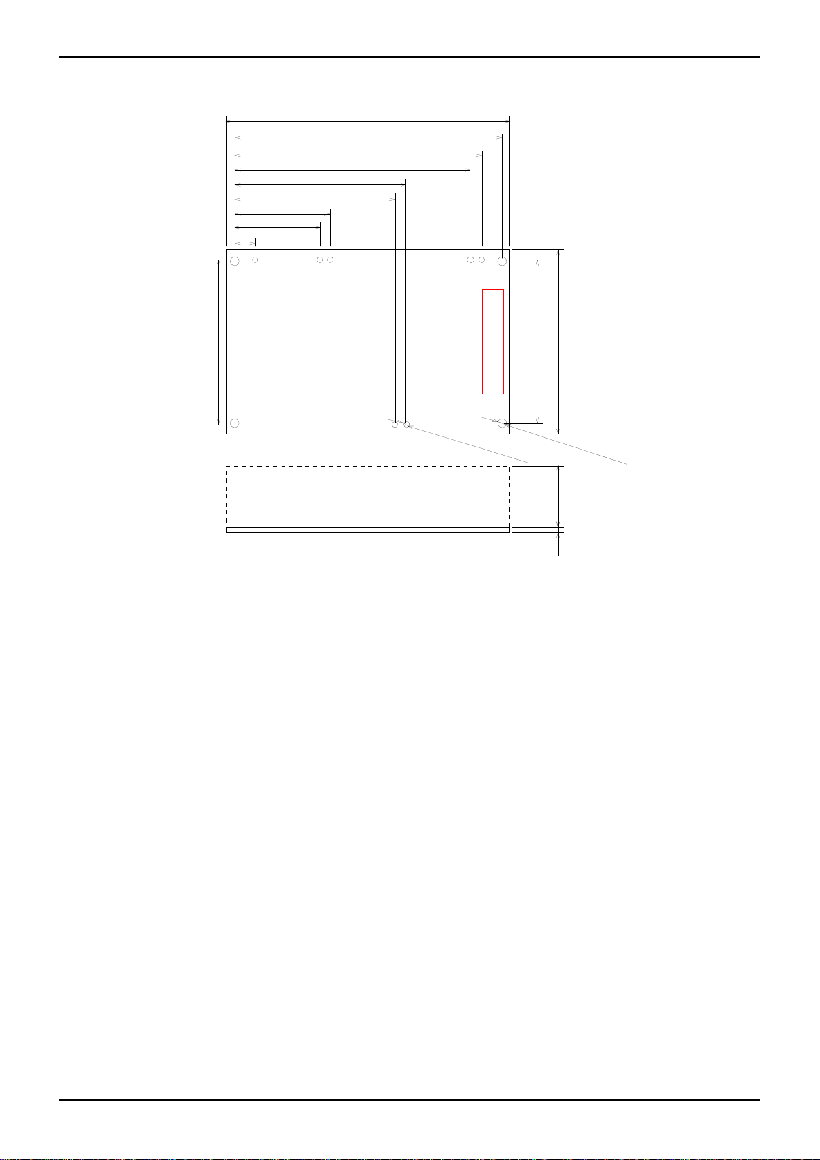
7. Outline drawing
58.4
7.25
30 .11
7
33.9
100
94.5
87.26
83.45
6 0.58
56.77
8 9 10 11
65
Datasheet
13
14
CN1:
H IF3BA- 14PA-2.54D SA1
2
7
-
φ
2
.
0
65
57.5
4
-
φ
2
.
8
N
T
H
1.6 TBD
T
H
Unit (mm)
(mm)
単位
Tolerance 1 mm
1mm
公差±
www.rohm.co.jp
© 2016 ROHM Co., Ltd. All rights reserved.
9/9
2016.3.4 Rev.002
Page 10

■<High Voltage Safety Precautions>
◇ Read all safety precautions before use
Please note that this document covers only the BM60052FV-C evaluation board
(BM60052FV-EVK-001) and its functions.
For additional information, please refer to the datasheet.
To ensure safe operation, please carefully read all precautions
before handling the evaluation board
Depending on the configuration of the board and voltages used,
Potentially lethal voltages may be generated.
Therefore, please make sure to read and observe all safety precautions
described in the red box below.
Notice
Before Use
[1] Verify that the parts/components are not damaged or missing (i.e. due to the drops).
[2] Check that there are no conductive foreign objects on the board.
[3] Be careful when performing soldering on the module and/or evaluation board to ensure
that solder splash does not occur.
[4] Check that there is no condensation or water droplets on the circuit board.
During Use
[5] Be careful to not allow conductive objects to come into contact with the board.
[6] Brief accidental contact or even bringing your hand close to the board may result
in discharge and lead to severe injury or death.
Therefore, DO NOT touch the board with your bare hands or bring them too close
to the board.
In addition, as mentioned above please exercise extreme caution when using
conductive tools such as tweezers and screwdrivers.
[7] Please proceed carefully, taking note of any condensation when operating at low
temperatures or discoloration/leakage of the parts/board due to excessive heat.
[8] Be sure to wear insulated gloves when handling is required during operation.
After Use
[9] Even after the power has been turned off, please note that burns can still occur due to
contact with superheated parts or electric shock caused by charge stored in the
capacitor.
[10] Protect against electric shocks by wearing insulated gloves when handling.
This evaluation board is intended for use only in research and development facilities and
should by handled
only by qualified personnel familiar with all safety and
operating procedures.
We recommend carrying out operation in a safe environment that includes the use of high
voltage signage at all entrances, safety interlocks, and protective glasses.
www.rohm.com
©2015ROHMCo.,Ltd.Allrightsreserved.
Page 11

Notes
1)
The information contained herein is subject to change without notice.
2)
Before you use our Products, please contact our sales representative and verify the latest specifications :
3)
Although ROHM is continuously working to improve product reliability and quality, semiconductors can break down and malfunction due to various factors.
Therefore, in order to prevent personal injury or fire arising from failure, please take safety
measures such as complying with the derating characteristics, implementing redundant and
fire prevention designs, and utilizing backups and fail-safe procedures. ROHM shall have no
responsibility for any damages arising out of the use of our Poducts beyond the rating specified by
ROHM.
4)
Examples of application circuits, circuit constants and any other information contained herein are
provided only to illustrate the standard usage and operations of the Products. The peripheral
conditions must be taken into account when designing circuits for mass production.
5)
The technical information specified herein is intended only to show the typical functions of and
examples of application circuits for the Products. ROHM does not grant you, explicitly or implicitly,
any license to use or exercise intellectual property or other rights held by ROHM or any other
parties. ROHM shall have no responsibility whatsoever for any dispute arising out of the use of
such technical information.
6)
The Products are intended for use in general electronic equipment (i.e. AV/OA devices, communication, consumer systems, gaming/entertainment sets) as well as the applications indicated in
this document.
7)
The Products specified in this document are not designed to be radiation tolerant.
8)
For use of our Products in applications requiring a high degree of reliability (as exemplified
below), please contact and consult with a ROHM representative : transportation equipment (i.e.
cars, ships, trains), primary communication equipment, traffic lights, fire/crime prevention, safety
equipment, medical systems, servers, solar cells, and power transmission systems.
9)
Do not use our Products in applications requiring extremely high reliability, such as aerospace
equipment, nuclear power control systems, and submarine repeaters.
10)
ROHM shall have no responsibility for any damages or injury arising from non-compliance with
the recommended usage conditions and specifications contained herein.
11)
ROHM has used reasonable care to ensur the accuracy of the information contained in this
document. However, ROHM does not warrants that such information is error-free, and ROHM
shall have no responsibility for any damages arising from any inaccuracy or misprint of such
information.
12)
Please use the Products in accordance with any applicable environmental laws and regulations,
such as the RoHS Directive. For more details, including RoHS compatibility, please contact a
ROHM sales office. ROHM shall have no responsibility for any damages or losses resulting
non-compliance with any applicable laws or regulations.
13)
When providing our Products and technologies contained in this document to other countries,
you must abide by the procedures and provisions stipulated in all applicable export laws and
regulations, including without limitation the US Export Administration Regulations and the Foreign
Exchange and Foreign Trade Act.
14)
This document, in part or in whole, may not be reprinted or reproduced without prior consent of
ROHM.
Notice
Thank you for your accessing to ROHM product informations.
More detail product informations and catalogs are available, please contact us.
ROHM Customer Support System
www.rohm.com
© 2015 ROHM Co., Ltd. All rights reserved.
http://www.rohm.com/contact/
R1102
A
 Loading...