

Class-AB Speaker Amplifiers
1W+1W Stereo
Speaker / Headphone Amplifier
BH7884EFV
●Description
The BH7884EFV is a low voltage, low noise, high output speaker and headphone amplifier drive, in which a Bi-CMOS
process is used. This IC supports: headphone amplifier gain adjustment, active/suspend switching, speaker amplifier
stereo/monaural switching, and amplifier mute switching. All functions are controllable from a microcontroller. Built-in digital
noise reduction circuits eliminate digital noise and BEEP sounds.
●Features
1) Built-in 1W+1W stereo speaker amplifier (Vcc=5V, RL=8, THD=10%)
2) Built-in stereo headphone amplifier
3) Built-in bass boost function for speaker amplifier
4) Built-in low noise VCA (electronic volume) for headphone
5) Built-in mute circuit
6) Built-in standby circuit
7) Low current consumption specifications (9 mA TYP. in ACTIVE mode, 0.2 A TYP. in SUSPEND mode)
●Applications
Notebook computers, LCD TVs, etc.
●Absolute maximum ratings(Ta=25℃)
Parameter Ratings Unit
No.10077EAT06
Supply voltage +6.0 V
Power dissipation 1100 *1 mW
Storage temperature -55 ~ +125 ℃
Operating temperature -10 ~ +70 ℃
*1 Reduced by 11 mW/℃ at 25℃ or higher, when mounting on a 70mmX70mmX1.6mm PCB board).
●Operating Conditions (Ta=25℃)
Parameter Ratings Unit
Supply voltage +3.0~+5.5 V
* This IC is not designed to be radiation-resistant.
www.rohm.com
© 2010 ROHM Co., Ltd. All rights reserved.
1/10
2010.06 - Rev.A
/
/
/
/
/
BH7884EFV
●Electrical characteristics (Unless otherwise noted, VCC=3.3V, Ta=25℃, f=1kHz)
Parameter Symbol
Min. Typ. Max.
Limits
Unit Condition
■1 CHIP
Circuit current ACTV IA - 9.0 18.0 mA No signal ACTIVE
Circuit current SPND Is - 0.2 10.0 µA No signal SUSPEND
■SP AMP
Voltage gain1 GSP1 9.0 12.0 15.0 dB SE, Vin=-18dBV,RL=8Ω
Voltage gain2 GSP2 15.2 18.2 21.2 dB BTL, Vin=-18dBV
Distortion DSP - 0.1 1.0 % BTL, Vin=-18dBV
Technical Note
Maximum output level V
Output noise level V
2.2 5.2 - dBV BTL, DSP=1%
OSP
- -97 -80 dBV SE, DIN-Audio
NSP
Cross talk CTSP - -90 -80 dBV SE, Vin=-18dBV, DIN-Audio
Output level on mute MTSP - -102 -80 dBV BTL, Vin=-18dBV
■HP AMP
Voltage gain 3 GHP 2.6 5.6 8.6 dB VOL:MAX, RL=10kΩ,Vin=-12dBV
Voltage gain 4 GHP -10 -7 -4 dB VOL:MAX, RL=32Ω,Vin=-12dBV
Distortion DHP - 0.025 0.1 % VOL:MAX, RL=32Ω,Vin=-8dBV
Variable width of volume ΔGHP 70 100 - dB VOL:MIN ~ MAX, RL=32Ω
Maximum output level V
Output noise level V
Cross talk CTHP - -98 -80 dBV
Output level on mute MTHP - -110 -80 dBV
-2.0 1.0 - dBV VOL:MAX, DHP=1%, RL=10kΩ
OHP
- -98 -80 dBV VOL:MAX, RL=32Ω, DIN-Audio
NHP
VOL:MAX, R
=32Ω,Vin=-12dBV
L
DIN-Audio
VOL:MAX, R
=32Ω,Vin=-12dBV
L
DIN-Audio
■BEEP AMP
Output voltage level VBP 0.8 1.25 - Vpp Vin=1.3dBV, f=1kHz, 20MHzLPF
■BIAS
Output voltage level V
1.4 1.7 2.0 V No Signal
BIAS
■CTRL
ACTIVE mode V
SUSPEND mode V
VCC-0.3 - VCC V
11H
GND - 0.3 V
11L
SP/ON mode V2H VCC-0.3 - VCC V
SP/OFF mode V2L GND - 0.3 V
BASS-BOOST/ON mode V4H VCC-0.7 - VCC V
BASS-BOOST/OFF mode V4L GND - 0.7 V
STEREO mode V3H VCC-0.7 - VCC V
MONO mode V3L GND - 0.7 V
ACTIVE mode V
MUTE mode V
VCC-0.7 - VCC V
10H
GND - 0.7 V
10L
■PSRR
Ripple rejection ratio GPR - -64 - dBV
www.rohm.com
© 2010 ROHM Co., Ltd. All rights reserved.
2/10
Active mode.
Hold Voltage of 11pin.
Suspend mode.
Hold Voltage of 11pin.
ON mode.
SP
Hold Voltage of 2pin.
SP/OFF mode.
Hold Voltage of 2pin.
SP/Bass Boost mode.
Hold Voltage of 4pin.
Non Boost mode.
SP
Hold Voltage of 4pin.
SP/STEREO mode.
Hold Voltage of 3pin.
MONO mode.
SP
Hold Voltage of 3pin.
Active mode.
HP
Hold Voltage of 10pin.
MUTE mode.
HP
Hold Voltage of 10pin.
f=100Hz, 0.3Vpp, SIN Input
SPOUT monitor, DIN-Audio
2010.06 - Rev.A
BH7884EFV
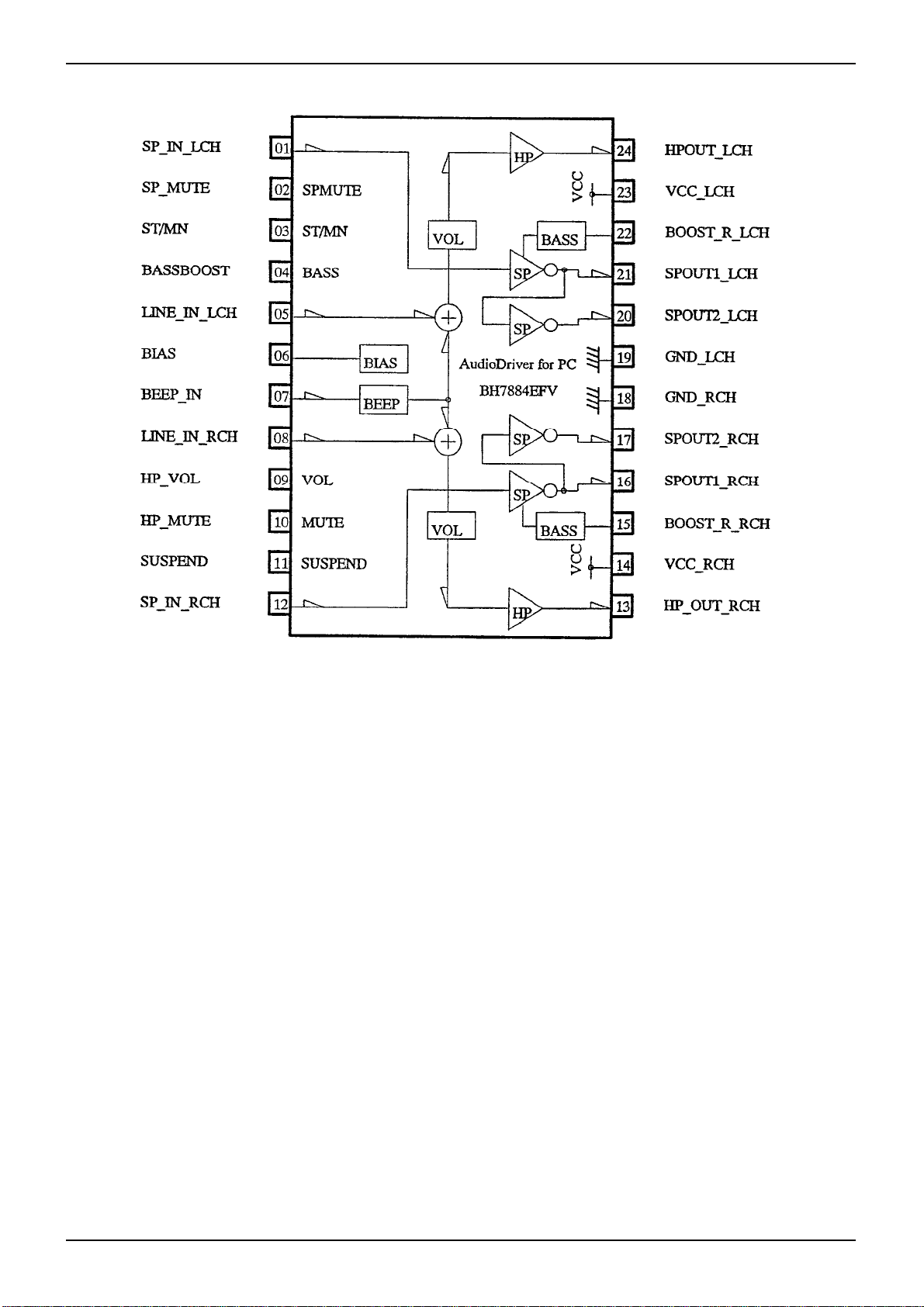
●Block diagram
Technical Note
Fig.1
www.rohm.com
© 2010 ROHM Co., Ltd. All rights reserved.
3/10
2010.06 - Rev.A
BH7884EFV
●Control pin settings
H SP ACTIVE SPAMP is in active state
L SP MUTE SPAMP is in suspend state
H STEREO For SPAMP, LCH and RCH both are in active state
L MONO For SPAMP, LCH is in active state and RCH is in suspend state
H BASS BOOST For SPAMP, bass is boosted
L NON -BOOST For SPAMP, bass is not boosted
H ACTIVE HPAMP is in active state
L MUTE HPAMP is in mute state
Technical Note
SP MUTE PIN:2PIN
STEREO/MONO PIN:3PIN
BASSBOOST PIN:4PIN
MUTE PIN:10PIN
(The SPAMP mute function is realized by connecting HP_OUT to SP_IN)
SUSPEND PIN:11PIN
H ACTIVE The IC is in active state
L SUSPEND The IC is in suspend state
www.rohm.com
© 2010 ROHM Co., Ltd. All rights reserved.
4/10
2010.06 - Rev.A
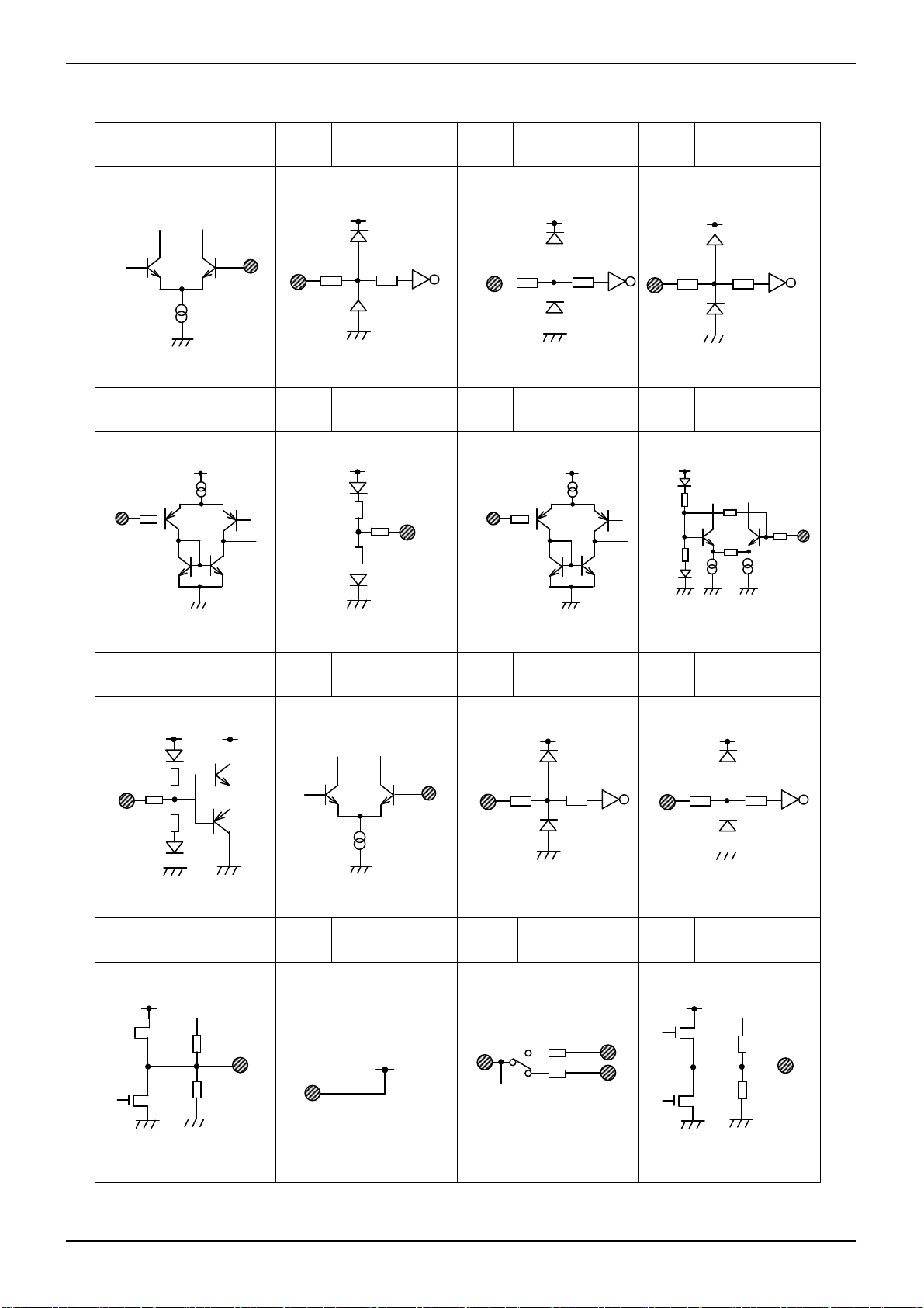
BH7884EFV
Technical Note
●Equivalent circuit
PIN1 SP_IN_LCH PIN2 SP_MUTE PIN3 ST/MN PIN4 BASS BOOST
100k
100k
100k
100k
100k
100k
PIN5 LINE_IN_LCH PIN6 BIAS PIN7 BEEP_IN PIN8 LIHE_IN_RCH
50
50k
35k
100k
50
16k
60k
47k
27k
PIN9 HP_VOL PIN10 HP_MUTE PIN11 SUSPEND PIN12 SP_IN_RCH
100k
1k
100k
100k
100k
100k
100k
PIN13 HP_OUT_RCH PIN14 VCC_RCH PIN15 BOOST_R_RCH PIN16 SPOUT1_RCH
25k
7.5k
12
40k
40k
16
15
25k
7.5k
www.rohm.com
© 2010 ROHM Co., Ltd. All rights reserved.
5/10
2010.06 - Rev.A

BH7884EFV
Technical Note
PIN17 SPOUT2_RCH PIN18 GND_RCH PIN19 GND_LCH PIN20 SPOUT2_LCH
25k
7.5k
25k
7.5k
PIN21 SPOUT1_LCH PIN22 BOOST_R_LCH PIN23 VCC_LCH PIN24 HP_OUT_LCH
25k
7.5k
40k
1
40k
21
22
30k
7.5k
www.rohm.com
© 2010 ROHM Co., Ltd. All rights reserved.
6/10
2010.06 - Rev.A

BH7884EFV
●Application circuit
Technical Note
Fig.2
www.rohm.com
© 2010 ROHM Co., Ltd. All rights reserved.
7/10
2010.06 - Rev.A

BH7884EFV
●Description of operations
1) LINEIN (5,8PIN) ~ HPOUT (13,24PIN) voltage gain
The voltage gain at EVRMAX is generally calculated by the following equation:
G
HP = 20 × log
40k
R
5(or R8)
(dB)
The above gain attenuates according to the DC voltage of the VOL pin (9PIN).
By connecting multiple resistances (R), mixing input can be handled.
2) BEEPIN (7PIN) ~ HPOUT (13,24PIN)
When a pulse waveform is input at the BEEPIN pin, a pulse wave is output at HPOUT (24,13PIN).
The output level, determined by the resistance of 7PIN, has default values as follows:
HP OUT level Vcc=5V Vcc=4V Vcc=3.3V
1Vpp< <56k <91k <120k
0.5Vpp 68k 110k 160k
0.25Vpp 75k 130k 200k
*(Unit: )
To obtain the default setting output (approx. 1.2 Vpp output), make R7=10 k.
The variation in output levels is small.
Signals below a certain level are determined to be noise, by IC internals, and are not output at HPOUT.
3) SP IN (1,12PIN) ~ SP OUT (21, 20, 16,17PIN) voltage gain
The voltage gain in BASSBOOST is generally calculated by the following equation:
GSPB = 20×log
40k + R
21-20(or R16-15)
R1(or R12)
(dB)
The cut-off frequency in BASSBOOST is generally calculated by the following equation:
CB=
f
21~22(or C16~15)×R21~20(or R16~15)
2πC
1
The voltage gain in NONBOOST is generally calculated by the following equation:
GSP=20×log
40k
1(or R12)
R
(dB)
4) EVR control characteristic
HP AMP gain is controlled by the ratio of voltage to resistanc e between VCC and GND.
Note: A resistance (RN), shown above, is the resistance that is connected to pin N.
A capacitance (CN), shown above, is the capacitance that is connected to pin N.
The numeric values above are design reference values, whose values are not guaranteed.
Technical Note
www.rohm.com
© 2010 ROHM Co., Ltd. All rights reserved.
8/10
2010.06 - Rev.A

BH7884EFV
●Operation Notes
1. Numbers and data in entries are representative design values and are not guarant eed values of the items.
2. Although ROHM is confident that the example application circuit reflects the best possible recommendations, be sure t o
verify circuit characteristics for your particular application. Modific ation of constants for other externall y connected circ uits
may cause variations in both static and transient characteristics for external components as well as this Rohm IC. Allow for
sufficient margins when determining circuit constants.
3. Absolute maximum ratings
Use of the IC in excess of absolute maximum ratings, such as the ap plied voltage or ope rating temperat ure range (Topr),
may result in IC damage. Assumptions should not be made regarding the state of the IC (short mode or open mode) when
such damage is suffered. A physical safety measure, such as a fuse, should be implemented when using the I C at times
where the absolute maximum ratings may be exceeded.
4. GND potential
Ensure a minimum GND pin potential in all operating conditions. Make sure that no pins are at a voltage below the GND at
any time, regardless of whether it is a transient signal or not.
5. Thermal design
Perform thermal design, in which there are adequate marg ins, by taking into account the permissible dissipation (Pd) in
actual states of use.
6. Short circuit between terminals and erroneous mounting
Pay attention to the assembly direction of the ICs. Wrong mounti ng direction or shorts between termin als, GND, or other
components on the circuits, can damage the IC.
7. Operation in strong electromagnetic field
Using the ICs in a strong electromagnetic field can cause operation malfunction.
8. Pop noise when switching power ON/OFF
To prevent pop noise when switching VCC ON/OFF or switching SUSPEND ON/OFF, use SUSPEND (11PIN=L), HP
MUTE (10PIN=L), and SUSPEND (2PIN=L) for noise control, as sho wn belo w.
(VCC OFFON)
VCC SPND HPMT SPMT
1) OFF L L L
2) ON L L L
3) ON H L L
4) ON H H L
5) ON H H H
9. Power supply bypass capacitor
Place the bypass capacitor close to the VCC ~ GND pins.
10. Mode switching
Do not apply a voltage that exceeds VCC or a voltage that is less than GND, at a cont rol pin.
11. Power package
Ensure heat dissipation by connecting the heatsink to the back of the IC and to the GND board. Ensure that the GND area
is large.
12. HPOUT
Connect resistance (100 is recommended) to the output for SPAMP input level adjustment and to prevent HPAMP
oscillation.
13. Capacitive load
Do not connect a capacitive load to SPAMP or HPAMP output as it may cause oscillation.
14. Startup time at low temperature and reduced power
Use the following methods to eliminate longer start up time at lo w temperatures (less than about -10
power (less than about 3.0 V):
1) Start in SPMUTE state and then cancel SPMUTE.
2) Add to transistor and resistance, as shown in the application circuit diagram.
(VCC ONOFF)
VCC
1) OFF
2) ON
3) ON
4) ON
5) ON
SPND HPMT SPMT
H H H
H H L
H L L
L L L
L L L
Technical Note
℃) and reduced
www.rohm.com
© 2010 ROHM Co., Ltd. All rights reserved.
9/10
2010.06 - Rev.A

BH7884EFV
●Ordering part number
Technical Note
B H 7 8 8 4 E F V - E 2
Part No. Part No.
HTSSOP-B24
7.6±0.2
1.0MAX
Package
EFV: HTSSOP-B24
(MAX 8.15 include BURR)
5.6±0.1
0.325
0.85±0.05
0.65
0.08±0.05
7.8±0.1
(5.0)
24 13
(3.4)
112
1PIN MARK
S
0.08
+0.05
0.24
0.08
-
0.04
4°
S
M
+
6°
−
4°
0.53±0.15
+0.05
0.17
-
0.03
(Unit : mm)
1.0±0.2
<Tape and Reel information>
Embossed carrier tape (with dry pack)Tape
Quantity
Direction
of feed
2000pcs
E2
The direction is the 1pin of product is at the upper left when you hold
()
reel on the left hand and you pull out the tape on the right hand
Reel
1pin
Order quantity needs to be multiple of the minimum quantity.
∗
Packaging and forming specification
E2: Embossed tape and reel
Direction of feed
www.rohm.com
© 2010 ROHM Co., Ltd. All rights reserved.
10/10
2010.06 - Rev.A

Notes
No copying or reproduction of this document, in part or in whole, is permitted without the
consent of ROHM Co.,Ltd.
The content specied herein is subject to change for improvement without notice.
The content specied herein is for the purpose of introducing ROHM's products (hereinafter
"Products"). If you wish to use any such Product, please be sure to refer to the specications,
which can be obtained from ROHM upon request.
Examples of application circuits, circuit constants and any other information contained herein
illustrate the standard usage and operations of the Products. The peripheral conditions must
be taken into account when designing circuits for mass production.
Great care was taken in ensuring the accuracy of the information specied in this document.
However, should you incur any damage arising from any inaccuracy or misprint of such
information, ROHM shall bear no responsibility for such damage.
The technical information specied herein is intended only to show the typical functions of and
examples of application circuits for the Products. ROHM does not grant you, explicitly or
implicitly, any license to use or exercise intellectual property or other rights held by ROHM and
other parties. ROHM shall bear no responsibility whatsoever for any dispute arising from the
use of such technical information.
Notice
The Products specied in this document are intended to be used with general-use electronic
equipment or devices (such as audio visual equipment, ofce-automation equipment, communication devices, electronic appliances and amusement devices).
The Products specied in this document are not designed to be radiation tolerant.
While ROHM always makes effor ts to enhance the quality and reliability of its Products, a
Product may fail or malfunction for a variety of reasons.
Please be sure to implement in your equipment using the Products safety measures to guard
against the possibility of physical injury, re or any other damage caused in the event of the
failure of any Product, such as derating, redundancy, re control and fail-safe designs. ROHM
shall bear no responsibility whatsoever for your use of any Product outside of the prescribed
scope or not in accordance with the instruction manual.
The Products are not designed or manufactured to be used with any equipment, device or
system which requires an extremely high level of reliability the failure or malfunction of which
may result in a direct threat to human life or create a risk of human injury (such as a medical
instrument, transportation equipment, aerospace machinery, nuclear-reactor controller, fuelcontroller or other safety device). ROHM shall bear no responsibility in any way for use of any
of the Products for the above special purposes. If a Product is intended to be used for any
such special purpose, please contact a ROHM sales representative before purchasing.
If you intend to export or ship overseas any Product or technology specied herein that may
be controlled under the Foreign Exchange and the Foreign Trade Law, you will be required to
obtain a license or permit under the Law.
www.rohm.com
© 2010 ROHM Co., Ltd. All rights reserved.
Thank you for your accessing to ROHM product informations.
More detail product informations and catalogs are available, please contact us.
ROHM Customer Support System
http://www.rohm.com/contact/
R1010
A
 Loading...