

ROHM BH7801BK Datasheet
1
Video ICs
Single chip Hi-Fi audio signal
processor
BH7801BK
The BH7801BK incorporates the functions for a VHS audio signal processing system on a single chip. The circuits
on the chip are a peak-noise reduction processor (PNR), an FM modulator / demodulator circuit, an I / O switcher, an
automatic FM detector circuit, an FM bandpass filter, and a regulator circuit.
1) Operates off dual ± power supply which allows a
large reduction in the number of coupling capacitors
required. A built-in regulator makes it easy to construct a power supply system.
2) A two-line I
2
C BUS control decoder circuit is provided, allowing the various IC modes to be set using
serial control.
3) A four line input switcher is included (tuner, BS, and
line 1 / 2). The output switcher can switch between
STREO, LEFT, and RIGHT, and Hi-Fi, MIX, and
NORMAL, and a BS MONITOR function is also provided.
4) The PNR processor and FM modulator / demodulator circuit have reversed characteristics at recording
and playback. In addition, the adjustment for carrier
frequency and FM deviation / playback level are
common.
5) The built-in bandpass filter excels at attenuation of
other channels, and can be directly coupled to the
playback amplifier. The FM recording output block
has a high-performance low-pass filter to produce
sine wave output.
6) Slope-control-type FM-switching-noise compensation circuit.
7) Envelope detector circuit and noise-detector-type
automatic FM detector circuit.
8) VCO that uses the color signal sub-carrier frequency
f
sc (NTSC: 3.579545MHz, PAL: 4.433619MHz) and
auto-adjusting BPF circuit ensure stable adjustment
with no fluctuation due to mounting stress or time.
•
Features
•
Applications
VCRs
•
Absolute maximum ratings (Ta = 25°C)
Parameter
Applied voltage
Storage temperature
V
CC
VEE
VIN
Tstg
18, 36pin
·······················6.0
39pin
························· – 6.0
5, 6, 32pin
····················
···
6.5
Pins other than the above
6.0
– 55 ~ + 125
V
Symbol Limits Unit
V
V
VIN V
Power dissipation Pd
850
∗
mW
Operating temperature Topr – 10 ~ + 70 °C
°C
∗
Reduced by 8.5mW for each increase in Ta of 1°C over 25°C when mounted on a 70mm × 70mm, t = 1.6mm glass epoxy board.

2
Video ICs BH7801BK
•
Block diagram
33 32 31 30 29 28 27 26 25 24 23
1
INPUT
SWITCH
MIX
AMP
PNR
ENVE
LOPE
Hi-Fi
DET
MODEM
ALC
DATA
DECODER
MODEM
FMBPF
VCO BPF
AUTO
ADJUST
D.O.
COM.
FM
OUT
SW
2 3
REG
4 5 6 7 8 9 10 11
TUNER R IN
TUNER L IN
TUNER M IN
Hi-Fi ALC
SCL
SDA
GNDD
FSC IN
NR TC L
WTNG L
NR EMPH L
LINE2 R IN
MUTE CTRL
NORMAL OUT
LINE L OUT
LINE R OUT
MIX OUT
MIX ALC
NORMAL IN
NR TC R
WTNG R
NR EMPH R
DC FB R
FM REC OUT
AUDIO HEAD SW
PULSE IN
FM ALC
VCCM
VCO FO ADJ
BPF ADJ
GNDM
ENVE OUT / ADJ FLAG
/ Hi-Fi DET
FM PB IN
DC FB L
LINE2 L IN
VREFP
V
CC
ERP
GND
V
EE
LINE1 R IN
LINE1 L IN
ERM
BS R IN
BS L IN
34
35
36
37
38
39
40
41
42
43
44
22
21
20
18
17
16
15
14
13
12
LINE
AMP
LINE
AMP
OUTPUT
SWITCH
PNR
19
3
Video ICs BH7801BK
•
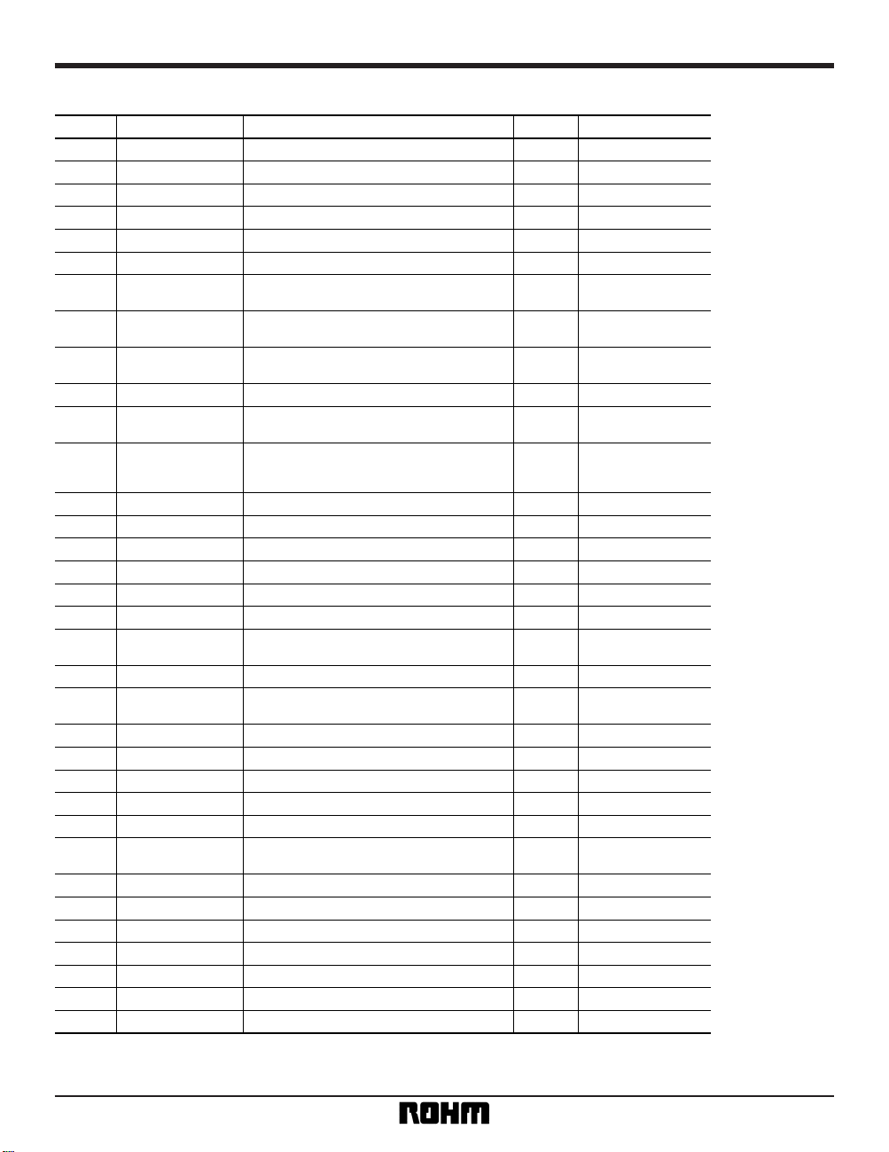
Pin descriptions
Pin No. Pin name I / O circuitPin voltageFunction
2, 1, 3 TUNER IN L, R, M 150kΩ0.0VTUNER input (L, R, M)
4 Hi-Fi ALC EF (NPN) ~ 200Ω0.0VALC time constant setting for Hi-Fi audio
5 SCL B (PNP)—CLOCK input for I2C BUS control
6 SDA B (PNP)—
—
DATA input for I2C BUS control
7 GNDD GND for I2C BUS control
8 FSC IN 200kΩ0.0V
9, 25 NR TC L, R —
—
—
– 5.0V
f
SC input for VCO and BPF adjustment
12, 22 DC FB L, R 11.5kΩ0.0VPNR operating reference potential point
15 GNDM —0.0VGND for PNR, MODEM and BPF
16 BPF f0 ADJ EF (NPN) ~ 200Ω1.9VCenter frequency adjustment for FM BPF
17 VCO f0 ADJ EF (NPN)2.5VVCO control current setting
18 VCCM —5.0VVCC for MODEM and BPF
19 FM ALC EF (NPN) ~ 2.5kΩ0.0VFM ALC time constant setting
20 AHSWP IN B (PNP)—Audio head switching pulse input
26 NORMAL IN 50kΩ0.0VNormal input
28 MIX OUT EF (NPN)0.0VMixer amplifier output for RF converter
30, 29 LINE L, R OUT 330Ω0.0VLine output
31 NORMAL OUT EF (P-P)0.0VNormal output
32 MUTE CTRL 3kΩ ( > 2.5V)—Line output mute control input
34, 33 LINE2 L, R IN 88kΩ0.0VLINE2 input (L, R)
36 VCC —5.0VVCC regulator
37 ERP C (NPN)5.0VVCC regulator error output
38 GND —0.0VI / O switch GND
39 VEE —
—
– 5.0VVEE regulator
41, 40 LINE1 IN L, R 88kΩ0.0VLINE1 input (L, R)
42 ERM C (PNP) – 5.0VVEE regulator error output
44, 43 BS IN L, R 88kΩ0.0VBS input (L, R)
PNR attack and recovery time setting.
Attack R: 530Ω, Recovery R: 6.5kΩ
10, 24 WTNG L, R 0.0V
Waiting characteristic, treble time constant
(External C = 0.022µF)
11, 23 NR EMPH L, R 0.0V
NR emphasis time constant setting
(External C = 0.0047µF)
13 FM PB IN 100kΩ0.0V
Playback FM input 660mV
P-P Typ.
Input coupling capacitor (GND ~ V
CC)
21 FM REC OUT EF (NPN) ~ 200ΩEE: 3.3V
EE: recording FM output, sine wave output
PB: FM BPF output monitor
27 MIX ALC EF (NPN) ~ 500Ω – 5.0V
ALC time constant setting for mixer amplifier.
Attack and recovery time setting
35 VREFP 10kΩ2.5V
V
CC / 2 reference voltage
(power on detect and pre-charge functions)
14 / ADJ FLAG
/ Hi-Fi DET
ENVE OUT
EE: 50kΩEE: 0.8V
PB, ADJ: EF (NPN)PB: 1.0V
FM Lch signal component envelope output
/ Hi-Fi DET output / ADJ FLAG output for ADJ
∗
I / O circuit; EF: emitter follower, P-P: push pull, B: base, and C: collector
All numerical values are standardized values.

4
Video ICs BH7801BK
•
Input / output circuits
TUNER L / R / M IN (2, 1, 3pin) LINE1, LINE2, BS L / R IN (34, 33, 41, 40, 44, 43pin)
LINE L / R OUT (30, 29pin) MIX OUT (28pin)
FM REC OUT (21pin) FM PB IN (13pin)
VCC
VEE
GND
1
3k
(2, 3pin)
– 2.0V
2.0V
150k
VCC
VEE
GND
33
58k
(34, 40, 41,
43, 44pin)
– 2.0V
2.0V
30k
VCC
VEE
GND
200
21
8k
200
VCC
VEE
GND
200
5k
47k
200
28
3P
VCC
VEE
GND
2k50k
13
12.5k
3.5V
100k
20P
PB
VCC
VEE
GND
25k 330
30
(29pin)
11.56k
26k
30k
50
50

5
Video ICs BH7801BK
AHSWP IN (20pin) ENVE OUT / ADJ FLAG / Hi-Fi DET (14pin)
SCL (5pin) SDA (6pin)
MUTE CTRL (32pin) FSC IN (8pin)
VCC
VEE
GND
20
5k
VCC
VEE
GND
14
50k
200
42.5k 30k
PB
VCC
VEE
5
30k
3V
VCC
VEE
GND
32
VCC
VEE
GND
2k
50k100k
100k
50k16k
200
10k
2.5V
51k
10k 2k
VCC
VEE
6
30k
90
3V
8
 Loading...