ROHM BD52E23G, BD52E24G, BD52E25G, BD52E26G, BD52E27G Schematic [ru]
...
Datasheet
2
22.May.2013 Rev.004
www.rohm.com
C
RL
RST
Micro
CT C
Micro
TOP VIEW
V
OUT
VDD
GND N.C. C
T
Voltage Detector IC Series
Free Delay Time Setting
CMOS Voltage Detector IC Series
BD52Exxx series BD53Exxx series
●General Description
Rohm's BD52Exxx and BD53Exxx series are highly
accurate, low current consumption Voltage Detector
ICs with a capacitor controlled time delay. The line up
includes BD52Exxx devices with N-channel open drain
output and BD53Exxx devices with CMOS output. The
devices are available for specific detection voltages
ranging from 2.3V to 6.0V in increments of 0.1V.
●Features
Delay Time Controlled by external Capacitor
Two output types (N-channel open drain and CMOS
output)
Ultra-low current consumption
Very small, lightweight and thin package
Package SSOP5 is similar to SOT-23-5(JEDEC)
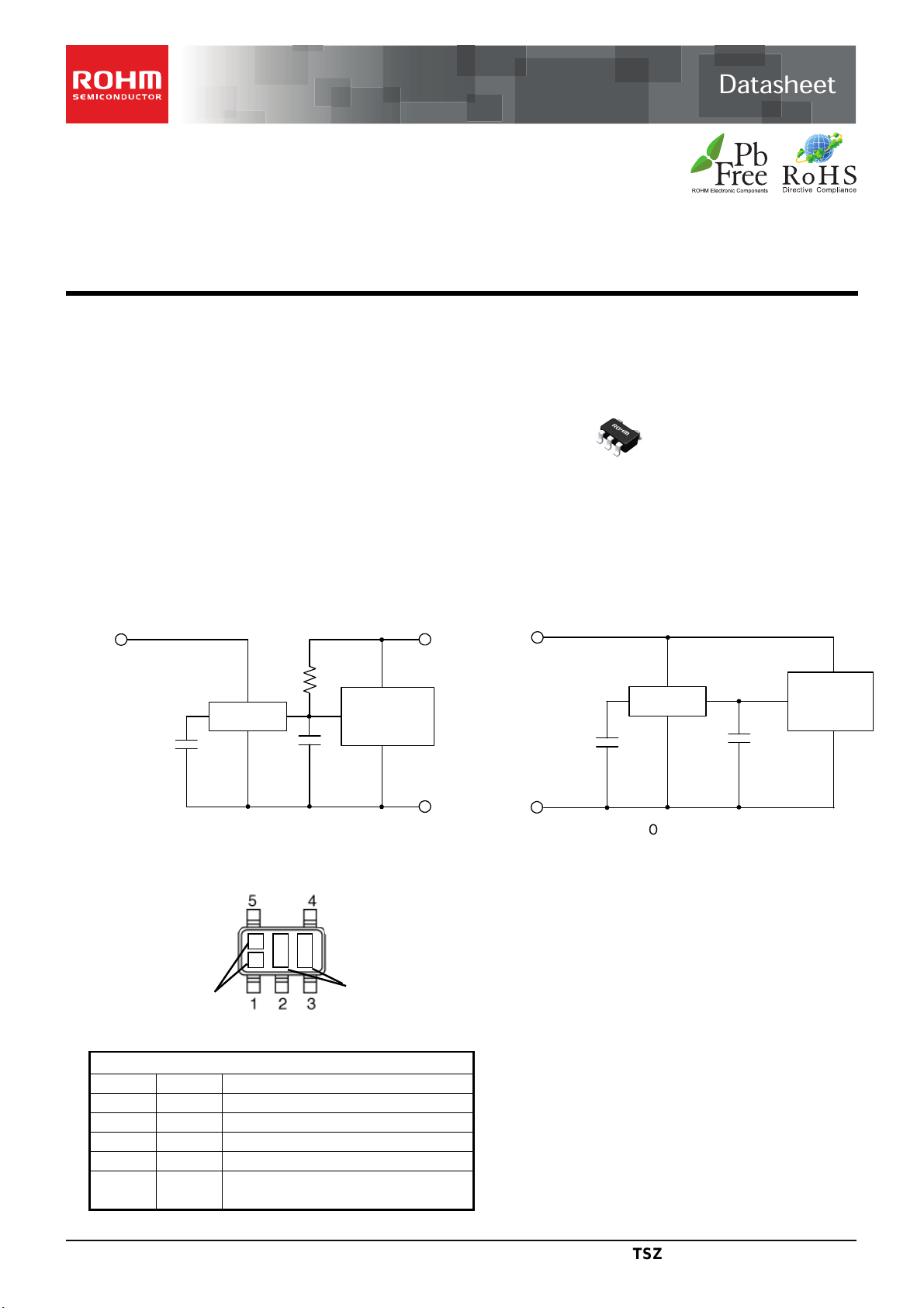
●Typical Application Circuit
V
DD1
V
C
T
BD52Exxx
Open Drain Output type
BD52Exxx Series
L
(Capacitor for
noise filtering)
controller
GND
●Connection Diagram
SSOP5
Marking
Lot. No
●Pin Descriptions
SSOP5
PIN No. Symbol Function
1 VOUT Reset Output
2 VDD Power Supply Voltage
3 GND GND
4 N.C. Unconnected Terminal
5 CT
Capacitor connection terminal for
output delay time
●Key Specifications
Detection voltage: 2.3V to 6.0V (Typ.)
0.1V steps
High accuracy detection voltage: ±1.0%
Ultra-low current consumption: 0.95µA (Typ.)
●Package
SSOP5: 2.90mm x 2.80mm x 1.25mm
●Applications
Circuits using microcontrollers or logic circuits that
require a reset.
DD2
VDD1
GND
BD53Exxx
CMOS Output type
BD53Exxx Series
(Capacitor for
noise filtering)
RST
controller
L
○Product structure:Silicon monolithic integrated circuit ○This product is not designed for protection against radioactive rays
.
© 2013 ROHM Co., Ltd. All rights reserved.
TSZ22111・14・001
1/12
TSZ02201-0R7R0G300080-1-

Datasheet
BD52Exxx series BD53Exxx series
2
22.May.2013 Rev.004
www.rohm.com
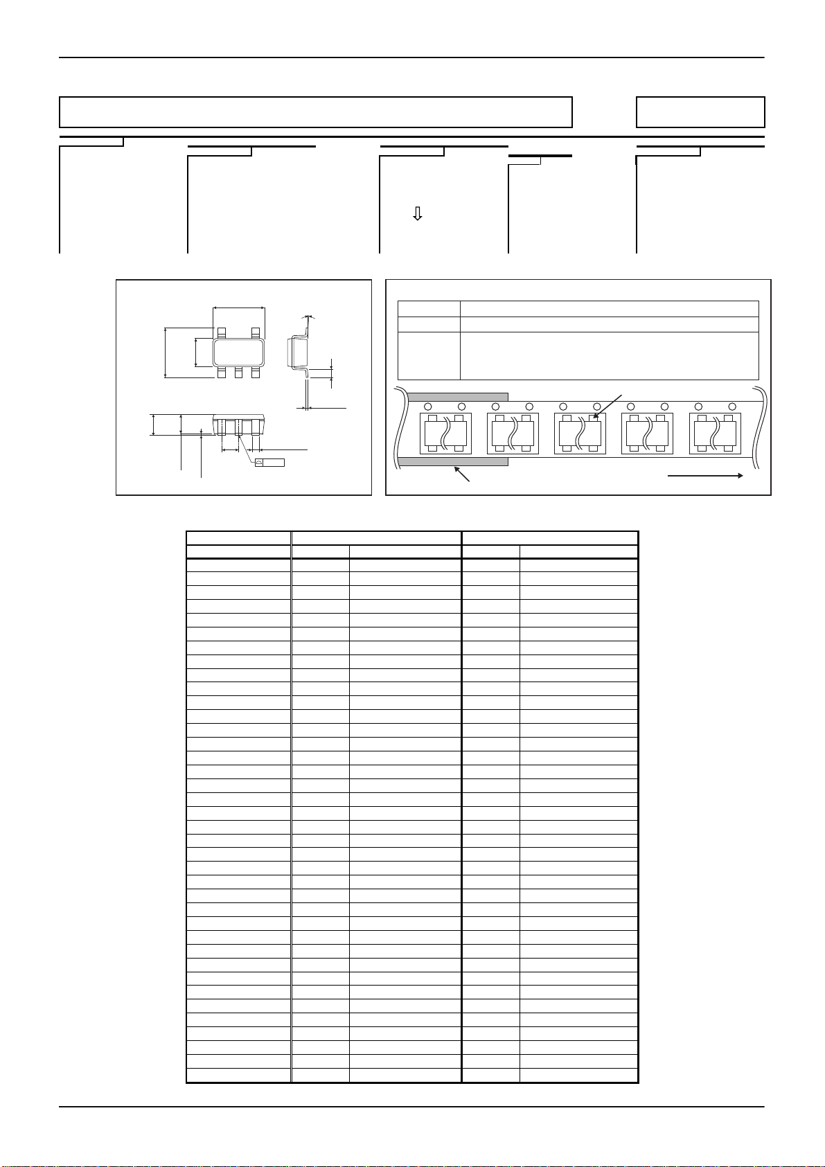
Output Type
Open Drain
CMOS
Detection
Voltage
Part Number
Part Number
6.0V
5.9V
Pg BD52E59
Uc
BD53E59
5.8V
Pf BD52E58
Ub
BD53E58
5.7V
Pe BD52E57
Ua
BD53E57
5.6V
Pd BD52E56
Ry
BD53E56
5.5V
Pc BD52E55
Rr
BD53E55
5.4V
Pb BD52E54
Rp
BD53E54
5.3V
Pa BD52E53
Rn
BD53E53
5.2V
Ny BD52E52
Rm
BD53E52
5.1V
Nr BD52E51
Rk
BD53E51
5.0V
Np BD52E50
Rh
BD53E50
4.9V
Nn BD52E49
Rg
BD53E49
4.8V
Nm BD52E48
Rf
BD53E48
4.7V
Nk BD52E47
Re
BD53E47
4.6V
Nh BD52E46
Rd
BD53E46
4.5V
Ng BD52E45
Rc
BD53E45
4.4V
Nf BD52E44
Rb
BD53E44
4.3V
Ne BD52E43
Ra
BD53E43
4.2V
Nd BD52E42
Qy
BD53E42
4.1V
Nc BD52E41
Qr
BD53E41
4.0V
Nb BD52E40
Qp
BD53E40
3.9V
Na BD52
E39 Qn BD53E39
3.8V
My BD52E38
Qm
BD53E38
3.7V
Mr BD52E37
Qk
BD53E37
3.6V
Mp BD52E36
Qh
BD53E36
3.5V
Mn BD52E35
Qg
BD53E35
3.4V
Mm BD52E34
Qf
BD53E34
3.3V
Mk BD52E33
Qe
BD53E33
3.2V
Mh BD52E32
Qd
BD53E32
3.1V
Mg BD52E31
Qc
BD53E31
3.0V
Mf BD52E30
Qb
BD53E30
2.9V
Me BD52E29
Qa
BD53E29
2.8V
Md BD52E28
Py
BD53E28
2.7V
Mc BD52E27
Pr
BD53E27
2.6V
Mb BD52E26
Pp
BD53E26
2.5V
Ma BD52E25
Pn
BD53E25
2.4V
Ly BD52E24
Pm
BD53E24
2.3V
Lr BD52E23
Pk
BD53E23
(Unit : mm)
SSOP5
2.9±0.2
0.13
4
°
+
6
°
−4
°
1.6
2.8±0.2
1.1±0.05
0.05±0.05
+0.2
−0.1
+0.05
−0.03
0.42
+0.05
−0.04
0.95
5
4
1 2
3
1.25Max.
0.2Min.
0.1
Direction of feed
Reel
∗
Order quantity needs to be multiple of the minimum quantity.
<Tape and Reel information>
Embossed carrier tapeTape
Quantity
Direction
of feed
The direction is the 1pin of product is at the upper right when you hold
reel on the left hand and you pull out the tape on the right hand
3000pcs
TR
( )
1pin
●Ordering Information
RE x x xB D x x - T
Part Output Type Reset Voltage Value Package Packaging and
Number 52 : Open Drain 23 : 2.3V G : SSOP5 forming specification
53 : CMOS 0.1V step TR : Embossed tape
60 : 6.0V and reel
●Lineup
© 2013 ROHM Co., Ltd. All rights reserved.
TSZ22111・15・001
2/12
TSZ02201-0R7R0G300080-1-

Datasheet
BD52Exxx series BD53Exxx series
2
22.May.2013 Rev.004
www.rohm.com
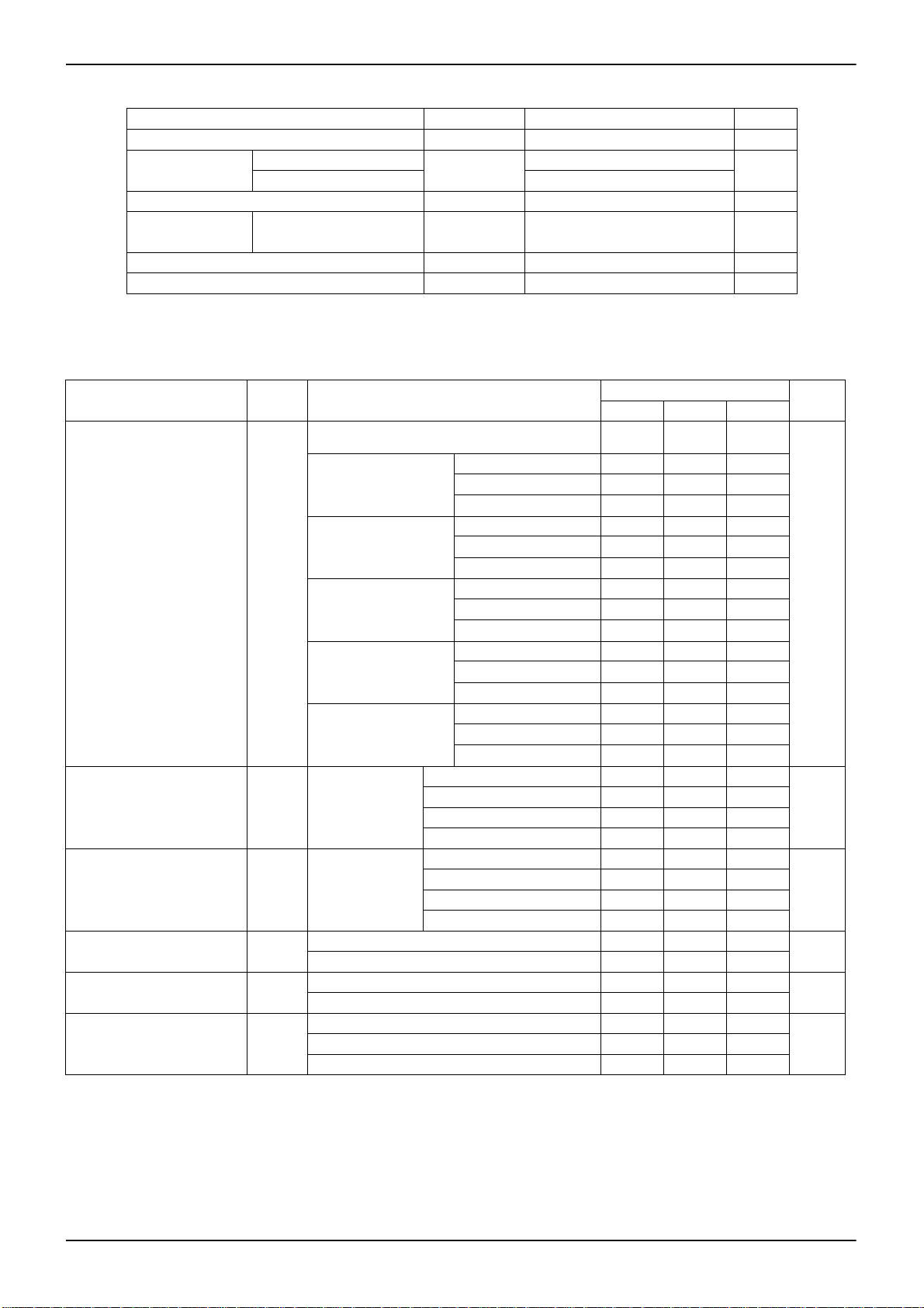
●Absolute maximum ratings
Parameter Symbol Limits Unit
Power Supply Voltage VDD-GND -0.3 to +10 V
Output Voltage
Nch Open Drain Output
CMOS Output GND-0.3 to VDD+0.3
V
OUT
Output Current Io 80 mA
Power
Dissipation
SSOP5
*1*2
Pd 540 mW
Operating Temperature Topr -40 to +105 °C
Ambient Storage Temperature Tstg -55 to +125 °C
*1 Reduced by 5.4mW/°C when used over 25°C.
*2 When mounted on ROHM standard circuit board (70mm×70mm×1.6mm, glass epoxy board).
●Electrical characteristics (Unless Otherwise Specified Ta=-40 to 105°C)
Parameter Symbol
VDD=HL, RL=470kΩ
Condition
*1
Ta=+25°C 2.475 2.5 2.525
VDET=2.5V
Ta=-40°C to 85°C
Ta=85°C to 105°C
Ta=+25°C 2.970 3.0 3.030
VDET=3.0V
Ta=-40°C to 85°C
Ta=85°C to 105°C
Detection Voltage V
DET
VDET=3.3V
Ta=+25°C 3.267 3.3 3.333
Ta=-40°C to 85°C
Ta=85°C to 105°C
Ta=+25°C 4.158 4.2 4.242
VDET=4.2V
Ta=-40°C to 85°C
Ta=85°C to 105°C
Ta=+25°C 4.752 4.8 4.848
VDET=4.8V
Ta=-40°C to 85°C
Ta=85°C to 105°C
V
=2.3-3.1V - 0.80 2.40
DET
V
=3.2-4.2V - 0.85 2.55
Circuit Current when ON IDD1 VDD=VDET-0.2V
Circuit Current when OFF IDD2 VDD=VDET+2.0V
Operating Voltage Range VOPL
‘Low’ Output Voltage (Nch) VOL
‘High’ Output Voltage (Pch) VOH
VOL≤0.4V, Ta=25 to 105°C, RL=470kΩ 0.95 - VOL≤0.4V, Ta=-40 to 25°C, RL=470kΩ 1.20 - VDD=1.5V, I
VDD=2.4V, I
VDD=4.8V, I
VDD=8.0V, I
SINK
= 0.4 mA, VDET=2.3-6.0V - - 0.5
SINK
= 2.0 mA, VDET=2.7-6.0V - - 0.5
SOURCE
SOURCE
SOURCE
DET
V
=4.3-5.2V - 0.90 2.70
DET
V
=5.3-6.0V - 0.95 2.85
DET
V
=2.3-3.1V - 0.75 2.25
DET
V
=3.2-4.2V - 0.80 2.40
DET
V
=4.3-5.2V - 0.85 2.55
DET
V
=5.3-6.0V - 0.90 2.70
DET
=0.7 mA, VDET(2.3V to 4.2V)
=0.9 mA, VDET(4.3V to 5.2V)
=1.1 mA, VDET(5.3V to 6.0V)
VDET (T) : Standard Detection Voltage (2.3V to 6.0V, 0.1V step)
RL: Pull-up resistor to be connected between VOUT and power supply.
Design Guarantee. (Outgoing inspection is not done on all products.)
*1 Guarantee is Ta=25°C.
GND-0.3 to +10
Limit
Min. Typ. Max.
VDET(T)
×0.99
VDET(T)
2.418 - 2.584
2.404 - 2.597
2.901 - 3.100
2.885 - 3.117
3.191 - 3.410
3.173 - 3.428
4.061 - 4.341
4.039 - 4.364
4.641 - 4.961
4.616 - 4.987
VDD-0.5
VDD-0.5
VDD-0.5
- -
- -
- -
V
Unit
VDET(T)
×1.01
V
µA
µA
V
V
V VDD=6.0V, I
© 2013 ROHM Co., Ltd. All rights reserved.
TSZ22111・15・001
3/12
TSZ02201-0R7R0G300080-1-

Datasheet
BD52Exxx series BD53Exxx series
2
22.May.2013 Rev.004
www.rohm.com
●Electrical characteristics (Unless Otherwise Specified Ta=-40 to 105°C) - continued
Parameter Symbol
Leak Current when OFF I
VDD=VDS=10V
leak
VDD=VDET×1.1, VDET=2.3-2.6V, RL=470kΩ
VDD=VDET×1.1, VDET=2.7-4.2V, RL=470kΩ
Condition
*1
- - 0.1 µA
×0.30
×0.30
CT pin Threshold Voltage VCTH
VDD=VDET×1.1, VDET=4.3-5.2V, RL=470kΩ
VDD=VDET×1.1, VDET=5.3-6.0V, RL=470kΩ
Output Delay Resistance RCT VDD=VDET×1.1 VCT=0.5V
CT pin Output Current ICT
Detection Voltage
Temperature coefficient
VDET/∆T Ta=-40°C to 105°C - ±100 ±360 ppm/°C
VCT=0.1V VDD=0.95V
VCT=0.5V VDD=1.5V 150 240 -
Hysteresis Voltage ∆ VDET VDD=LHL, RL=470kΩ
×0.35
×0.40
*1
5.5 9 12.5 MΩ
*1
15 40 -
VDET
×0.03
VDET (T) : Standard Detection Voltage (2.3V to 6.0V, 0.1V step)
RL: Pull-up resistor to be connected between VOUT and power supply.
Design Guarantee. (Outgoing inspection is not done on all products.)
*1 Guarantee is Ta=25°C.
Limit Unit
Min. Typ. Max.
VDD
VDD
VDD
VDD
VDD
×0.40
VDD
×0.45
VDD
×0.50
VDD
×0.50
VDET
×0.05
VDD
×0.60
VDD
×0.60
VDD
×0.60
VDD
×0.60
µA
VDET
×0.08
V
V
© 2013 ROHM Co., Ltd. All rights reserved.
TSZ22111・15・001
4/12
TSZ02201-0R7R0G300080-1-

Datasheet
BD52Exxx series BD53Exxx series
2
22.May.2013 Rev.004
www.rohm.com
V
V
V
V
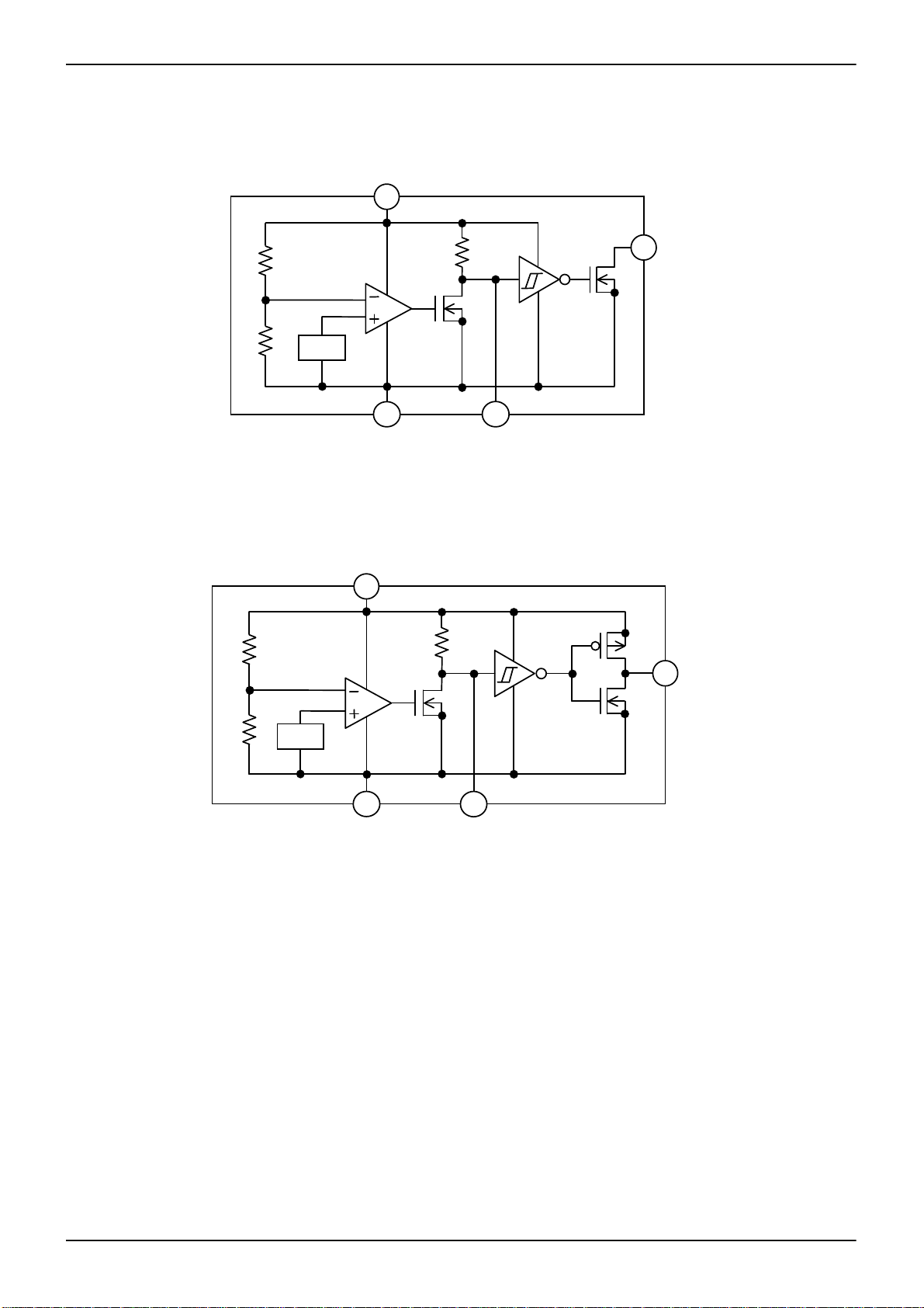
●Block Diagrams
Vref
Vref
DD
Figure.1 BD52Exxx Series
DD
Figure.2 BD53Exxx Series
GND
GND
OUT
CT
OUT
CT
© 2013 ROHM Co., Ltd. All rights reserved.
TSZ22111・15・001
5/12
TSZ02201-0R7R0G300080-1-
 Loading...