


查询BD45231G供应商
BD45XXXG
Voltage detectors
BD46XXXG
VOLTAGE DETECTOR IC
with counter timer
BD45XXXG
BD46XXXG
BD45XXXG and BD46XXXG are series of high-accuracy detection voltage and low current consumption
VOLTAGE DETECTOR ICs adopting CMOS process. New lineup of 156 types with delay time circuit
have developed. Delay time is fixed in the IC due to the built-in counter timer to require no external
capacitor. Total 156 types of VOLTAGE DETECTOR ICs including BD45XXXG series (Nch open drain
output) and BD46XXXG series (CMOS output), each of which has 26 kinds in every 0.1V step (2.3~4.8V)
and three kinds of delay time (50msec, 100msec, 200msec) have developed.
Applications
Every kind of appliances with microcontroller and logic circuit
Features
1) Built-in delay time circuit
(Fixed delay time by the built-in ±10% of high-accuracy counter timer)
2) No external capacitor for setting delay time required
3) 3 kinds of delay time: 50msec(Typ.)(BD45XX5G,BD46XX5G)
100msec(Typ.)(BD45XX1G,BD46XX1G)
200msec(Typ.)(BD45XX2G,BD46XX2G)
4) Detection voltage: 2.3V ~ 4.8V 0.1V step
5) High-accuracy detection voltage: ±1.0%
6) Ultra low current consumption: 0.85µA typ.
7) Output circuit: Nch open drain(BD45XXXG)
CMOS(BD46XXXG)
8) Package: SSOP5(SMP5C2)
9) Operating temperature range: -40°C ~ +105°C
BD45XXXG
BD46XXXG
1
2
2.9±0.2
(5)
0.2
0.1
0.2
–
+
±
1.6
2.8
±
1.1
1.25MAX
SSOP5(SMP5C2)
5
4
1pin : External RESET
control
2pin : Connect to
Sub, GND
3pin : GND
3
4pin : VOUT
5pin : VDD
(UNIT:mm)
(4)
0.2MIN
(2)(1)
(3)
0.05
0.95
0.05
±
0.05
0.42
0.1
0.13
+
–
0.05
0.04
+0.05
–0.03
Application Circuit
BD45XXXG BD46XXXG
VDD
Reset
Vout
1 2 3 4 5
ER Sub GND VOUT VDD
Vref
VDD
VDD
GND ER
Oscillation circuit
counter timer
Pin No.
SSOP5
Vref
VDD
VDD
GND
Oscillation circuit
counter timer
ER
Vout
Reset
1/4

Voltage detectors
Absolute Maximum Ratings (Ta=25˚C)
Parameter
Power supply voltage
Output
voltage
ER pin input voltage
Power dissipation:SSOP5
Operating temperature range
Storage temperature range
∗1 Derating: 5.4mW/˚C for operation above Ta=25˚C.(Mounted on a 70.0mmX70.0mmX16mm glass epoxy PCB.)
Nch open drain output
CMOS output
Symbol Unit
VDD – GND
VOUT
VCT
∗1
Pd
GND – 0.3 ~ VDD + 0.3
GND – 0.3 ~ VDD + 0.3
Topr
Tstg
Electrical characteristics (Unless otherwise noted; Ta=
Parameter
Detection voltage
temperature coefficient
Hysteresis voltage
Circuit current when ON
Circuit current when OFF
Min. operating voltage
"L" output current
"H" output current
Output leak current
"H" transmission
delay time
ER pin "H" voltage
ER pin "L" voltage
ER pin input current
∗1 This value is guranteed at Ta=25˚C.
Note) RL is not necessary for CMOS output type.
Note) Please refer to the detection voltage of Line-up table.
Symbol Min. Max. Unit ConditionsTyp.
∗1
VDET/∆T — ±100 ±360 ppm/˚C
VDETX0.03
∗1
Icc1
— 0.70 2.10 VDET=2.3~3.1V
— 0.75 2.25
—
∗1
Icc2
— 0.75 VDET=2.3~3.1V2.25
—
—
0.95 — — VVOPL RL=470kΩ, VOL≥0.4V
0.4 1.2 — VDS=0.5V, VDD=1.2V
2.0 5 —
∗1
IOH
∗1
Ilaek
∗1
tPLH
1.0 2.2
1.2 2.7 —
—
45 50 55
90 100 110
180 200 220
∗1
VEH
∗1
2.0 — —
— — 0.8VEL
— 1 10IER
Limits
– 0.3 ~ + 10
GND – 0.3 ~ + 10
540
– 40 ~ + 105
– 55 ~ + 125
-
25˚C ~ +105˚C)
VDETX0.05
VDETX0.08
0.80
0.80
0.85
—
2.40
2.40
2.55
—
0.1
V
V
V
mW
˚C
˚C
%∆VDET
µA
µA
mAIOL
mA
µA
V
V
V
µA
BD45XXXG
BD46XXXG
Ta=-40˚C ~ +105˚C
RL=470KΩ, VDD=L→H→L
VDD=VDET–0.2V
VDD=VDET+2V
VDS=0.5V, VDD=2.4V (VDET≥2.7V)
VDS=0.5V, VDD=4.8V
VDS=0.5V, VDD=6.0V VDET=4.3~4.8V
VDD=VDS=10V
RL=100kΩ
CL=100pF
VER=2.0V
VDET=3.2~4.2V
VDET=4.3~4.8V
VDET=3.2~4.2V
VDET=4.3~4.8V
VDET=2.3~4.2V
BD45XX5G, BD46XX5G
BD45XX1G, BD46XX1G
BD45XX2G, BD46XX2G
Characteristic diagram and Measurement circuit
250
(BD4x28xG tPLH)
200
150
100
tPLH (msec)
50
0
-60-40-
VDET±0.5V
Output delay time "L → H"
BD45282G
BD45281G
BD45285G
20 20 40 60 80 100 120
0
Ta (°C)
5V
VDD
VOUTER
GND
RL=100kΩ
100pF
50
40
30
20
tPLH [µsec]
10
-60-40-
VDET±0.5V
0
Output delay time "H → L"
(BD4x28x tPLH)
20 20 40 60 80 100 120
0
Ta (°C)
5V
RL=100kΩ
100pF
ER
VDD
VOUT
GND
2/4

3/4
Voltage detectors
BD45XXXG
BD46XXXG
521 43 1076 98
0.5
1.0
1.5
VDD
(V)
I
DD
(µA)
0
(BD45281G)
3.50.5 1.5 2.5 3 4.54 5.5521
1
2
3
4
5
6
7
8
9
0
VDD
(V)
VOUT
(V)
Ta=25˚C
Ta=25˚C
(BD45421G)
18
(mA)
1.5 2 2.5
10
15
0.5 1
5
0
VDS
(V)
IOL
VDD=1.2V
VDD=2.4V
(BD45281G)
Timing waveform
VDD
VDD
VOUTER
GND
A
VDD
VDS
VDD
VOUT
GND
A
0 50–40 90
Ta
(˚C)
3.4
3.8
4.2
4.6
5.0
5.4
VDET
(V)
(BD45421G)
low to high(V
DET
+∆V
DET
)
high to low(V
DET
)
VDD
VDS
VDD
VOUT
GND
A
ER ER
RL=470KΩ
VDD
V
VDD
VOUT
GND
ER
RL=470KΩ
VDD
V
VDD
VOUT
GND
ER
3 4 5 6
10
15
1 2
2
5
0
VDS
(V)
IDS
(mA)
V
DD
=4.8V
V
DD
=6
.0V
(BD46281G)
tPLH tPLH
tPHL tPHL
tPLH
VDD
VDD
VOUT
ER
VDET
0V
VOH
VOL
VEH
VDET+∆VDET
Circuit current "L" output current "H" output current
I/O characteristic Detection voltage
Voltage detectors
Part number and Marking of samples
MarkingVoltage Part No.
T0
4.8V
4.7V
T1
4.6V
T2
4.5V
T3
4.4V
T4
T5
4.3V
4.2V
T6
4.1V
T7
4.0V
T8
3.9V
T9
3.8V
TA
3.7V
TB
3.6V
TC
3.5V
TD
3.4V
TE
3.3V
TF
3.2V
TG
3.1V
TH
3.0V
TJ
TK
2.9V
2.8V
TL
TM
2.7V
2.6V
TN
2.5V
TP
2.4V
TQ
TR
2.3V BD45235
Marking Part No. Marking Part No. Marking Part No.
BD45485
BD45475
BD45465
BD45455
BD45445
BD45435
BD45425
BD45415
BD45405
BD45395
BD45385
BD45375
BD45365
BD45355
BD45345
BD45335
BD45325
BD45315
BD45305
BD45295
BD45285
BD45275
BD45265
BD45255
BD45245
TS
TT
TU
TV
TW
TX
TY
TZ
U0
U1
U2
U3
U4
U5
U6
U7
U8
U9
UA
UB
UC
UD
UE
UF
UG
UH
BD45481
BD45471
BD45461
BD45451
BD45441
BD45431
BD45421
BD45411
BD45401
BD45391
BD45381
BD45371
BD45361
BD45351
BD45341
BD45331
BD45321
BD45311
BD45301
BD45291
BD45281
BD45271
BD45261
BD45251
BD45241
BD45231
UM
UN
UP
UQ
UR
US
UT
UU
UV
UW
UX
UY
UZ
UJ
BD45482
UK
BD45472
BD45462
UL
BD45452
BD45442
BD45432
BD45422
BD45412
BD45402
BD45392
BD45382
BD45372
BD45362
BD45352
BD45342
BD45332
BD45322
V0
BD45312
V1
BD45302
V2
V3
BD45292
BD45282
V4
V5
BD45272
BD45262
V6
BD45252
V7
BD45242
V8
V9
BD45232
VC
VD
VG
VH
VM
VN
VQ
VR
VU
VW
W0
W1
BD45XXXG
BD46XXXG
Marking
BD46485
VA
VB
BD46475
BD46465
BD46455
BD46445
VE
BD46435
VF
BD46425
BD46415
BD46405
VJ
BD46395
VK
BD46385
VL
BD46375
BD46365
BD46355
VP
BD46345
BD46335
BD46325
VS
BD46315
VT
BD46305
VV
BD46295
BD46285
VX
BD46275
BD46265
VY
BD46255
VZ
BD46245
W2
W3
W4
W5
W6
W7
W8
W9
WA
WB
WC
WD
WE
WF
WG
WH
WJ
WK
WL
WM
WN
WP
WQ
WR
WS
WT
Part No.
BD46481
BD46471
BD46461
BD46451
BD46441
BD46431
BD46421
BD46411
BD46401
BD46391
BD46381
BD46371
BD46361
BD46351
BD46341
BD46331
BD46321
BD46311
BD46301
BD46291
BD46281
BD46271
BD46261
BD46251
BD46241
BD46231
Marking
WU
WV
WW
WX
WY
WZ
X0
X1
X2
X3
X4
X5
X6
X7
X8
X9
XA
XB
XC
XD
XE
XF
XG
XH
XJ
XKBD46235
Part No.
BD46482
BD46472
BD46462
BD46452
BD46442
BD46432
BD46422
BD46412
BD46402
BD46392
BD46382
BD46372
BD46362
BD46352
BD46342
BD46332
BD46322
BD46312
BD46302
BD46292
BD46282
BD46272
BD46262
BD46252
BD46242
BD46232
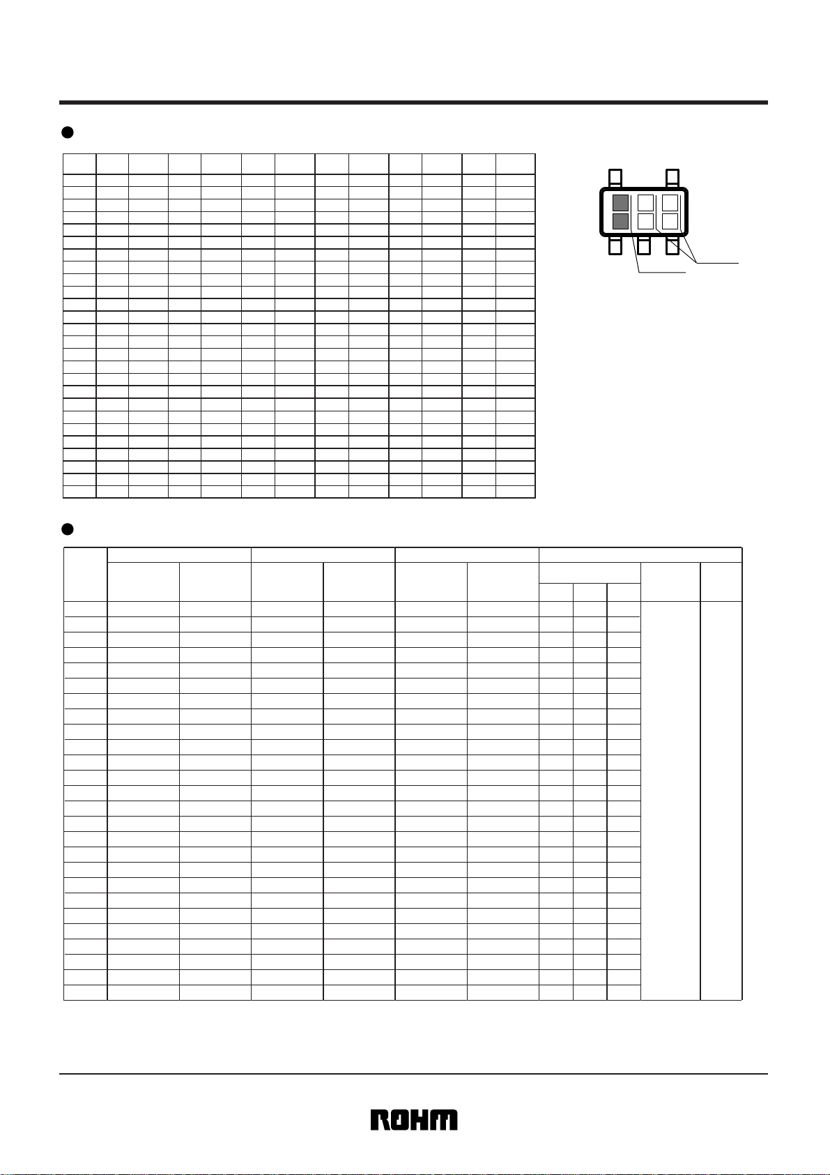
BD45XXXG/BD46XXXG : SSOP5(SMP5C2)
(5)
(1)
(2)
Marking
(4)
(3)
Lot.No
Line-up
Detection
voltage
VDET
4.8V
4.7V
4.6V
4.5V
4.4V
4.3V
4.2V
4.1V
4.0V
3.9V
3.8V
3.7V
3.6V
3.5V
3.4V
3.3V
3.2V
3.1V
3.0V
2.9V
2.8V
2.7V
2.6V
2.5V
2.4V
2.3V
Nch
open drain output
BD45485G
BD45475G
BD45465G
BD45455G
BD45445G
BD45435G
BD45425G
BD45415G
BD45405G
BD45395G
BD45385G
BD45375G
BD45365G
BD45355G
BD45345G
BD45335G
BD45325G
BD45315G
BD45305G
BD45295G
BD45285G
BD45275G
BD45265G
BD45255G
BD45245G
BD45235G
50msec delay
CMOS output
BD46485G
BD46475G
BD46465G
BD46455G
BD46445G
BD46435G
BD46425G
BD46415G
BD46405G
BD46395G
BD46385G
BD46375G
BD46365G
BD46355G
BD46345G
BD46335G
BD46325G
BD46315G
BD46305G
BD46295G
BD46285G
BD46275G
BD46265G
BD46255G
BD46245G
BD46235G
100msec delay
Nch
open drain output
CMOS output
BD45481G
BD45471G
BD45461G
BD45451G
BD45441G
BD45431G
BD45421G
BD45411G
BD45401G
BD45391G
BD45381G
BD45371G
BD45361G
BD45351G
BD45341G
BD45331G
BD45321G
BD45311G
BD45301G
BD45291G
BD45281G
BD45271G
BD45261G
BD45251G
BD45241G
BD45231G
BD46481G
BD46471G
BD46461G
BD46451G
BD46441G
BD46431G
BD46421G
BD46411G
BD46401G
BD46391G
BD46381G
BD46371G
BD46361G
BD46351G
BD46341G
BD46331G
BD46321G
BD46311G
BD46301G
BD46291G
BD46281G
BD46271G
BD46261G
BD46251G
BD46241G
BD46231G
200msec delay
Nch
open drain output
CMOS output
BD45482G
BD45472G
BD45462G
BD45452G
BD45442G
BD45432G
BD45422G
BD45412G
BD45402G
BD45392G
BD45382G
BD45372G
BD45362G
BD45352G
BD45342G
BD45332G
BD45322G
BD45312G
BD45302G
BD45292G
BD45282G
BD45272G
BD45262G
BD45252G
BD45242G
BD45232G
BD46482G
BD46472G
BD46462G
BD46452G
BD46442G
BD46432G
BD46422G
BD46412G
BD46402G
BD46392G
BD46382G
BD46372G
BD46362G
BD46352G
BD46342G
BD46332G
BD46322G
BD46312G
BD46302G
BD46292G
BD46282G
BD46272G
BD46262G
BD46252G
BD46242G
BD46232G
Detection voltage
VDET ( V )Ta=25˚C
Min.
Typ.
4.752
4.800
4.653
4.700
4.554
4.600
4.455
4.500
4.356
4.400
4.257
4.300
4.158
4.200
4.059
4.100
3.960
4.000
3.861
3.900
3.762
3.800
3.663
3.700
3.564
3.600
3.465
3.500
3.366
3.400
3.267
3.300
3.168
3.200
3.069
3.100
2.970
3.000
2.871
2.900
2.772
2.800
2.673
2.700
2.574
2.600
2.475
2.500
2.376
2.400
2.277
2.300
Max.
4.848
4.747
4.646
4.545
4.444
4.343
4.242
4.141
4.040
3.939
3.838
3.737
3.636
3.535
3.434
3.333
3.232
3.131
3.030
2.929
2.828
2.727
2.626
2.525
2.424
2.323
Hysteresis
voltage
( V, Typ. )
V
DET
X 0.05
Package
SSOP5
(SMP5C2)
4/4
 Loading...