

Datasheet
Voltage Detector IC Series
Counter Timer Built-in
CMOS Voltage Detector IC
BD45xxx series BD46xxx series
●General Description
ROHM’s BD45xxx and BD46xxx series are highly
accurate, low current consumption reset IC series.
Because the counter timer delay circuit is built into
those series, an external capacitor for the delay time
setting is unnecessary. The lineup was established
with tow output types (Nch open drain and CMOS
output) and detection voltages range from 2.3V to 4.8V
in increments of 0.1V, so that the series may be
selected according the application at hand.
●Features
Counter Timer Built-in
None delay time setting capacitor
Ultra-low current consumption
Tow output types (Nch open drain and CMOS output)
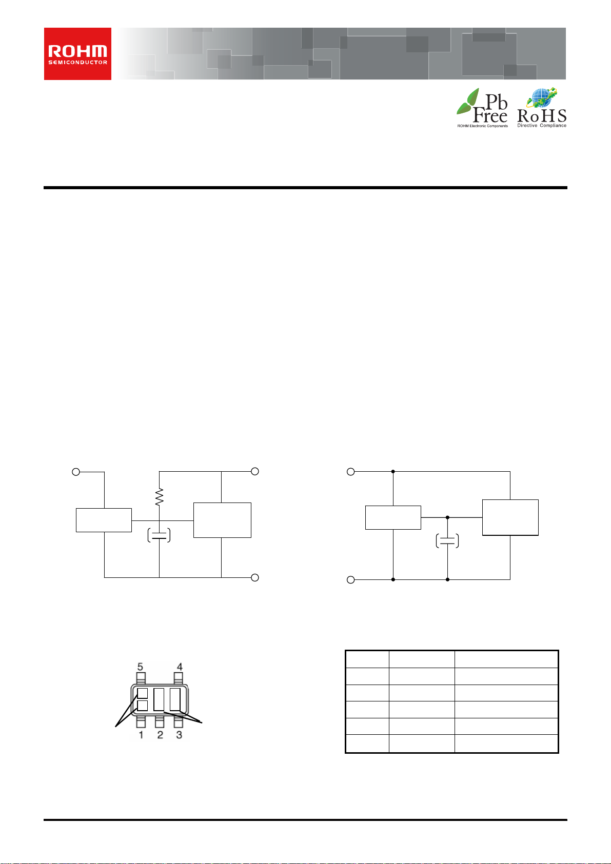
●Ty pical A pplication Circuit
VDD1 VDD2
BD45xxx
(Open Drain Output Type)
●Connection Diagram
SSOP5
Marking
ER SUB GND
○Product structure:Silicon monolithic integrated circuit ○This product is not designed protection against radioactive rays.
R
L
RST
CL
(Noise-filtering
Capacitor)
BD45xxx series
OUT VDD
V
TOP VIEW
Lot. No
Micro
controller
GND
●Key Specifications
Detection voltage: 2.3V to 4.8V (Typ.)
High accuracy detection voltage: ±1.0%
Ultra-low current consumption: 0.85µA (Typ.)
Operating temperature range: -40°C to +105°C
Three internal, fixed delay time: 50ms
100ms
200ms
●Package
SSOP5 2.90mm x 2.80mm x 1.15mm
●Applications
All electronic devices that use microcontrollers
and logic circuits
VDD1
GND
BD46xxx
CL
(Noise-filterin g
Capacitor)
RST
(CMOS Output Type)
BD46xxx series
●Pin Descriptions
PIN No. Symbol Function
1 ER Manual Reset
2 SUB Substrate *
3 GND GND
4 VOUT Reset Output
5 VDD Power Supply Voltage
*Connect the substrate to GND.
0.1V steps
Micro
controller
www.rohm.com © 2011 ROHM Co., Ltd. All rights reserved.
TSZ22111・14・001
1/10
TSZ02201-0R7R0G300010-1-2
19.DEC.2011 Rev.002
BD45xxx series BD46xxx series
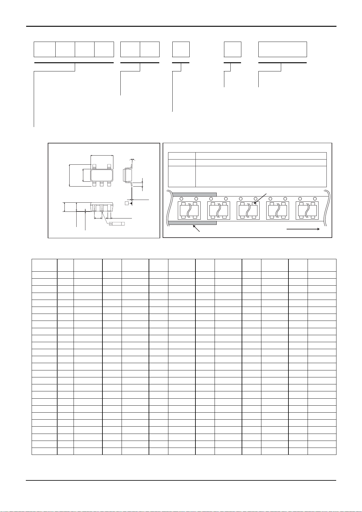
●Ordering Information
Datasheet
B D 4 5
BD45: Reset Voltage Value
Open Drain Type
CMOS Detector IC with
Built-In Counter Timer
1: 100ms
CMOS Detector IC with
Built-In Counter Timer
2 3 1 G - T R
Counter Timer
23: 2.3V
48: 4.8V 5: 50ms
Delay Time Settings
2: 200ms BD46: CMOS Output Type
Package
G:SSOP5
Packaging and forming specification
TR: Embossed tape and reel
SSOP5
<Tape and Reel information>
Embossed carrier tapeTape
Quantity
Direction
of feed
3000pcs
TR
The direction is the 1pin of product is at the upper right when you hold
()
reel on the left hand and you pull out the tape on the right hand
Reel
1pin
Direction of feed
Order quantity needs to be multiple of the minimum quantity.
∗
2.8±0.2
1.25Max.
1.1±0.05
°
+0.05
−0.04
S
+
6
°
4
°
−4
+0.05
0.13
−0.03
(Unit : mm)
0.2Min.
2.9±0.2
5
4
+0.2
−0.1
1.6
12
3
0.95
0.05±0.05
0.42
0.1 S
●Lineup
Detection
Voltage
Mar
king
Part
Number
Mark
ing
Part
Number
Mark
ing
Part
Number
Mark
ing
Part
Number
Mark
ing
Part
Number
Mark
ing
4.8V T0 BD45485 TS BD45481 UJ BD45482 VA BD46485 W2 BD46481 WU BD46482
4.7V T1 BD45475 TT BD45471 UK BD45472 VB BD46475 W3 BD46471 WV BD46472
4.6V T2 BD45465 TU BD45461 UL BD45462 VC BD46465 W4 BD46461 WW BD46462
4.5V T3 BD45455 TV BD45451 UM BD45452 VD BD46455 W5 BD46451 WX BD46452
4.4V T4 BD45445 TW BD45441 UN BD45442 VE BD46445 W6 BD46441 WY BD46442
4.3V T5 BD45435 TX BD45431 UP BD45432 VF BD46435 W7 BD46431 WZ BD46432
4.2V T6 BD45425 TY BD45421 UQ BD45422 VG BD46425 W8 BD46421 X0 BD46422
4.1V T7 BD45415 TZ BD45411 UR BD45412 VH BD46415 W9 BD46411 X1 BD46412
4.0V T8 BD45405 U0 BD45401 US BD45402 VJ BD46405 WA BD46401 X2 BD46402
3.9V T9 BD45395 U1 BD45391 UT BD45392 VK BD46395 WB BD46391 X3 BD46392
3.8V TA BD45385 U2 BD45381 UU BD45382 VL BD46385 WC BD46381 X4 BD46382
3.7V TB BD45375 U3 BD45371 UV BD45372 VM BD46375 WD BD46371 X5 BD46372
3.6V TC BD45365 U4 BD45361 UW BD45362 VN BD46365 WE BD46361 X6 BD46362
3.5V TD BD45355 U5 BD45351 UX BD45352 VP BD46355 WF BD46351 X7 BD46352
3.4V TE BD45345 U6 BD45341 UY BD45342 VQ BD46345 WG BD46341 X8 BD46342
3.3V TF BD45335 U7 BD45331 UZ BD45332 VR BD46335 WH BD46331 X9 BD46332
3.2V TG BD45325 U8 BD45321 V0 BD45322 VS BD46325 WJ BD46321 XA BD46322
3.1V TH BD45315 U9 BD45311 V1 BD45312 VT BD46315 WK BD46311 XB BD46312
3.0V TJ BD45305 UA BD45301 V2 BD45302 VU BD46305 WL BD46301 XC BD46302
2.9V TK BD45295 UB BD45291 V3 BD45292 VV BD46295 WM BD46291 XD BD46292
2.8V TL BD45285 UC BD45281 V4 BD45282 VW BD46285 WN BD46281 XE BD46282
2.7V TM BD45275 UD BD45271 V5 BD45272 VX BD46275 WP BD46271 XF BD46272
2.6V TN BD45265 UE BD45261 V6 BD45262 VY BD46265 WQ BD46261 XG BD46262
2.5V TP BD45255 UF BD45251 V7 BD45252 VZ BD46255 WR BD46251 XH BD46252
2.4V TQ BD45245 UG BD45241 V8 BD45242 W0 BD46245 WS BD46241 XJ BD46242
2.3V TR BD45235 UH BD45231 V9 BD45232 W1 BD46235 WT BD46231 XK BD46232
Part
Number
www.rohm.com © 2011 ROHM Co., Ltd. All rights reserved.
TSZ22111・15・001
2/10
TSZ02201-0R7R0G300010-1-2
19.DEC.2011 Rev.002
BD45xxx series BD46xxx series
z Absolute maximum ratings (Ta=25°C)
Parameter Symbol Limits Unit
Power Supply Voltage VDD-GND -0.3 to +10 V
Output Voltage
Nch Open Drain Output GND-0.3 to +10
CMOS Output
VOUT
GND-0.3 to V
DD
+0.3
V
ER pin Voltage VCT GND-0.3 to VDD+0.3 V
Power Dissipation
*1 *2
Pd 540 mW
Operating Temperature Topr -40 to +105 °C
Ambient Storage Temperature Tstg -55 to +125 °C
*1 Use above Ta=25°C results in a 5.4mW loss per degree.
*2 When mounted on a 70mm×70mm×1.6mm glass epoxy board.
●Electrical characteristics (Unless Otherwise Specified Ta=-40 to 105°C)
Parameter Symbol Condition
Detection Voltage VDET VDD=HÆL, RL=470kΩ
Detection Voltage
Temperature coefficient
Hysteresis Voltage ∆VDET
‘High’ Output
Delay time
Circuit Current
when ON
Circuit Current
when OFF
Operating Voltage Range VOPL
‘High’ Output Current
‘Low’Output Current (Nch)
Leak Current when OFF I
V
DET/
∆T
tPLH
I
DD1
I
DD2
I
I
-40°C to +105°C
VDD=LÆHÆL, RL=470kΩ
CL=100pF,
RL=100kΩ
VDD=VDET-0.2V, VER=0V VDET=2.3V to 3.1V *1 - 0.70 2.10
VDD=VDET-0.2V, VER=0V VDET=2.3V to 3.1V
VDD=VDET-0.2V, VER=0V VDET=3.2V to 4.2V *1 - 0.75 2.25
VDD=VDET-0.2V, VER=0V VDET=3.2V to 4.2V
VDD=VDET-0.2V, VER=0V VDET=4.3V to 4.8V *1 - 0.80 2.40
VDD=VDET-0.2V, VER=0V VDET=4.3V to 4.8V
VDD=VDET+0.2V, VER=0V VDET=2.3V to 3.1V
VDD=VDET+0.2V, VER=0V VDET=2.3V to 3.1V
VDD=VDET+0.2V, VER=0V VDET=3.2V to 4.2V
VDD=VDET+0.2V, VER=0V VDET=3.2V to 4.2V
VDD=VDET+0.2V, VER=0V VDET=4.3V to 4.8V
VDD=VDET+0.2V, VER=0V VDET=4.3V to 4.8V
VOL≤0.4V, RL=470kΩ, Ta=25 to 105°C
VOL≤0.4V, RL=470kΩ, Ta=-40 to 25°C
OH
VDS=0.5V,VDD=6.0V,VDET≥4.3V
VDS=0.5V, VDD=1.2V
OL
VDS=0.5V, VDD=2.4V VDET=2.7V to 4.8V
VDD=VDS=10V
leak
*1, *2, *3
BD45XX5, BD46XX5
BD45XX1, BD46XX1
BD45XX2, BD46XX2
ER Pin ‘H’ Voltage VEH
ER Pin ‘L’ Voltage VEL
ER Pin Input Current IEL
VDET(T):Standard Detection Voltage (2.3V to 4.8V, 0.1V step)
R
L :Pull-up resistor to be connected between VOUT and power supply.
C
L :Capacitor to be connected between VOUT and GND.
*1 Guarantee is Ta=25°C.
*2
tPLH:VDD=(VDET(T)-0.5V)Æ(VDET(T)+0.5V)
*3
tPLH:VDD=Please set up the rise up time between VDD=0ÆVDET more than 100µs.
Attention: Please connect the GND when you don’t use ‘ER’
Min. Typ. Max.
VDET(T)
*1
×0.99
- ±100 ±360 ppm/°C
VDET(T)
×0.03
45 50 55
90 100 110
180 200 220
- 0.70 2.85
- 0.75 3.00
*1
*1
*1
- 0.80 3.15
- 0.75 2.25
- 0.75 4.28
- 0.80 2.40
- 0.80 4.50
- 0.85 2.55
- 0.85 4.73
0.95 - -
1.20 - -
1.2 2.7 - mA
0.4 1.2 -
*1
2.0 5.0 -
- - 0.1 µA
*1
2.0 - - V
*1
- - 0.8 V
- 1 10 µA
Limit
V
DET(T)
DET(T)
V
×0.05
V
DET(T)
×1.01
DET(T)
V
×0.08
Datasheet
Unit
V
V
ms
µA
µA
V
mA
www.rohm.com © 2011 ROHM Co., Ltd. All rights reserved.
TSZ22111・15・001
3/10
TSZ02201-0R7R0G300010-1-2
19.DEC.2011 Rev.002
BD45xxx series BD46xxx series
R
R
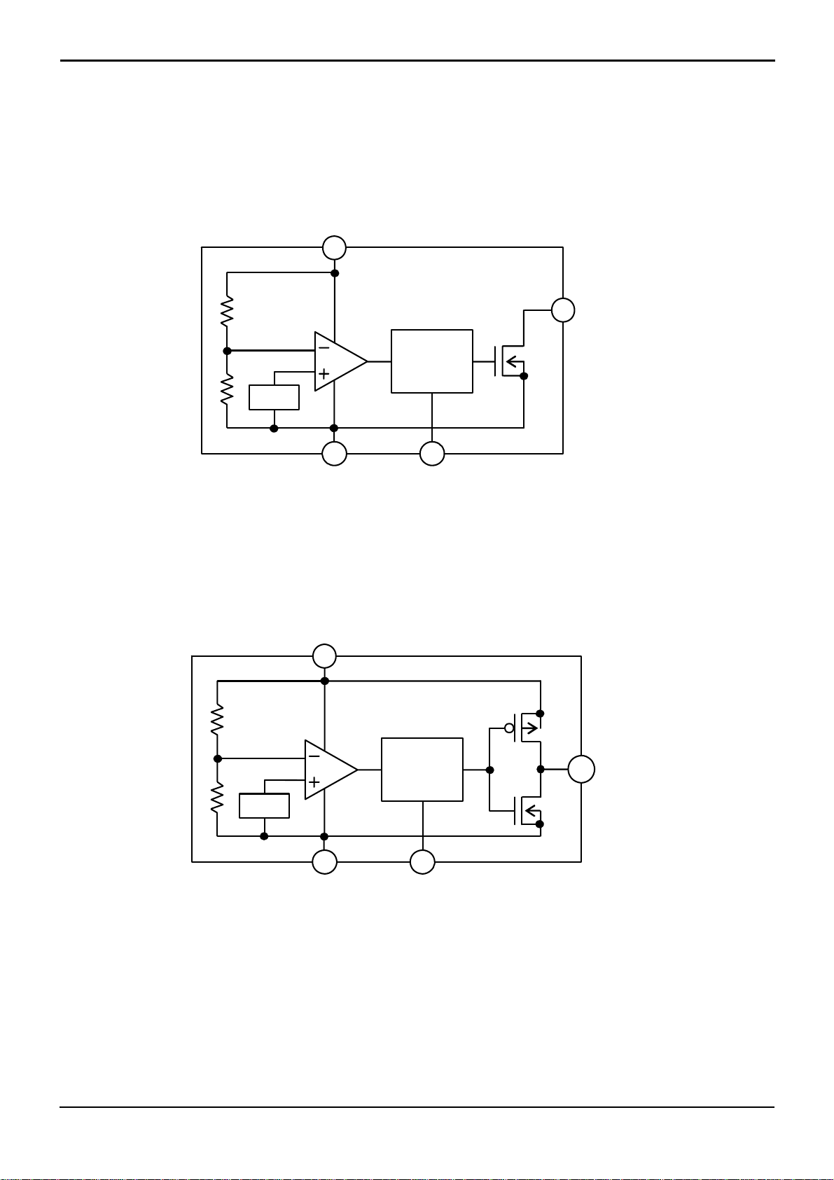
●Block Diagrams
Vref
GND
Fig.1 BD45xxx Series
VDD
Vref
VDD
Oscillation
Circuit Counter
Timer
E
Oscillation
Circuit Counter
Timer
Datasheet
VOUT
VOUT
GND
Fig.2 BD46xxx Series
www.rohm.com © 2011 ROHM Co., Ltd. All rights reserved.
TSZ22111・15・001
4/10
E
TSZ02201-0R7R0G300010-1-2
19.DEC.2011 Rev.002

BD45xxx series BD46xxx series
●Typical Performance Curves
DD
:
[μA]
I
2.0
1.5
BD45281G
【BD45281】
【
【BD46281】
1.0
0.5
CIRCUIT CURRENT
0.0
01 23 45678 910
V
SUPPLY VOLTAGE :VDD[V]
DD
Fig.3 Circuit Current
[mA]
OH
I
:
20
15
BD46281G
【
【BD46281】
VDD=6.0V
10
VDD=4.8V
5
0
"HIGH" OUTPUT CURRENT
0123456
DRAIN-SOURCE VOLTAGE : V
Fig.5 “High” Output Current
】
DS
】
[V]
20
【BD45281】
BD 45281G
[mA]
OL
I
:
15
10
5
0
"LOW" OUTPUT CURRENT
0.0 0.5 1.0 1.5 2.0 2.5
DRAIN-SOU R C E VOLTAGE : V
【
【BD46281】
Fig.4 “Low” Output Current
7
BD45421G
【BD45281】
[V]
OUT
V
:
6
5
【
【BD46281】
4
3
Ta=25
2
1
OUTPUT VOLTAGE
Ta=25
℃
0
00.511.522.5 33.544.5 55.5
VDD SUPPLY VOLTAGE :VDD[V]
Fig.6 I/O Characteristics
Datasheet
VDD=2.4V
VDD=1.2V
℃
DS
】
】
[V]
www.rohm.com © 2011 ROHM Co., Ltd. All rights reserved.
TSZ22111・15・001
5/10
TSZ02201-0R7R0G300010-1-2
19.DEC.2011 Rev.002

BD45xxx series BD46xxx series
[V]
OUT
V
:
20
15
【BD45281】
BD46281G
【
【BD46281】
10
5
OUTPUT VOLTAGE
0
01234 5678910
ER VOLTAGE : VER[V]
Fig.7 ER Terminal Threshold Voltage
:
[V]
DET
V
5.8
5.4
5.0
4.6
4.2
BD 45421G
【BD45421】【BD46421】
Low to hig h( V
【
DET
+ ΔV
DET
3.8
3.4
DETECTION VOLTAGE
3.0
-40 0 40 80
~
TEMPERATURE : Ta[℃]
Fig.9 Detection Voltage
High to low(V
Release Voltage
DET
Datasheet
20
BD 45421G
【
】
[μA]
15
ER
I
:
【BD45421】
【BD46421】
10
5
ER BIAS CURRENT
0
012345678910
ER VOLTAGE : V
[V]
ER
Fig.8 ER Terminal Input Current
1.6
】
)
)
[μA]
1.4
DD1
I
:
1.2
1.0
0.8
0.6
0.4
0.2
0.0
CIRCUIT CURRENT WHEN ON
-40-200 20406080100
TEM PERATU R E : Ta[℃]
BD 45421G
【
【BD45421】
【BD46421】
Fig.10 Circuit Current when ON
(V
DET-0.2V)
】
】
www.rohm.com © 2011 ROHM Co., Ltd. All rights reserved.
TSZ22111・15・001
6/10
TSZ02201-0R7R0G300010-1-2
19.DEC.2011 Rev.002

BD45xxx series BD46xxx series
3.0
[μA]
DD2
I
:
2.8
2.6
2.4
2.2
BD45421G
【BD45421】
【
【BD46421】
2.0
1.8
1.6
1.4
1.2
1.0
0.8
0.6
0.4
0.2
CIRCUIT CURRENT WHEN OFF
0.0
-40 -20 0 20 40 60 80 100
TEM PER ATURE : Ta[℃]
Fig.11 Circuit Current when OFF
250
200
[msec]
PLH
[ms]
t
:
PLH
150
100
BD 4528□G
【BD45282】【BD46282】
【BD45281】【BD46281】
【
BD 45282G
BD 45281G
50
“HIGH” DELAY TIME : t
"HIGH" DELAY TIME
0
-60 -40 -20 0 20 40 60 80 100 120
TEM PER ATURE : Ta[℃]
【BD45285】【BD46285】
BD 45285G
Fig.13 Output Delay Time
“Low”
Æ”High”
】
】
1.5
BD 45421G
[μA]
OPL
V
:
【
【BD45421】
【BD46421】
1.0
0.5
MINIMUM OPERATION VOLTAGE
0.0
-40 -20 0 20 40 60 80 100
TEMPERATURE : Ta[℃]
Fig.12 Operating Limit Voltage
50
BD 45281G t
【
【BD45281】
40
[μsec]
[µs]
PHL
PLH
t
:
30
20
“LOW” DELAY TIME : t
10
"LOW" DELAY TIME
0
-60 -40 -20 0 20 40 60 80 100 120
TEM PERATURE : Ta[℃]
【BD46281】
Fig.14 Output Delay Time
Æ”Low”
“High”
Datasheet
】
PH L
】
www.rohm.com © 2011 ROHM Co., Ltd. All rights reserved.
TSZ22111・15・001
7/10
TSZ02201-0R7R0G300010-1-2
19.DEC.2011 Rev.002

BD45xxx series BD46xxx series
Datasheet
●Application Information
Explanation of Operation
For both the open drain type (Fig.15) and the CMOS output type (Fig.16), the detection and release voltages are used as
threshold voltages. When the voltage applied to the V
pins reaches the applicable threshold voltage, the V
DD
terminal
OUT
voltage switches from either “High” to “Low” or from “Low” to “High”. Because the BD45xx series uses an open drain output
type, it is possible to connect a pull-up resistor to V
becomes V
DD
V
or the voltage of the other power supply].
DD
Vref
R1
R2
Oscillation
Circuit Counter
Timer
or another power supply [The output “High” voltage (V
DD
DD
V
R1
Vref
R2
Q1
DD
V
Reset
OUT
V
Oscillation
Circuit Counter
Timer
) in this case
OUT
Q2
OUT
V
Q1
ER
GND
R3
ER
GND
R3
Fig.15 (BD45xx Type Internal Block Diagram) Fig.16 (BD46xx Type Internal Block Diagram)
Reference Data
Examples of Leading (t
Part Number t
) and Falling (t
PLH
) Output
PHL
[ms] t
PLH
PHL
[µs]
BD45275G 50 18
BD46275G 50 18
VDD=2.2VÆ3.2V VDD=3.2VÆ2.2V
*This data is for reference only.
The figures will vary with the application, so please confirm actual operating conditions before use.
Timing Waveform
Example: the following shows the relationship between the input voltages VDD, the output voltage V
the input power supply voltage V
is made to sweep up and sweep down (the circuits are those in Fig. 12 and 13).
DD
and ER terminal when
OUT
1
VDD
VOUT
ER
V
DET+ΔVDET
V
OPL
0V
VOH
VOL
VEH
① ②
VDD
VDET
tPLH
tPHL
tPHL
tPLH
tPHL
③ ④
Fig.17 Timing Waveform
⑦
tPLH
⑥ ⑤
When the power supply is turned on, the output is unsettled from
after over the operating limit voltage (V
OPL
) until t
. There fore it
PHL
is possible that the reset signal is not outputted when the rise time
is faster than t
of V
DD
2
When VDD is greater than V
voltage (V
3
If VDD exceeds the reset release voltage (V
DET
+ ∆V
counter timer start and V
4
When more than the high level voltage is supplied ER terminal,
comes to “L” after t
V
OUT
.
PHL
but less than the reset release
OPL
), the output voltages will switch to Low.
DET
+ ∆V
DET
switches from L to H.
OUT
delay time. Therefore, a time when ER
PLH
DET
terminal is “H” is necessary for 100µsec or more.
5
When the ER terminal switches to Low, the counter timer starts to
operate, a delay of t
6
If VDD drops below the detection voltage (V
occurs, and V
PLH
switches from “L” to “H”.
OUT
) when the power
DET
supply is powered down or when there is a power supply
fluctuation, V
7
The potential difference between the detection voltage and the
switches to L (with a delay of t
OUT
release voltage is known as the hysteresis width (∆V
PHL
).
DET
system is designed such that the output does not flip-flop with
power supply fluctuations within this hysteresis width, preventing
malfunctions due to noise.
These time changes by the application and use it, please verify and confirm using practical applications.
Reset
), the
). The
www.rohm.com © 2011 ROHM Co., Ltd. All rights reserved.
TSZ22111・15・001
8/10
TSZ02201-0R7R0G300010-1-2
19.DEC.2011 Rev.002

BD45xxx series BD46xxx series
Circuit Applications
Examples of a common power supply detection reset circuit.
●
VDD1 VDD2
R
L
BD45xx
CL
(Noise-filtering
Capacitor)
RST
Micro
controller
Fig.18 Open Drain Output Type
VDD1
RST
Micro
controller
GND
BD46xx
CL
(Noise-filterin g
Capacitor)
Fig.19 CMOS Output Type
GND
Datasheet
Application examples of BD45xx series (Open Drain
output type) and BD46xx series (CMOS output type) are
shown below.
DD1
DD1
DD1
).
DD2
).
) is
)
CASE1: the power supply of the microcontroller (V
differs from the power supply of the reset detection (V
Use the open drain output type (BD45xx) attached a load
resistance (R
) between the output and V
L
. (As shown
DD2
Fig.18)
CASE2: the power supply of the microcontroller (V
same as the power supply of the reset detection (V
Use CMOS output type (BD46xx) or open drain output
type (BD45xx) attached a load resistance (R
the output and V
. (As shown Fig.19)
DD1
) between
L
When a capacitance C
the V
pin (the reset signal input terminal of the
OUT
for noise filtering is connected to
L
microcontroller), please take into account the waveform of
the rise and fall of the output voltage (V
OUT
).
www.rohm.com © 2011 ROHM Co., Ltd. All rights reserved.
TSZ22111・15・001
9/10
TSZ02201-0R7R0G300010-1-2
19.DEC.2011 Rev.002

BD45xxx series BD46xxx series
Datasheet
●Operational Notes
1) Absolute Maximum Range
Absolute Maximum Ratings are those values beyond which the life of a device may be destroyed. We cannot be
defined the failure mode, such as short mode or open mode. Therefore a physical security countermeasure, like fuse,
is to be given when a specific mode to be beyond absolute maximum ratings is considered.
2) GND Potential
GND terminal should be a lowest voltage potential every state.
Please make sure all pins, which are over ground even if, include transient feature.
3) Electrical Characteristics
Be sure to check the electrical characteristics that are one the tentative specification will be changed by temperature,
Supply voltage, and external circuit.
4) Bypass Capacitor for Noise Rejection
Please put into the capacitor of 1µF or more between V
pin and GND, and the capacitor of about 1000pF between V
DD
pin and GND, to reject noise. If extremely big capacitor is used, transient response might be late. Please confirm
sufficiently for the point.
5) Short Circuit between Terminal and Soldering
Don’t short-circuit between Output pin and V
pin, Output pin and GND pin, or VDD pin and GND pin. When soldering
DD
the IC on circuit board, please be unusually cautious about the orientation and the position of the IC. When the
orientation is mistaken the IC may be destroyed.
6) Electromagnetic Field
Mal-function may happen when the device is used in the strong electromagnetic field.
7) The V
line inpedance might cause oscillation because of the detection current.
DD
8) A V
-GND capacitor (as close connection as possible) should be used in high VDD line impedance condition.
DD
9) Lower than the mininum input voltage makes the V
OUT high impedance, and it must be VDD in pull up (VDD) condition.
10) This IC has extremely high impedance terminals. Small leak current due to the uncleanness of PCB surface might
cause unexpected operations. Application values in these conditions should be selected carefully. If the leakage of
about 1MΩ is assumed between the ER terminal and the GND terminal, 100kΩ connection between the ER terminal
and the V
terminal would be recommended. If the leakage is assumed between the V
DD
terminal and the GND
OUT
terminal, the pull-up resistor should be less than 1/10 of the assumed leak resistance.
11) External parameters
The recommended parameter range for RL
is 50kΩ to 1MΩ. There are many factors (board layout, etc) that can affect
characteristics. Please verify and confirm using practical applications.
12) Power on reset operation
Please note that the power on reset output varies with the V
rise up time. Please verify the actual operation.
DD
13) Precautions for board inspection
Connecting low-impedance capacitors to run inspections with the board may produce stress on the IC. Therefore, be
certain to use proper discharge procedure before each process of the test operation.
To prevent electrostatic accumulation and discharge in the assembly process, thoroughly ground yourself and any
equipment that could sustain ESD damage, and continue observing ESD-prevention procedures in all handing,
transfer and storage operations. Before attempting to connect components to the test setup, make certain that the
power supply is OFF. Likewise, be sure the power supply is OFF before removing any component connected to the
test setup.
14) When the power supply, is turned on because of in certain cases, momentary Rash-current flow into the IC at the logic
unsettled, the couple capacitance, GND pattern of width and leading line must be considered.
OUT
Status of this document
The Japanese version of this document is formal specification. A customer may use this translation version only for a reference
to help reading the formal version.
If there are any differences in translation version of this document formal version takes priority.
www.rohm.com © 2011 ROHM Co., Ltd. All rights reserved.
TSZ22111・15・001
10/10
TSZ02201-0R7R0G300010-1-2
19.DEC.2011 Rev.002

Datasheet
Datasheet
Notice
●Precaution for circuit design
1) The products are designed and produced for application in ordinary electronic equipment (AV equipment, OA
equipment, telecommunication equipment, home appliances, amusement equipment, etc.). If the products are to be
used in devices requiring extremely high reliability (medical equipment, transport equipment, aircraft/spacecraft,
nuclear power controllers, fuel controllers, car equipment including car accessories, safety devices, etc.) and whose
malfunction or operational error may endanger human life and sufficient fail-safe measures, please consult with the
ROHM sales staff in advance. If product malfunctions may result in serious damage, including that to human life,
sufficient fail-safe measures must be taken, including the following:
[a] Installation of protection circuits or other protective devices to improve system safety
[b] Installation of redundant circuits in the case of single-circuit failure
2) The products are designed for use in a standard environment and not in any special environments. Application of the
products in a special environment can deteriorate product performance. Accordingly, verification and confirmation of
product performance, prior to use, is recommended if used under the following conditions:
[a] Use in various types of liquid, including water, oils, chemicals, and organic solvents
[b] Use outdoors where the products are exposed to direct sunlight, or in dusty places
[c] Use in places where the products are exposed to sea winds or corrosive gases, including Cl
and NO
[d] Use in places where the products are exposed to static electricity or electromagnetic waves
[e] Use in proximity to heat-producing components, plastic cords, or other flammable items
[f] Use involving sealing or coating the products with resin or other coating materials
[g] Use involving unclean solder or use of water or water-soluble cleaning agents for cleaning after soldering
[h] Use of the products in places subject to dew condensation
2
2, H2S, NH3, SO2,
3) The products are not radiation resistant.
4) Verification and confirmation of performance characteristics of products, after on-board mounting, is advised.
5) In particular, if a transient load (a large amount of load applied in a short period of time, such as pulse) is applied,
confirmation of performance characteristics after on-board mounting is strongly recommended. Avoid applying power
exceeding normal rated power; exceeding the power rating under steady-state loading condition may negatively affect
product performance and reliability.
6) De-rate Power Dissipation (Pd) depending on Ambient temperature (Ta).
When used in sealed area, confirm the actual ambient temperature.
7) Confirm that operation temperature is within the specified range described in product specification.
8) Failure induced under deviant condition from what defined in the product specification cannot be guaranteed.
●Precaution for Mounting / Circuit board design
1) When a highly active halogenous (chlorine, bromine, etc.) flux is used, the remainder of flux may negatively affect
product performance and reliability.
2) In principle, the reflow soldering method must be used; if flow soldering method is preferred, please consult with the
Company in advance.
Regarding Precaution for Mounting / Circuit board design, please specially refer to ROHM Mounting specification
●Precautions Regarding Application Examples and External Circuits
1) If change is made to the constant of an external circuit, allow a sufficient margin due to variations of the characteristics
of the products and external components, including transient characteristics, as well as static characteristics.
2) The application examples, their constants, and other types of information contained herein are applicable only when
the products are used in accordance with standard methods. Therefore, if mass production is intended, sufficient
consideration to external conditions must be made.
Notice - Rev.001

Datasheet
●Precaution for Electrostatic
This product is Electrostatic sensitive product, which may be damaged due to Electrostatic discharge. Please take proper
caution during manufacturing and storing so that voltage exceeding Product maximum rating won't be applied to products.
Please take special care under dry condition (e.g. Grounding of human body / equipment / solder iron, isolation from
charged objects, setting of Ionizer, friction prevention and temperature / humidity control).
●Precaution for Storage / Transportation
1) Product performance and soldered connections may deteriorate if the products are stored in the following places:
[a] Where the products are exposed to sea winds or corrosive gases, including Cl2, H2S, NH3, SO2, and NO2
[b] Where the temperature or humidity exceeds those recommended by the Company
[c] Storage in direct sunshine or condensation
[d] Storage in high Electrostatic
2) Even under ROHM recommended storage condition, solderability of products out of recommended storage time period
may be degraded. It is strongly recommended to confirm solderability before using products of which storage time is
exceeding recommended storage time period .
3) Store / transport cartons in the correct direction, which is indicated on a carton as a symbol. Otherwise bent leads may
occur due to excessive stress applied when dropping of a carton.
4) Use products within the specified time after opening a dry bag.
●Precaution for product label
QR code printed on ROHM product label is only for internal use, and please do not use at customer site. It might contain a
internal part number that is inconsistent with an product part number.
●Precaution for disposition
When disposing products please dispose them properly with a industry waste company.
●Precaution for Foreign exchange and Foreign trade act
Since concerned goods might be fallen under controlled goods prescribed by Foreign exchange and Foreign trade act,
please consult with ROHM in case of export.
●Prohibitions Regarding Industrial Property
1) Information and data on products, including application examples, contained in these specifications are simply for
reference; the Company does not guarantee any industrial property rights, intellectual property rights, or any other
rights of a third party regarding this information or data. Accordingly, the Company does not bear any responsibility for:
[a] infringement of the intellectual property rights of a third party
[b] any problems incurred by the use of the products listed herein.
2) The Company prohibits the purchaser of its products to exercise or use the intellectual property rights, industrial
property rights, or any other rights that either belong to or are controlled by the Company, other than the right to use,
sell, or dispose of the products.
Datasheet
Notice - Rev.001
 Loading...