

Page 1
Video/Audio Interfaces for TV and DVD Recorders
PAL Audio
I/O Interface
BD3825FS
٨Description
TECHNICAL NOTE
BD3825FS is an audio signal switch IC used for PAL DVD-Recorders. BD3825FS supports six input lines which are
controlled by the I
٨Features
1) Vcc = ±5V (for Audio signal), +12V (for Function SW)
Audio SW (C-MOS analog switch configuration)
2) 3 inputs - 1output SW, (2 circuits built-in with MUTE function)
3) 2 inputs - 1output SW, (2 circuits built-in with MUTE function)
4) THD (typ.) = 0.007%
5) S/N (typ.) = 90dB
6) Crosstalk (typ.) = 90dB
7) ON resistance (max.) = 300ȍ
8) 2 Function Switch outputs
٨Applications
DVD-Recorder, STB, etc.
٨Absolute maximum ratings㧔Ta=25°C㧕
2
C-BUS of video signal LSI BH7624KS2. In addition, BD3825FS has two built-in Function Switch features.
Parameter Symbol Limits Unit
Power Supply Voltage1 V1 r6.0 V
V
Power Supply Voltage2
Power Dissipation Pd 800 *1 mW
Operating Temperature Range Topr -25 㨪 +75 °C
Storage Temperature Range Tstg -55 㨪 +125 °C
*1 Reduced by 9 mW/qC over 25qC.
㧗13.5 V
2
٨Operating range (Ta=25°C)
Parameter Symbol Limits Unit
Supply voltage1 Vcc1 r4.5㨪r5.5 V
Supply voltage2 Vcc2 11.5㨪12.5 V
Note: This IC is not designed to be radiation-resistant.
Ver.B Oct.2005
Page 2

٨Electrical characteristics (Unless otherwise specified, Vcc1=±5.0V, Vcc2=12V, Ta=25°C)
Item Symbol
㧨whole㧪
Circuit Current 1
Circuit Current 2
㧨AUX, L1_R,L OUT㧪
Frequency Characteristic
Distortion
S/N
ON Resistance
Limit
Unit Conditions
MIN. TYP. MAX.
2.5 5.0 7.5 mA Vcc1=±5V
I
ATYP1
5.0 10.0 15.0 mA Vcc2=12V
I
ATYP2
-1.0 0.0 1.0 dB
F
FC
F
DIS
80 90 - dB
F
SN
- 200 300 ȍ Vin=0V
R
ON
- 0.007 0.1 %
Vin=2Vrms, f=20Hz/100kHz
=47kȍ
R
L
Vin=2.2Vrms, f=1kHz
=47kȍ
R
L
Vin=2Vrms, f=1kHz
No Filter
MUTE Attenuation
ASW1 SW Crosstalk
ASW2 SW Crosstalk
Between crosstalk channel
(AUX_L chЊR ch)
Between crosstalk channel
(L1_L chЊR ch)
FS_AUX,FS_L1 output voltage H
FS_AUX,FS_L1 output voltage M
FS_AUX,FS_L1 output voltage L
ASW1,2,3,4 input voltage H
- -80 -75 dB
F
MUTE
F
F
F
F
- -90 -85 dB Vin=2Vrms, f=1kHz
SWCRS1
- -90 -85 dB Vin=2Vrms, f=1kHz
SWCRS2
- -90 -85 dB Vin=2Vrms, f=1kHz
CHCRS1
- -90 -85 dB Vin=2Vrms, f=1kHz
CHCRS2
10.0 11.0 12.0 V RL=10kȍ
V
FSOH
5 5.75 6.5 V RL =10kȍ
V
FSOM
0 0 1.5 V RL =10kȍ
V
FSOL
2.0 - +Vcc1 V
V
ASWH
Vin=2Vrms, f=1kHz
R
=47kȍ
L
ASW1,2,3,4 input voltage L
FS_AUX, FS_L1 input voltage H
FS_AUX, FS_L1 input voltage M
FS_AUX, FS_L1 input voltage L
0 - 1.0 V
V
ASWL
3.9 - +Vcc1 V
V
FSIH
1.65 - 3.1 V
V
FSIM
0 - 0.85 V
V
FSIL
2/8
Page 3

٨Block diagram
67A.A+0
&#A.A+0
.A.A+0
67A4A+0
&#A4A+0
.A4A+0
#7:A.A+0
#7:A4A+0
(5A.A176
(5A.A+0
UVCVGU
FS_L1 OUT
#59
#59
#59
TU_Lch
DA_Lch
L1_Lch
#59
1
2
3
SW1
#7:A.A176
MUTE 4
TU_Rch
1
DA_Rch
L1_Rch
2
3
#7:A4A176
MUTE 4
TU/DA/L1
DA_Lch
AUX_Lch
1
2
SW2
.A.A176
MUTE 3
DA_Rch
AUX_Rch
MUTE 3
12V
H
M
L
1
2
6.7V
Fig.1 Block Diagram
DA/AUX
FS_AUX OUT
(5A#7:A176
(5A#7:A+0
UVCVGU
12V
H
M
L
-5V +5V +12V
6.7V
.A4A176
3/8
Page 4
٨Equivalent circuit
PIN
NO.
1
7
Pin name IN OUT
ASW1
ASW4
٤ 㧙
Referance
Voltage
Threshold
1.0㨪2.0V
Equivalent Circuit Function
SW control signal
200K
30K
input terminal
At Input open, input
becomes “H” due to the
pull up resistance. Input
impedance is 200kȍ
2
6
3
11
13
4
5
8
9
15
17
21
23
10
12
ASW2
ASW3
+5V
-5V
+12V
TU_R_IN
TU_L_IN
DA_R_IN
DA_L_IN
AUX_R_IN
AUX_L_IN
L1_R_IN
L1_L_IN
FS_L1_IN
FS_AUX_IN
٤ 㧙
Threshold
1.0㨪2.0V
5V
㧙 㧙
-5V
12V
٤ 㧙 㧙
Threshold
0.85㨪
٤ 㧙
1.65V
3.1㨪
3.9V
SW control signal input
terminal
200K
At input open, input
becomes “L” due to the
pull down resistance. Input
Impedance is 200kȍ.
Power supply terminal
50
Audio signal input terminal
The audio signal input
terminal is connected to
the analog switch inside.
FS control signal input
terminal
It has two threshold
voltages. At input open, it
becomes “L” input due to
the pull down resistance.
Input impedance is 200kȍ
14
16
20
22
18
24
AUX_R_OUT
AUX_L_OUT
FS_AUX_OUT
FS_L1_OUT
L1_R_OUT
L1_L_OUT
㧙 ٤ 㧙
㧙 ٤
19 GND 㧙 㧙 0V
H:11.0V
M:5.75V
L:0V
4/8
12V
Audio signal output
50
terminal
A chosen audio signal can
be outputted using the
input transfer switch.
FS output terminal
FS output circuit has 3
6.7V
output states H, M & L.
Load resistance above
10kȍ is used.
Output becomes HiZ at “L”
selection.
GND terminal
Page 5

٨Description of operations
Ԙ SW1, SW2
Audio input is controlled by I
ԙ FS_L1_OUT, FS_AUX_OUT
The 3 states signal (HI, MID, LOW) of the 5V standard is input into FS_L1_IN (10pin), FS_AUX_IN (12pin).
Then FS_L1_OUT (24pin), FS_AUX_OUT (18pin) output standard signal of the 12V.
This output becomes a Function Switch of the scart connector.
٨SW Control truth table
SW1
ASW1 ASW2 AUX_L_OUT AUX_R_OUT
L L TU_L_IN TU_R_IN
L H DA_L_IN DA_R_IN
H L L1_L_IN L1_R_IN
2
C-BUS of BH7624KS2.
H H MUTE MUTE
SW2
ASW3 ASW4 L1_L_OUT L1_R_OUT
L L DA_L_IN DA_R_IN
L H AUX_L_IN AUX_R_IN
H L MUTE MUTE
H H MUTE MUTE
At power Activation
ASW1 : H
ASW2 : L
ASW3 : L
ASW4 : H
5/8
Page 6

٨Application circuit
(
)
(
)
(Supply
)
+5V
ASW1
23
ASW2
21
ASW3
17
ASW4
15
FSL1
5
FSAUX
BH7624KS2
3
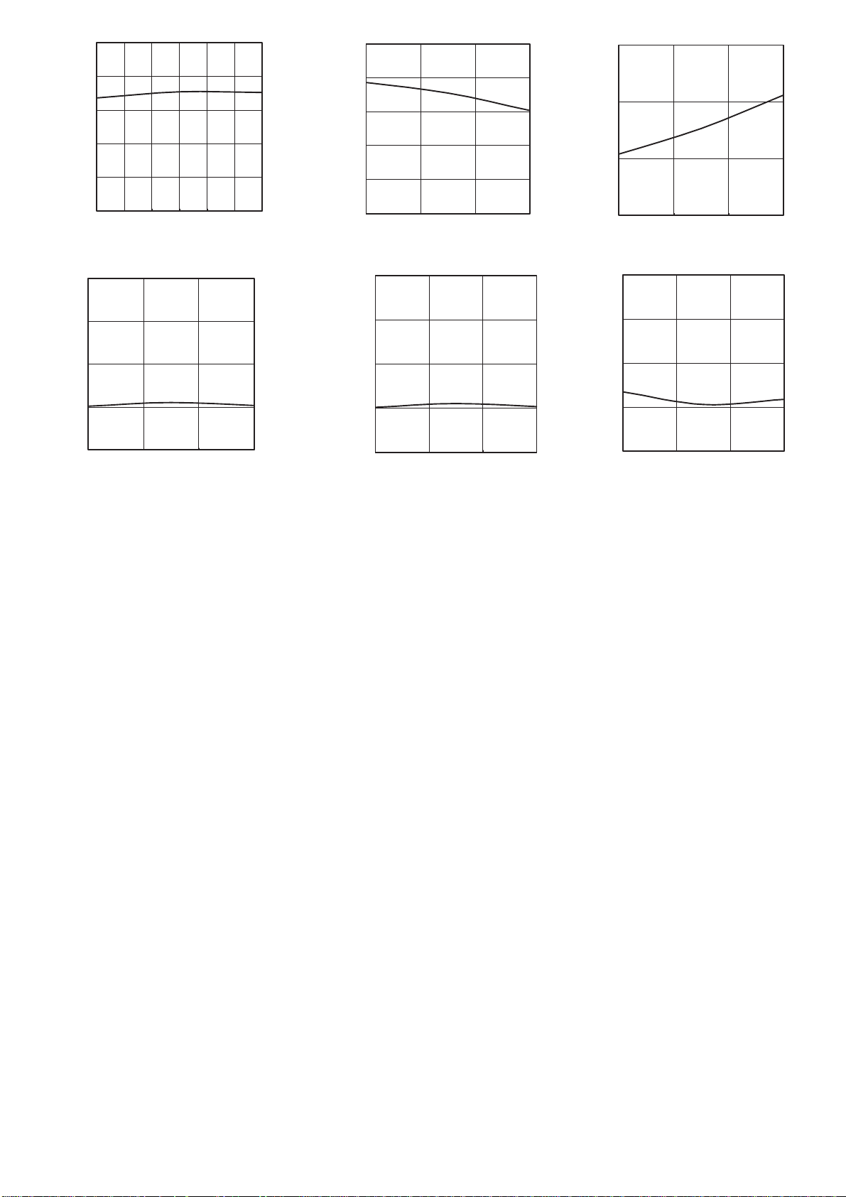
٨Reference data
4.5
4.4
[mA]
CC1
4.3
4.2
4.1
CIRCUIT CURRENT : I
4
3.9
-50 0 50 100
Fig3. Circuit Current1
TEMPERATURE [㷄]
10
0
GAIN
-10
-20
PHASE
GAIN [dB]
-30
-40
100C
100C
-50C
25C
-50C
25C
-50
1.00E+021.00E+031.00E+041.00E+051.00E+061.00E+071.00E+
Fig6. Frequency characteristic
Temperature dependence
FREQUENCY[Hz]
FS_L1_OUT
24
L1_L_IN
23
L1_L_OUT
22
L1_R_IN
21
L1_R_OUT
20
GND
19
FS_AUX_OUT
18
AUX_L_IN
17
AUX_L_OUT
16
AUX_R_IN
15
AUX_R_OUT
14
13
+5V
-5V
TU_R_IN
TU_L_IN
DA_R_IN
DA_L_IN
0.1u
ASW1
1
ASW2
2
+5V
3
47u0.1u
TU_R_IN
4
TU_L_IN
5
ASW3
6
ASW4
7
DA_R_IN
8
DA_L_IN
9
FS_L1_IN
10
-5V
11
47u
FS_AUX_IN +12V
12
FS_L1 OUT
FS_AUX OUT
12V
H
6.7V
M
L
12V
H
6.7V
M
L
Fig.2
ASW1, 2, 3, 4, FS_L1_IN, FS_AUX_IN are controlled by I
12
10
[mA]
CC2
8
6
4
CIRCUIT CURRENT:I
2
0
-50 0 50 100
TEMPERATURE [㷄]
Fig4. Circuit Current2
㪈㪌㪇
㪈㪇㪇
㪌㪇
㪇
㪄㪌㪇
㪄㪈㪇㪇
㪄㪈㪌㪇
08
㪲㩼㪴
㪛㪠㪪
PHASE [deg]
㪛㪠㪪㪫㪦㪩㪫㪠㪦㪥㩷㪑㩷㪝
0.1
0.01
0.001
4.4 4.6 4.8 5 5.2 5.4 5.6
㪪㪬㪧㪧㪣㪰㩷㪭㪦㪣㪫㪘㪞㪜㩷㪑㪭㪚㪚㪈㩷㪲㪭㪴
Fig7. Distortion
voltagedependence
6/8
FS_L1_OUT
10k
L1_L_IN
L1_L_OUT
47k
L1_R_IN
L1_R_OUT
47k
GND
FS_AUX_OUT
10k
AUX_L_IN
AUX_L_OUT
47k
AUX_R_IN
AUX_R_OUT
47k
+12V
47u0.1u
2
C-BUS of BH7624KS2.
10
GAIN
0
5.6V
-10
PHASE
-20
GAIN [dB]
-30
-40
-50
1.00E+021.00E+031.00E+041.00E+051.00E+061.00E+071.00E+
5.0V
4.4V
5.6V
5.0V
4.4V
FREQUENCY[Hz]
Fig5. Frequency characteristics
Supply voltage dependence
0.1
㪲㩼㪴
㪛㪠㪪
㪛㪠㪪㪫㪦㪩㪫㪠㪦㪥㩷㪑㩷㪝
㪣
0.01
㪩
0.001
-50 0 50 100
㪫㪜㪤㪧㪜㪩㪘㪫㪬㪩㪜㪲㷄㪴
Fig8. Distortion
(Temperature dependence)
㪈㪌㪇
㪈㪇㪇
㪌㪇
㪇
PHASE [deg]
㪄㪌㪇
㪄㪈㪇㪇
㪄㪈㪌㪇
08
Page 7
100
(
)
100
250
㪪㪆㪥㩷㪑㩷㪝㪪㪥㪲㩼㪴
98
96
94
92
98
96
94
㪪㪆㪥㩷㪑㩷㪝㪪㪥㪲㩼㪴
92
㪲㱅㪴
㪦㪥
㪩㪦㪥㩷㪑㩷㪩
200
150
90
4.4 4.6 4.8 5 5.2 5.4 5.6
-80
㪪㪬㪧㪧㪣㪰㩷㪭㪦㪣㪫㪘㪞㪜㩷㪑㪭㪚㪚㪈㩷㪲㪭㪴
Fig9. S/N ratio
(Supply voltage Dependence)
-85
-90
90
-50 0 50 100
㪫㪜㪤㪧㪜㪩㪘㪫㪬㪩㪜㪲㷄㪴
Fig10. S/N ratio
Temperature dependence
-80
㪲㪻㪙㪴
-85
㪪㪮㪚㪩㪪㪉
㪃㪝
㪪㪮㪚㪩㪪㪈
-90
100
-50 0 50 100
㪫㪜㪤㪧㪜㪩㪘㪫㪬㪩㪜㩷㪲㷄㪴
Fig11. ON Resistance
-80
㪲㪻㪙㪴
㪚㪟㪚㪩㪪㪉
-85
㪈㪃㪝
㪚㪟㪚㪩㪪
-90
-95
㪘㪪㪮㩷㪚㪩㪦㪪㪪㪫㪘㪣㪢㩷㪑㩷㪝㪪㪮㪚㪩㪪㪈㪃㪝㪪㪮㪚㪩㪪㪉㪲㪻㪙㪴
-100
-50 0 50 100
㪫㪜㪤㪧㪜㪩㪘㪫㪬㪩 㪜㩷㪲㷄㪴
Fig12. MUTE Attenuation
-95
㪘㪪㪮㩷㪚㪩㪦㪪㪪㪫㪘㪣㪢㩷㪑㩷㪝
-100
-50 0 50 100
㪫㪜㪤㪧㪜㪩㪘㪫㪬㪩㪜㩷 㪲㷄㪴
Fig13. ASW Crosstalk
٨Cautions on use
1. Numbers and data in entries are repr esentative design values and are not guaranteed values of the items.
2. Although ROHM is confident that the example application circuit reflects the best possible recommendations, be sure to
verify circuit characteristics for your particular application. Modification of constants for other externally connected
circuits may cause variations in both static and transient characteristics for external components as well as this Rohm IC.
Allow for sufficient margins when determining circuit constants.
3. Absolute maximum ratings
Use of the IC in excess of absolute maximum ratings, such as the applied voltage or operating temperature range
(Topr), may result in IC damage. Assumptions should not be made regarding the state of the IC (short mode or open
mode) when such damage is suffered. A physical safety measure, such as a fuse, should be implemented when using
the IC at times where the absolute maximum ratings may be exceeded.
4. -5V pin potential
Ensure a minimum -5V pin potential in all operating conditi ons. Make sure that no pins are at a voltage below the -5V
pin at any time, regardless of whether it is a transient signal or not. <GND=0V>
5. Thermal design
Perform thermal design, in which there are adequate margins, by taking into account the permissible dissipation (Pd)
in actual states of use.
6. Short circuit between terminals and erroneous mounting
Pay attention to the assembly direction of the ICs. Wrong mounting direction or shorts between terminals, GND, or other
components on the circuits, can damage the IC.
7. Operation in strong electromagnetic field
Using the ICs in a strong electromagnetic field can cause operation malfunction.
8. Supply voltage
Although basic circuit function is guaranteed under normal voltage operation (5V: ±4.5㨪5.5V, 12V: 11.5㨪12.5V),
ensure each parameter complies with appropriate electrical characteristics, when using th is device.
9. The application circuitry example
SW and FS output are controlled by BD3825FS which in turn is controlled by BH7624KS2 and therefore, BD38 25FS
and BH7624KS2 should be used in conjunction. Pins 18 and 24 should be pulled down by 10kȍ resistor. Pins 1, 2, 6,
7, 10, 12 must be controlled by the microcontroller when using BD3825FS on its own.
-95
㪚㪟㪘㪥㪥㪜㪣㩷㪚㪩㪦㪪㪪㪫㪘㪣㪢㪑㪝
-100
-50 0 50 100
㪫㪜㪤㪧㪜㪩㪘㪫㪬㪩㪜㩷 㪲㷄㪴
Fig14. Channel Crosstalk
7/8
Page 8

㧔
y
p
p
Ͷ Selection of order type
B D
SSOP-A24
<Dimension>
7.8 ± 0.3
1.8 ± 0.1
5.4 ± 0.2
0.11
10.0 ± 0.2
24
1
0.8
13
12
0.36± 0.1
3
0.3Min.
0.15 ± 0.1
0.1
8
TYPE
BD3825FS
Unit:mm)
2
5
F
<<Tape and Reel information>
Tape
Quantit
Direction
of feed
Embossed carrier ta
2000
cs
E2
(Correct direction: 1pin of product should be at the upper left when you hold
reel on the left hand, and you pull out the tape on the right hand)
1234
1234
Reel
Orders are available in complete units only.
1234
S
1pin
E
2
Package, Foaming specification
e
1234
1234
Direction of feed
1234
1234
1234
The contents described herein are correct as of October, 2005
The contents described herein are subject to change without notice. For updates of the latest information, please contact and confirm with ROHM CO.,LTD.
Any part of this application note must not be duplicated or copied without our permission.
Application circuit diagrams and circuit constants contained herein are shown as examples of standard use and operation. Please pay careful attention to the peripheral conditions when designing circuits and deciding
upon circuit constants in the set.
Any data, including, but not limited to application circuit diagrams and information, described herein are intended only as illustrations of such devices and not as the specifications for such devices. ROHM CO.,LTD. disclaims any
warranty that any use of such devices shall be free from infringement of any third party's intellectual property rights or other proprietary rights, and further, assumes no liability of whatsoever nature in the event of any such
infringement, or arising from or connected with or related to the use of such devices.
Upon the sale of any such devices, other than for buyer's right to use such devices itself, resell or otherwise dispose of the same, implied right or license to practice or commercially exploit any intellectual property rights or other
proprietary rights owned or controlled by ROHM CO., LTD. is granted to any such buyer.
The products described herein utilize silicon as the main material.
The products described herein are not designed to be X ray proof.
Published by
Application Engineering Group
Catalog NO.05T398Be '05.10 ROHM C 2000 TSU
Page 9
Appendix
Notes
No technical content pages of this document may be reproduced in any form or transmitted by any
means without prior permission of ROHM CO.,LTD.
The contents described herein are subject to change without notice. The specifications for the
product described in this document are for reference only. Upon actual use, therefore, please request
that specifications to be separately delivered.
Application circuit diagrams and circuit constants contained herein are shown as examples of standard
use and operation. Please pay careful attention to the peripheral conditions when designing circuits
and deciding upon circuit constants in the set.
Any data, including, but not limited to application circuit diagrams information, described herein
are intended only as illustrations of such devices and not as the specifications for such devices. ROHM
CO.,LTD. disclaims any warranty that any use of such devices shall be free from infringement of any
third party's intellectual property rights or other proprietary rights, and further, assumes no liability of
whatsoever nature in the event of any such infringement, or arising from or connected with or related
to the use of such devices.
Upon the sale of any such devices, other than for buyer's right to use such devices itself, resell or
otherwise dispose of the same, no express or implied right or license to practice or commercially
exploit any intellectual property rights or other proprietary rights owned or controlled by
ROHM CO., LTD. is granted to any such buyer.
Products listed in this document are no antiradiation design.
The products listed in this document are designed to be used with ordinary electronic equipment or devices
(such as audio visual equipment, office-automation equipment, communications devices, electrical
appliances and electronic toys).
Should you intend to use these products with equipment or devices which require an extremely high level
of reliability and the malfunction of which would directly endanger human life (such as medical
instruments, transportation equipment, aerospace machinery, nuclear-reactor controllers, fuel controllers
and other safety devices), please be sure to consult with our sales representative in advance.
It is our top priority to supply products with the utmost quality and reliability. However, there is always a chance
of failure due to unexpected factors. Therefore, please take into account the derating characteristics and allow
for sufficient safety features, such as extra margin, anti-flammability, and fail-safe measures when designing in
order to prevent possible accidents that may result in bodily harm or fire caused by component failure. ROHM
cannot be held responsible for any damages arising from the use of the products under conditions out of the
range of the specifications or due to non-compliance with the NOTES specified in this catalog.
Thank you for your accessing to ROHM product informations.
More detail product informations and catalogs are available, please contact your nearest sales office.
ROHM Customer Support System
www.rohm.com
THE AMERICAS / EUROPE / ASIA / JAPAN
Contact us : webmaster@ rohm.co. jp
Copyright © 2008 ROHM CO.,LTD.
21 Saiin Mizosaki-cho, Ukyo-ku, Kyoto 615-8585, Japan
TEL : +81-75-311-2121
FAX : +81-75-315-0172
Appendix1-Rev2.0
 Loading...