

Page 1
Video/Audio Interfaces for TV and DVD Recorders
NTSC-PAL Audio I/O
Interface for Recording/Playing
BD3822FS, BD3824FS
ƔDescription
BD3822FS and BD3824FS are the audio selectors with internal input selector, gain amp, ALC and power save ON/OFF functions.
BD3822FS contains the 1/2 power compression amp for level meter and 2ch volume. BD3824FS contains the line amp.
BD3822FS and BD3824FS unify the board pattern by pin compatible, and can be used individually as a high-end and low-end
model.
ƔFeatures
1) Low distortion (0.0015%) and low noise (3.2μVrms) by using a resistance ladder type circuit for volume. Shock sound in
switching is also reduced (BD3822FS)
2) Low distortion (0.0015%) and low noises (2.3μVrms)(BD3824FS)
3) Contains an ALC circuit, and can also be used as an RF output
4) Best suited to energy-saving design by low current consumption by using the Bi-CMOS process; compact regulator in the
set, being advantageous to heating in terms of quality
5) SSOP-A32 is used for package. The PCB layout can be easy and the area of PCB is reduced by putting sound input
terminals together, and output terminals, too.
6) BD3822FS and BD3824FS can be used with the same PCB board.
2
C BUS data format of BD3822FS is upward compatible with BD3824FS, and can be used without changing the software.
7) I
8) A system is employed, in which the waveform connected to the input (tuner, Front, Ext) is not distorted even in standby
m o d e .
ƔApplications
DVD recorder
ƔProduct lineup
TECHNICAL NOTE
Function BD3822FS BD3824FS
Volume function Available -
1/2 power compression amp Available -
Line amp - Available
Circuit current (mA) 7 6.4
Output noise (μVrms) 3.2 2.3
BD3822FS is an upstream compatible IC with BD3824FS.
Ver.B Oct.2005
Page 2
ƔAbsolute maximum ratings (Ta=25qC)
Parameter Symbol Limits Unit
Applied voltage VCC 10.0 V
Input voltage VIN VCC+0.3GND-0.3 V
Power Dissipation Pd 950
*1
mW
Operating temperature Topr -40+85 *2 qC
Storage temperature Tastg -55+150 qC
*1 Reduced by 7.6 mW/qC at 25qC or higher.
Thermal resistance Tja = 131.6 (°C/W), when Rohm standard board is mounted.
3
Rohm standard board : Size: 70701.6 (mm
)
Material: FR4 glass-epoxy substrate (copper foil area: not more than 3%).
*2 As long as voltage stays within operating voltage range, certain circuit operation is guaranteed in the operating
temperature range.
Allowable power loss conditions are related to temperature, to which care must be taken.
In addition though the standard value of its electrical characteristics cannot be guaranteed under the conditions
other than those specified, basic functions are maintained.
ƔOperating range (Basic operation at Ta25qC)
Parameter Symbol Min. Typ. Max. Unit
Power Supply voltage *3 VCC 7.0 - 9.5 V
*3 As long as temperature and operating voltage meet specifications
In addition, though the standard value of its electrical characteristics cannot be guaranteed under the conditions
other than those specified, basic functions are maintained.
2/8
Page 3
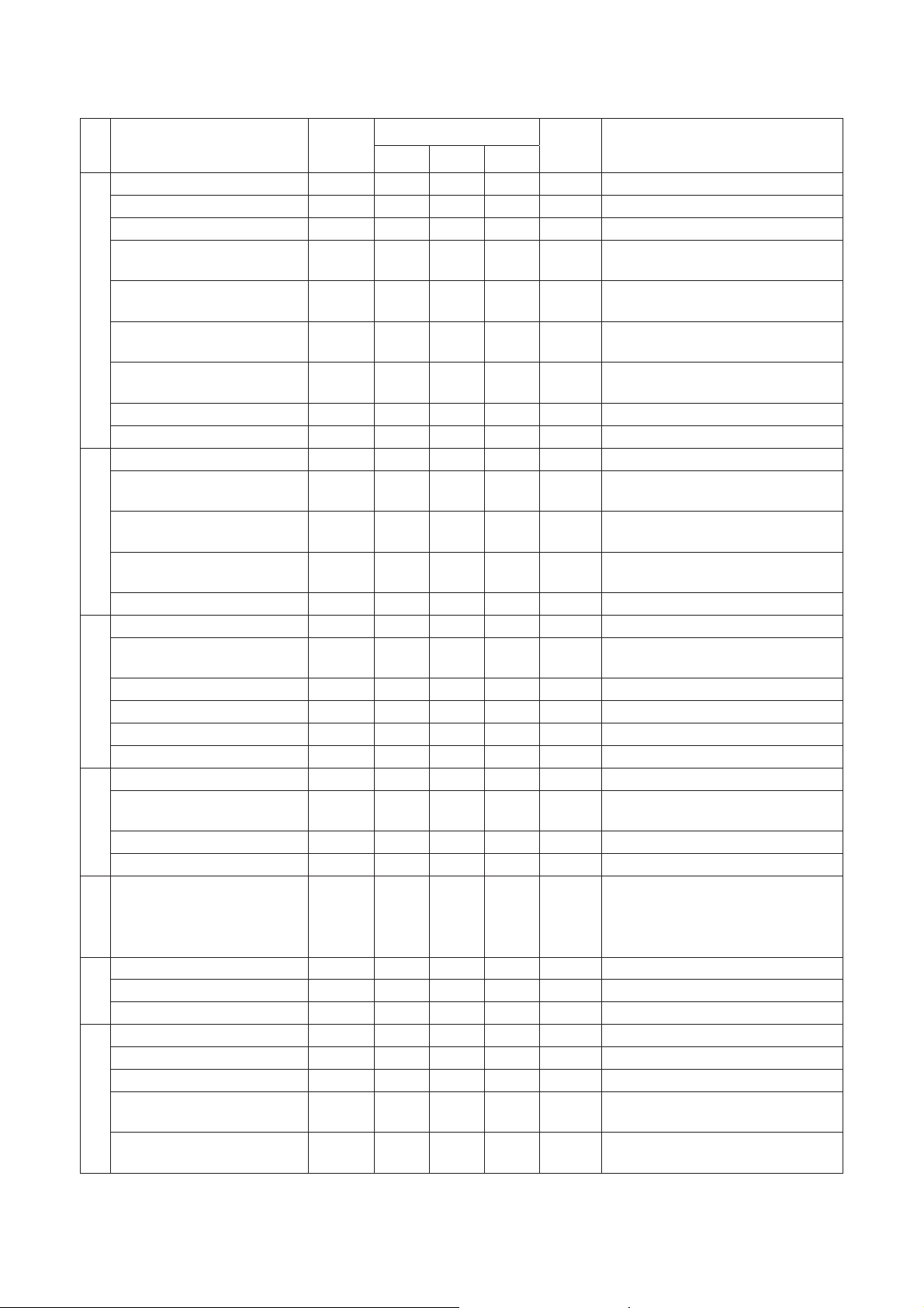
Ɣ Electric characteristics BD3822FS
(Unless specified: Ta=25, VCC=9V, f=1kHz, V
=1Vrms, Rg=600Ԉ, RL=10kԈ,Gain Amp=0dB,Volume=0dB,
IN
Input terminal=Front1,Output Terminal=OUT1)
Parameter Symbol
Min. Typ. Max.
Circuit current upon no signal IQ - 7 30 mA VIN=0Vrms
Standby current IOFF - 540 1000 μA £Power OFF¤ MODE
Voltage gain GV -1.5 0 1.5 dB GV=20log(VOUT/VIN)
Maximum output voltage VOM 2.0 2.5 - Vrms
Channel balance CB -1.5 0 1.5 dB
GENERAL
Total harmonic distortion THD - 0.0015 0.05 %
Output noise voltage * VNO - 3.2 16 μVrms
Residual noise voltage * VNOR - 2 10 μVrms Volume = -dB,Rg = 0Ԉ, BW=IHF-A
Cross-talk between channels * CTC - -110 -80 dB Rg = 0ԈBW = IHF-A
Input impedance RIN 77 110 143 kԈ *1)
Maximum input voltage VIM 2.1 2.5 - Vrms
Cross-talk between selector CTS - -110 -80 dB
INPUT
Tuner gain GTU 10 12 14 dB
Output offset voltage VDC -20 0 20 mV Tuner SAPΦFront1
Volume control range VV1 -81 -78 -75 dB GV=20log(VOUT/VIN),BW = IHF-A
Maximum attenuation GV MIN1 - -106 -85 dB
Step resolution 1 GV STEP1 - 1 - dB Volume=0-46dB
Step resolution 2 GV STEP2 - 2 - dB Volume=-46-78dB
VOLUME
Attenuation set error 1 GV ERR1 -2 0 2 dB Volume=0-58dB
Attenuation set error 2 GV ERR2 -3 0 3 dB Volume=-60-78dB
Minimum gain GMIN -1.5 0 1.5 dB Gain Amp=0dB,G=20log(VOUT/VIN)
Maximum gain G MAX 4.5 6 7.5 dB
Step resolution G STEP - 0.2 - dB 4.6dB to 5.6dB
GAIN AMP
Gain set error G ERR -1.5 0 1.5 dB
Mute attenuation GMUTE - -110 -85 dB
MUTE
ALC I/O level 1 ALC1 - -3 0 dBV Suppression level is set to -3dBV.
ALC I/O level 2 ALC2 - -5 -2 dBV Suppression level is set to -5dBV.
ALC
ALC I/O level 3 ALC3 - -7 -4 dBV Suppression level is set to -7dBV.
Output offset voltage VDC OFF - 30 100 mV VIN =0dBV
DC maximum output voltage VDC MAX 2.9 3.7 - V VIN =+6dBV
DC standard output voltage VDC ST 1.1 1.5 1.9 V VIN =-10dBV
DC voltage difference between
channels
Square-Law
Compression Amp
DC output voltage linearity
ͼVDC -250 0 250 mV VIN =-10dBV
ͼVDC/
ͼV
0.9 1.4 1.9 V V
IN
*1: 1) Refers to 1,2,3,9,10,11,12,13,14,25,26,31,32 pin terminals.
Limits
Unit Conditions
VOM at THD(VOUT)=1%
BW=400-30KHz
CB = GV1-GV2
GV1:ch1Gain GV2:ch2 Gain
VIN=2Vrms,Volume=-12dB
Gain Amp=5.6dB,BW=400-30KHz
Volume=-12dB,Gain Amp=5.6dB
Rg = 0Ԉ, BW=IHF-A
VIM at THD(VOUT)=1%
BW=400-30KHz *1)
Rg = 0ԈBW = IHF-A
CTS=20log(VOUT/VIN)
Tuner gain=12dB, VIN=0.25Vrms
G=20log(VOUT/VIN)
Volume = -dB, BW = IHF-A
V=20log(VOUT/VIN)
G
Gain Amp=6dB,VIN=500mVrms
G=20log(VOUT/VIN)
Mute ON
GMUTE=20log(VOUT/VIN)
BW = IHF-A
Volume=-dB, or -78dB
IN =-30-6dBV
3/8
Page 4

Ɣ Electric characteristics BD3824FS
(Unless specified: Ta=25, VCC=9V, f=1kHz, V
Input terminal=Front1,Output Terminal=OUT1)
Circuit current upon no signal
Standby current
Voltage gain
Maximum output voltage 1
Maximum output voltage 2
Parameter Symbol
Q - 6.4 19.2 mA VIN=0Vrms
I
OFF - 940 1760 μA
I
V -7.6 -6.1 -4.6 dB
G
OM1 1.68 2.1 - Vrms
V
VOM2 2.0 2.5 - Vrms
GENERAL
OM3 2.2 2.5 - Vrms
Maximum output voltage 3
Channel balance
Total harmonic distortion
Output noise voltage *
Cross-talk between channels *
Input impedance
Maximum input voltage
Cross-talk between selector *
V
CB -1.5 0 1.5 dB
THD -
NO - 2.3 11.5 μVrms
V
CTC - -100 -80 dB
IN 77 110 143
R
IM 2.1 2.5 - Vrms
V
CTS - -105 -80 dB
INPUT
TU 10 12 14 dB
Tuner gain
Output offset voltage
Minimum gain
Maximum gain
GAINAMP
G
DC -20 0 20 mV
V
MIN -1.5 0 1.5 dB
G
MAX 3.5 5 6.5 dB
G
=1Vrms, Rg=600Ԉ, RL=10kԈ,Gain Amp=0dB,Volume=0dB,
IN
Limits
Unit Conditions
Min. Typ. Max.
Power OFF MODE
V=20log(VOUT/VIN), RL2=10kԈ
G
Output terminal =
OUT1/OUT2, RL2=10kԈ
OM at THD(VOUT)=1%
V
Gain Amp=5dB,
BW=400-30kHz
Output terminal=RF OUT
VOM at THD(VOUT)=1%
ALC=OFF, RL2=10kԈ
BW=400-30kHz
Output terminal=
LINE OUT1/LINE OUT2
OM at THD(VOUT)=1%
V
RL1=4.7kԈ
External LPF Gvc=6dB
BW=400-30kHz
V1-GV2
CB = G
GV1:ch1Gain GV2:ch2 Gain
0.0015
0.05 % VIN=2Vrms,BW=400-30KHz
Rg = 0Ԉ, BW=IHF-A
Rg = 0Ԉ,BW = IHF-A
kԈ
*2)
VIM at THD(VOUT)=1%
BW=400-30KHz*2)
Rg = 0Ԉ,BW = IHF-A
CTS=20log(VOUT/VIN)
Tuner gain=12dB
V
IN=0.25Vrms,
G=20log(VOUT/VIN)
Tuner1ΦFront1,
Tuner Gain = 8dB
Gain Amp=0dB
G=20log(VOUT/VIN)
Gain Amp=5dB,VIN=500mVrms
G=20log(VOUT/VIN)
Mute attenuation
MUTE - -110 -85 dB
G
Mute ON, BW = IHF-A
GMUTE=20log(VOUT/VIN)
RF MUTE
ALC I/O level 1
ALC I/O level 2
ALC
ALC I/O level 3
ALC1
ALC2
ALC3
- -3 0 dBV
- -5 -2 dBV
- -7 -4 dBV
Suppression level is set to -3dBV.
Suppression level is set to -5dBV.
Suppression level is set to -7dBV.
1. *2) Refers to 2,3,9,10,11,12,13,14,31,32pin terminals.
2. VP-9690A (Average value detection, effective value display) IHF-A filter by Matsushita Communication is used fo measurement.
3. Phase between input/output is the same.
4. This IC is not designed to be radiation-resistant.
4/8
Page 5

ƔExample of application circuit
A
k
(
)
(
r
r
ȝ
ȝ
R
A
ȝ
R
A
R
k
Front1
1 ȝ
+
C
24 C 23
(Ch1) (Ch2)
Front2
+
/D
10
ȝ
1 ȝ
30 29 31 32 24
10 ȝ
+
21
C
C
22
DVD
D/A
2.2M
4.7ȝ
ȝ
+
C
20
27
+
C19C
26
28 18
VCC
0,4.6,4.8,5.0,5.2,5.4,5.6,6.0dB
VOL
dB
0 -78dB,
-
0- 78dB,-
INPUT SELECTO
LINE
OUT
OUT
C
10
1
1ȝ
+
+
C
17
dB
C
18
25
15
10
16
CC
V
LC
1/2VCC
GND
SDA
21
2
I
C BUS
LOGIC
SCL
20
Powe
ON/OFF
4
ON/OFF
8,12dB
1
ȝ
1
+
C
2
1 ȝ 1 ȝ
(Ch1) (Ch2)
+
C
3
+
C
4
0.33 ȝ
C
C
6
5
10 ȝ
10 ȝ
+
C
1
(Ch1)
+
Ch2
+
C
C
8
7
10ȝ
0.33ȝ
9876 5 4 3 2
Ch1)(Ch2) (Ch1) (Ch2) (Ch1)
+
+
9
1 ȝ
C
C
11
10
1ȝ
+
1 ȝ
+
C
12
Ԝ
1
+
C
C
13
ȝ
1
Tuner1
Tuner2 CAP1
SAP_O Tuner1_0 Tuner2_0
Tuner
SAP
EXT1 1 EXT1 2 EXT2 1 EXT2 2 EXT3 1
CAP2
EXT3 2
Fig.1 Example of application circuit (BD3822FS)
19
Powe
14
47
(Ch2)
+
1 ȝ
330
DC2
C
R
4.7 ȝ 330k 4.7 ȝ
DET1
Unit
DC1
MP2
DET2
R : [Ԉ]
C : [F]
C
5/8
Page 6

ƔExample of application circuit
-
ge (
)
-
-
A
r
(
) (
)
T
ȝ
ȝ
ȝ
Front1
Front2
ȝ
1
C
28 C 27
Ch1
ȝ
Ch2
VCC
30 29 31 32
C26
10
0,5dB
/D
OUT1 OUT2
ȝ
10
ȝ
C
25
0,5dB
10
C
DVD
LINE
OUT1
10
ȝ
24
D/A
LINE
C
C
20
1ȝ
R5
C
23
+
R
7
R
6
C21
C22
27
28
C
26
OUT2
17
1ȝ
C
16
R
2
10ȝ
+
R
4
R
3
18
C19
24 23
25
VCC
VCC
-6.1dB
-6.1dB
INPUT SELECTOR
0,8,12dB
0,8,12dB
1
N.C.
(Ch2)
(Ch1)
C
C
1
ȝ
1
N.C.
2
ȝ
1
Tuner2
Tuner1
5
6
432
N.C.
(Ch1)
C
3
10
Tuner1_0
C
4
10ȝ
Tuner2_0
(Ch2)
C
5
CAP1
(Ch1) (Ch2) (Ch1) (Ch2) (Ch1) (Ch2)
C
C
6
ȝ
1
EXT11
Fig.2 Example of application circuit (BD3824FS)
ƔReference dat a
10
10
8
6
4
2
QUIESCENT CURRENT : IQ [mA]
0
0
2 4 6 810
SUPPLY VOLTAGE : VCC[V]
Fig.3 Quiescent current vs
Supply voltage (BD3822FS)
85C
25C
40C
8
6
4
2
QUIESCENT CURRENT : IQ[mA]
0
0246
SUPPLY VOLTAGE : VCC[V]
Fig.4 Quiescent current vs
Supply voltage (BD3824FS)
6/8
85C
FILTER GND
C
15
ȝ
10
22
1/2VCC
C
7
8
Ԝ
EXT12 EXT21
25C
40C
810
Powe
OFF
19
SCL SDA
20 21
GND
I2C BUS
LOGIC
Power
OFF
ALC
R
1
C
C
Ԝ
C
EXT22
0.0001
TOTAL HARMONIC DISTORTION : THD+N[%]
9
ȝ
5
1
0.1
0.01
0.001
1m
11
10
EXT31
OUTPUT VOLTAGE : V
ȝ
EXT32
ȝ
100m
Fig.5 Total harmonic distortion vs
Output volta
OU
ȝ
10
C
18
15 1614 13 121110987
C
4.7ȝ 2.2M
Unit
25C
40C
OUT[Vrms]
BD3822FS
SELECT
14
17
12
4.7ȝ
RF BIAS
R : [Ԉ]
C : [F]
85C
1
VCC
C13
3 10m
Page 7

-
-
-
-
(
)
5
1
0.001
0.0001
TOTAL HARMONIC DISTORTION : THD+n
0.1
0.01
1m
OUTPUT VOLTAGE : VOUT [Vrms]
25C
40C
100m
Fig.6 Total harmonic distortion vs
Output voltage (BD3824FS)
+10
+8
+6
85C
3 10m
1
+4
+2
0
-2
-4
VOLTAGE GAIN : GV [dB]
-6
-8
-10
10 100k 10k 100 1k
FREQUENCY : f [Hz]
Fig.7 Voltage gain vs Frequency
(BD3822FS)
0
-4
-8
-12
VOLTAGE GAIN : GV [dB]
-16
-20
10 100k 10k 100 1k
FREQUENCY : f [Hz]
Fig.8 Voltage gain vs Frequency
(BD3824FS)
-
5
1
100m
10m
1m
OUTPUT VOLTAGE : VOUT [Vrms]
100u
1m
10m 100m
INPUT VOLTAGE : VIN [Vrms]
Fig.9 ALC I/O characteristic 㩷㩷㩷
(BD3822FS)
3dBV
5dBV
7dBV
1
5
ƔOperation Notes
1. Numbers and data in entries are representative design values and are not guaranteed values of the items.
2. Although ROHM is confident that the example application circuit reflects the best possible recommendations, be sure to verify
circuit characteristics for your particular application. Modification of constants for other externally connected circuits may cause
variations in both static and transient characteristics for external components as well as this Rohm IC. Allow for sufficient
margins when determining circuit constants.
3. Absolute maximum ratings
Use of the IC in excess of absolute maximum ratings, such as the applied voltage or operating temperature range (Topr), may
result in IC damage. Assumptions should not be made regarding the state of the IC (short mode or open mode) when such
damage is suffered. A physical safety measure, such as a fuse, should be implemented when using the IC at times where the
absolute maximum ratings may be exceeded.
4. GND potential
Ensure a minimum GND pin potential in all operating conditions. Make sure that no pins are at a voltage below the GND at any
time, regardless of whether it is a transient signal or not.
5. Thermal design
Perform thermal design, in which there are adequate margins, by taking into account the permissible dissipation (Pd) in actual
states of use.
6. Short circuit between terminals and erroneous mounting
Pay attention to the assembly direction of the ICs. Wrong mounting direction or shorts between terminals, GND, or other components
on the circuits, can damage the IC.
7. Operation in strong electromagnetic field
Using the ICs in a strong electromagnetic field can cause operation malfunction.
5
4
3
2
1
OUTPUT VOLTAGE : VOUT [V]
0
0
500m
INPUT VOLTAGE : VIN [Vrms]
1.5 1 2.5 2
Fig.10 Square-Low Compression amp
I/O characteristic (BD3824FS)
3
[Vrms]
OUT
2
1
0
MAXIMUM OUTPUT VOLTAGE : V
100
LOAD RESISTANCE : RL [Hz]
10000
Fig.11 Output load characteristic
BD3822FS, BD3824FS
100000 1000
7/8
Page 8

ƔSelection of order type
SSOP-A32
<Dimension>
7.8 ± 0.3
1.8 ± 0.1
5.4 ± 0.2
0.11
32
1
0.8
13.6 ± 0.2
0.36 ± 0.1
17
16
Part No.
BD3822FS
BD3824FS
0.3Min.
0.15 ± 0.1
0.1
Unit:mm)
<Tape and Reel information>
Tape
Quantity
Direction
of feed
Embossed carrier tape
2000pcs
E2
(Correct direction: 1pin of product should be at the upper left when you hold reel
on the left hand, and you pull out the tape on the right hand)
1234
Reel
1234
1234
ESF 2 2 8 3 D B
2
Tape and Reel information
1234
1234
1234
1234
1pin
Direction of feed
Orders are available in complete units only.
1234
The contents described herein are correct as of October, 2005
The contents described herein are subject to change without notice. For updates of the latest information, please contact and confirm with ROHM CO.,LTD.
Any part of this application note must not be duplicated or copied without our permission.
Application circuit diagrams and circuit constants contained herein are shown as examples of standard use and operation. Please pay careful attention to the peripheral conditions when designing circuits and deciding
upon circuit constants in the set.
Any data, including, but not limited to application circuit diagrams and information, described herein are intended only as illustrations of such devices and not as the specifications for such devices. ROHM CO.,LTD. disclaims any
warranty that any use of such devices shall be free from infringement of any third party's intellectual property rights or other proprietary rights, and further, assumes no liability of whatsoever nature in the event of any such
infringement, or arising from or connected with or related to the use of such devices.
Upon the sale of any such devices, other than for buyer's right to use such devices itself, resell or otherwise dispose of the same, implied right or license to practice or commercially exploit any intellectual property rights or other
proprietary rights owned or controlled by ROHM CO., LTD. is granted to any such buyer.
The products described herein utilize silicon as the main material.
The products described herein are not designed to be X ray proof.
Published by
Application Engineering Group
8/8
Catalog NO.05T396Be '05.10 ROHM C 1000 TSU
Page 9

Appendix
Notes
No technical content pages of this document may be reproduced in any form or transmitted by any
means without prior permission of ROHM CO.,LTD.
The contents described herein are subject to change without notice. The specifications for the
product described in this document are for reference only. Upon actual use, therefore, please request
that specifications to be separately delivered.
Application circuit diagrams and circuit constants contained herein are shown as examples of standard
use and operation. Please pay careful attention to the peripheral conditions when designing circuits
and deciding upon circuit constants in the set.
Any data, including, but not limited to application circuit diagrams information, described herein
are intended only as illustrations of such devices and not as the specifications for such devices. ROHM
CO.,LTD. disclaims any warranty that any use of such devices shall be free from infringement of any
third party's intellectual property rights or other proprietary rights, and further, assumes no liability of
whatsoever nature in the event of any such infringement, or arising from or connected with or related
to the use of such devices.
Upon the sale of any such devices, other than for buyer's right to use such devices itself, resell or
otherwise dispose of the same, no express or implied right or license to practice or commercially
exploit any intellectual property rights or other proprietary rights owned or controlled by
ROHM CO., LTD. is granted to any such buyer.
Products listed in this document are no antiradiation design.
The products listed in this document are designed to be used with ordinary electronic equipment or devices
(such as audio visual equipment, office-automation equipment, communications devices, electrical
appliances and electronic toys).
Should you intend to use these products with equipment or devices which require an extremely high level
of reliability and the malfunction of which would directly endanger human life (such as medical
instruments, transportation equipment, aerospace machinery, nuclear-reactor controllers, fuel controllers
and other safety devices), please be sure to consult with our sales representative in advance.
It is our top priority to supply products with the utmost quality and reliability. However, there is always a chance
of failure due to unexpected factors. Therefore, please take into account the derating characteristics and allow
for sufficient safety features, such as extra margin, anti-flammability, and fail-safe measures when designing in
order to prevent possible accidents that may result in bodily harm or fire caused by component failure. ROHM
cannot be held responsible for any damages arising from the use of the products under conditions out of the
range of the specifications or due to non-compliance with the NOTES specified in this catalog.
Thank you for your accessing to ROHM product informations.
More detail product informations and catalogs are available, please contact your nearest sales office.
ROHM Customer Support System
www.rohm.com
THE AMERICAS / EUROPE / ASIA / JAPAN
Contact us : webmaster@ rohm.co. jp
Copyright © 2008 ROHM CO.,LTD.
21 Saiin Mizosaki-cho, Ukyo-ku, Kyoto 615-8585, Japan
TEL : +81-75-311-2121
FAX : +81-75-315-0172
Appendix1-Rev2.0
 Loading...