


Sound Processors for Home Theater Systems
6.1ch
Sound Processor
BD3816K1,BD3817KS
●Description
The BD3816K1 and BD3817KS are 6.1ch sound processors. Functions required for applications, such as AV receivers and
home theater systems, are integrated into a single chip. A wide dynamic range of 132dB is achieved by utilizing the
BiCMOS process.
●Features
1) Dynamic range: 132dB (Volume Direct Mode, VOL=MUTE, IHF-A)
2) Independent 7 channels for Master Volume (0 to -95 dB, MUTE 1dB/Step)
3) Supporting 2
4) Low current consumption design achieved by adopting the Bi-CMOS process.
5) Maximum output voltage: 4.2Vrms (VCC=7V, VEE=-7V, RL=10k).
6) Built-in Input Gain Amp useful for amplifying input signals (0-7dB, 1dB/Step).
7) Built-in Output Gain Amp useful for adjusting output signal voltages (0-17dB, 1dB/Step)
8) Built-in mixing circuit for distributing the output signals from Center and Subwoofer channel to Front R/L channels
(0, -3, -4.5dB).
9) 2ch Volume control BD3812F or 6ch Function Switch BD3843FS can be controlled simultaneously
by the serial control bus.
10) REC A output terminal with a REC input/output switch useful for monitoring Equalizer Amp.
(For BD3816K1, available as an input function of the seventh line.)
11) Output mute controlled by either serial data or an external control terminal.
12) 2-wire serial control (For both 3.3V and 5V)
●Applications
AV receivers, home theater systems, and mini-audio systems.
●Line up matrix
nd
room entertainment/2nd source recording.
No.10081EAT06
Parameter BD3816K1 BD3817KS
6(+1) inputs
Number of Input Selectors
Input Gain 0 ~ 7dB 1dB/step 0 ~ 7dB 1dB/step
Volume 0 ~ -95dB 1dB/step、7ch 0 ~ -95dB 1dB/step、7ch
Bass, Treble ±14dB 2dB/step ±14dB 2dB/step
Output Gain 0 ~ 17dB 1dB/step 0 ~ 17dB 1dB/step
Mix i n g Yes Yes
Package QFP80 SQFP100
www.rohm.com
© 2010 ROHM Co., Ltd. All rights reserved.
ROUTA terminal: available as
an input selector of the seventh line
1/17
10 inputs, 2 outputs
2010.06 - Rev.A

BD3816K1,BD3817KS
●Absolute maximum ratings (Ta=25℃)
Parameter Symbol Ratings Unit
Technical Note
Power Supply Voltage
Power Dissipation Pd
VCC 7.5 *1
VEE -7.5
1200 (BD3816K1)
1300 (BD3817KS)
*2 mW
Operating Temperature Range Topr -20 ~ +75 ℃
Storage Temperature Range Tstg -55 ~ +125 ℃
*1 Even in the specified range of Power Supply Voltage, applying voltage only to the VCC side may cause
an excessive current to give a permanent damage to the IC.
When starting up power supplies, VEE and VCC should be powered on simultaneously or VEE first; then followed by VCC.
*2 Reduced by 12 mW/℃ over 25℃ (BD3816K1), when installed on the standard board (size: 70x70x1.6mm).
Reduced by 13 mW/℃ over 25℃ (BD3817KS), when installed on the standard board (size: 70x70x1.6mm)
●Operating conditions
Must function normally at Ta=25C.
Parameter Symbol
Operating source voltage
Min. Typ. Max.
VCC 5.0 7.0 7.3
VEE -7.3 -7.0 -5.0
Ratings
Unit
●Electrical characteristics
Ta =2 5℃, V
CC=7V, f=1kHz, Vin=1Vrms, RL=10k, Rg=600, Input Gain=0dB, Volume=0dB, Output Gain=0dB, Bass=0dB,
Treble=0dB, Mixing c/sw=OFF, unless otherwise noted.
Parameter Symbol
Min. Typ. Max.
Limits
Unit Conditions
V
V
Circuit Current
VCC
IQ
- 24 40 mA No signal
VEE -40 -24 -
Output Voltage Gain Gv -2 0 2 dB
Total Harmonic Distortion Ratio THD - 0.001 0.03 % BW=400Hz-30kHz
Maximum Output Voltage Vomax 3.6 4.2 - Vrms THD=1%
Rg=0Ω, BW=IHF-A
(Output gain ON, Tone ON)
Rg=0Ω, BW=IHF-A
(Output gain ON, Tone OFF)
Rg=0Ω, BW=IHF-A
(*OM=Volume Direct)
Output Noise Voltage Vno
- 2.0 12 µVrms
- 1.5 8 µVrms
- 1.2 8 µVrms
Cross-talk between Channels CTC - -95 -80 dB Rg=0Ω, BW=IHF-A
Cross-talk between Selectors CTS - -95 -80 dB Rg=0Ω, BW=IHF-A
Volume Output Voltage GVV -2 0 2 dB
Volume Total Harmonic
Distortion Ratio
THDV - 0.001 0.03 % BW=400Hz-30kHz
Volume Output Noise Voltage VnoV - 1.2 8 µVrms Rg=0Ω, BW=IHF-A
www.rohm.com
© 2010 ROHM Co., Ltd. All rights reserved.
2/17
2010.06 - Rev.A

BD3816K1,BD3817KS
Parameter Symbol
Volume Control Range VOL -97.5 -95 -92.5 dB
Volume Setting Error 1 VOLE1 -1.5 0 1.5 dB
Volume Setting Error 2 VOLE2 -2.5 0 2.5 dB
Maximum Attenuation VOLmin - -115 -105 dB
Treble Maximum Boost Gain GTB 12 14 16 dB f=15kHz, Vin=0.4Vrms
Treble Maximum Cut Gain GTC -16 -14 -12 dB f=15kHz, Vin=0.4Vrms
Treble Step Resolution TR - 2 - dB f=15kHz, Vin=0.4Vrms
Treble Gain Setting Error TE -2 0 2 dB f=15kHz, Vin=0.4Vrms
Bass Maximum Boost Gain GBB 12 14 16 dB f=100Hz, Vin=0.4Vrms
Bass Maximum Cut Gain GBC -16 -14 -12 dB f=100Hz, Vin=0.4Vrms
Min. Typ. Max.
Limits
Unit Conditions
Vin=3Vrms
*OM=Volume Direct
0 to -53dB, Vin=3Vrms
*OM=Volume Direct
-54dB to -95dB, Vin=3Vrms
*OM=Volume Direct
Vin=3Vrms, BW=IHF-A
*OM=Volume Direct
Technical Note
Bass Step Resolution BR - 2 - dB f=100Hz, Vin=0.4Vrms
Bass Gain Setting Error BE -2 0 2 dB f=100Hz, Vin=0.4Vrms
C Mixing Gain Control Range GMCG -6.5 -4.5 -2.5 dB *OM=Volume Direct
C Mixing Gain Setting Error GMCE -2 0 2 dB *OM=Volume Direct
SW Mixing Gain Control Range
SW Mixing Gain Setting Error GMSWE -2 0 2 dB *OM=Volume Direct
Input Gain Control Range GIG 5 7 9 dB
Input Gain Setting Error GIE -2 0 2 dB
Output Gain Control Range GOG 15 17 19 dB
Output Gain Setting Error GOE -2 0 2 dB
ROUT Output Impedance RoutR - 20 100 Ω
ROUT Voltage Gain GVR -2 0 2 dB RL=47kΩ
ROUT Total Harmonic
Distortion Ratio
* OM:Output mode
GMSW
G
THDR - 0.005 0.09 % RL=47kΩ, BW=400Hz-30kHz
-6.5 -4.5 -2.5 dB *OM=Volume Direct
Vin=0.4Vrms
*OM=Volume Direct
Vin=0.4Vrms
*OM=Volume Direct
Vin=0.4Vrms
*OM=Output gain ON(Tone OFF)
Vin=0.4Vrms
*OM=Output gain ON(Tone OFF)
* Note: This IC is not designed to be radiation-resistant.
www.rohm.com
© 2010 ROHM Co., Ltd. All rights reserved.
3/17
2010.06 - Rev.A

BD3816K1,BD3817KS
●Timing chart
1) Signal Timing Cond itions
・Data is read on the rising edge of the clock.
・Latch is read out on the falling edge of the clock.
・Latch signal must terminate with the LOW state.
* To avoid malfunctions, clock and data signals must terminate with the LOW state.
1byte=17bit
CL
CLOCK
(
DA
DATA
LATCH
)
90% 90% 90%
Parameter Symbol
90% 90% 90% 90%
tsu
twd
DATA
twc
10% 10% 10%
twc
thd thd th ts tsl thl tsd
twh
10%
Fig. 1
Min. Typ. Max.
DATA
Limits
90% 90%
twl
10% 10%
LATCH
Unit
Technical Note
Terminate
with Low
Minimum Clock Width twc 1.0 - - µs
Minimum Data Width twd 1.0 - - µs
Minimum Latch Width twl 1.0 - - µs
LOW Hold Width twh 1.0 - - µs
Data Set-up Time (DATACLK) tsd 0.5 - - µs
Data Hold Time (CLKDATA) thd 0.5 - - µs
Latch Set-up Time (CLKLATCH) tsl 0.5 - - µs
Latch Hold Time (DATALATCH) thl 0.5 - - µs
Latch Low Set-up Time ts 0.5 - - µs
Latch Low Hold Time th 0.5 - - µs
2) Voltage Conditions for Control Signals
Parameter Condition
“H” Input Voltage
“L” Input Voltage 0 - 1.0 V
Vcc=5 ~ 7.3V
V
EE=-5 ~ -7.3V
Limits
Min. Typ. Max. (≦Vcc)
2.2 - 5.5 V
Unit
www.rohm.com
© 2010 ROHM Co., Ltd. All rights reserved.
4/17
2010.06 - Rev.A

BD3816K1,BD3817KS
3) Control Data Format List
Data input Direction
MSB LSB
D16 D15 D14 D13 D12 D11 D10 D9 D8 D7 D6 D5 D4 D3 D2 D1 D0
Data
(1)BD3816K1 Control Data Formats
D16 D15 D14 D13 D12 D11 D10 D9 D8 D7 D6 D5 D4 D3 D2 D1 D0
Data
①
FRL select
D16 D15 D14 D13 D12 D11 D10 D9 D8 D7 D6 D5 D4 D3 D2 D1 D0
Data
②
Data
③
Data
④
Data
⑤
Data
⑥
Data
⑦
Data
⑧
・By changing Select Address, eight different control formats are selectable.
・At power-on sequence, initialize all data.
(Example)
REC A
mode select
D16 D15 D14 D13 D12 D11 D10 D9 D8 D7 D6 D5 D4 D3 D2 D1 D0
D16 D15 D14 D13 D12 D11 D10 D9 D8 D7 D6 D5 D4 D3 D2 D1 D0
Input gain
FRLch
D16 D15 D14 D13 D12 D11 D10 D9 D8 D7 D6 D5 D4 D3 D2 D1 D0
Master volume
and Output gain
D16 D15 D14 D13 D12 D11 D0 D9 D8 D7 D6 D5 D4 D3 D2 D1 D0
Master volume
and Output gain
D16 D15 D14 D13 D12 D11 D0 D9 D8 D7 D6 D5 D4 D3 D2 D1 D0
Master volume
and Output gain
D16 D15 D14 D13 D12 D11 D10 D9 D8 D7 D6 D5 D4 D3 D2 D1 D0
Master volume
and Output gain
For Select Address, the values, except for those shown above, must not be specified.
Data input Direction
MSB LSB MSB LSB MSB LSB MSB LSB MSB LSB MSB LSB MSB LSB MSB LSB
6.1ch
select
REC B REC C
Treble Bass
Input gain
SRLch
Input select 0 0 0 0 0 0
Output
mode select
SWch
FRch
SRch
Cch
Data Select Address
0 0 1 0 0 0
Mixing
Cch
Input gain
Cch
Input gain
SWch
Master volume
and Output gain
Master volume
and Output gain
Master volume
and Output gain
Mixing
SWch
Input gain
CBch
1 0 0 0 0
1 1 0 0 0
0 0 0 1
FLch 0 1 0
SLch 0 1 1
CBch 1 0 1
Technical Note
Select Address
Data① L Data② LData③ L Data④ LData⑤ LData⑥ L Data⑦ L Data⑧ L
“L” means latch.
・After power-on, for the second and subsequent times, only the necessary data can be selected for setting.
Example: When changing the input gain in the example:
Data input Direction
MSB LSB
Data④ L
“L” means latch.
www.rohm.com
© 2010 ROHM Co., Ltd. All rights reserved.
5/17
2010.06 - Rev.A

BD3816K1,BD3817KS
(2)BD3817K1 Control Data Formats
D16 D15 D14 D13 D12 D11 D10 D9 D8 D7 D6 D5 D4 D3 D2 D1 D0
Data
①
FRL select
D16 D15 D14 D13 D12 D11 D10 D9 D8 D7 D6 D5 D4 D3 D2 D1 D0
Data
Data
Data
Data
Data
Data
Data
REC A
②
mode select
D16 D15 D14 D13 D12 D11 D10 D9 D8 D7 D6 D5 D4 D3 D2 D1 D0
③
D16 D15 D14 D13 D12 D11 D10 D9 D8 D7 D6 D5 D4 D3 D2 D1 D0
④
⑤
⑥
⑦
⑧
・By changing Select Address, eight different control formats are selectable.
・At power-on sequence, initialize all data.
Example:
MSB LSB MSB LSB MSB LSB MSB LSB MSB LSB MSB LSB MSB LSB MSB LSB
Input gain
FRLch
D16 D15 D14 D13 D12 D11 D10 D9 D8 D7 D6 D5 D4 D3 D2 D1 D0
Master volume
and Output gain
D16 D15 D14 D13 D12 D11 D0 D9 D8 D7 D6 D5 D4 D3 D2 D1 D0
Master volume
and Output gain
D16 D15 D14 D13 D12 D11 D0 D9 D8 D7 D6 D5 D4 D3 D2 D1 D0
Master volume
and Output gain
D16 D15 D14 D13 D12 D11 D10 D9 D8 D7 D6 D5 D4 D3 D2 D1 D0
Master volume
and Output gain
For Select Address, the values, except for those shown above, must not be specified.
Data input Direction
6.1ch
select
REC B REC C
Treble Bass
Input gain
SRLch
Input select1 Input select2 0 0 0 0 0
Output
mode select
SWch
FRch
SRch
Cch
Input gain
Cch
Input gain
0 0 1 0 0 0
Mixing
Cch
SWch
Master volume
and Output gain
Master volume
and Output gain
Master volume
and Output gain
Mixing
SWch
Input gain
CBch
1 0 0 0 0
1 1 0 0 0
0 0 0 1
FLch 0 1 0
SLch 0 1 1
CBch 1 0 1
Technical Note
Select Address
Data① L Data② LData③ L Data④ LData⑤ LData⑥ L Data⑦ L Data⑧ L
“L” means latch.
・After power-on, for the second and subsequent times, only the necessary data can be selected for setting.
Example: When changing the input gain in the example:
Data input Direction
MSB LSB
Data④ L
“L” means latch.
www.rohm.com
© 2010 ROHM Co., Ltd. All rights reserved.
6/17
2010.06 - Rev.A

BD3816K1,BD3817KS
●Block diagram, application circuit
1) BD3816K1
AGND
80 79 78 77 76 75 74 73 697072 71 68 67 66 65
AGND
1
R
CD
L
R
MD/DAT
L
R
TAPE
L
R
TUNER
L
R
VIDEO
L
R
PHONO
L
AGND
47k
47k
47k
47k
47k
47k
47k
47k
47k
47k
47k
47k
2
3
4
5
6
7
8
9
10
11
12
13
14
TO DSP
DVD
FR
FL
C
SR
SL
CB
SW
AGND
OUT 1
OUT 2
47k
47k
47k
47k
47k
47k
47k
+
10μ
+
10μ
15
16
17
18
19
20
21
22
23
24
25 26 27 28 29 30 31 32 363533 34 37 38 39 40
AGND
FR FL
RRL
L
Input select
47
k
L
VIDEO
470k
TAPE
470k
470k
REC C
47k47k47k47k47k47
C
470k
REC B
ING SW
SR SL CB
DSP
REC A
R
MD/DAT
470k
470k
6.1ch select
SW
Fig. 2
AGND
VCCV
FRL select
k
AGND
VCC
+
Technical Note
D
AGN
VEE
+
47μ
EE
10μ
DA
47μ
Master
volume
+
AGND
CL
LOGIC
Output
mode
select
+ +
10μ
MUTE
THGND
64
63
62
61
TREBLE
BASS
+
10μ
60
59
58
57
56
55
54
53
+
52
51
50
49
48
47
46
45
44
43
42
41
UNIT
RESISTANCE:Ω
CAPACITOR:F
0.1μ
0.1μ
0.1μ
0.1μ
10μ
+
10μ
+
AGND
4700p
4700p
4.7k
4.7k
OUTFR
OUTFL
AGND
OUTC
OUTSR
OUTSL
OUTCB
AGND
OUTSW
AGND
10μ
+ +
10μ
www.rohm.com
© 2010 ROHM Co., Ltd. All rights reserved.
7/17
2010.06 - Rev.A

BD3816K1,BD3817KS
2) BD3817KS
TUNER
VIDEO1
VIDEO2
VIDEO3
PHONO
DVD
CD
MD
DAT
TAPE
AUX
AGND
AGND
R
R
R
R
AGND
FR
FL
SR
SL
CB
SW
R
47k
L
47k
47k
L
47k
R
47k
L
47k
R
47k
L
47k
47k
L
47k
R
47k
L
47k
R
47k
L
47k
47k
L
47k
R
47k
L
47k
47k
L
47k
47k
47k
C
47k
47k
47k
47k
47k
D
N
G
A
100
99
1
2
Input
select2
3
4
5
6
7
8
9
10
11
12
13
14
15
16
17
18
19
20
21
22
23
24
25
26
27
28
29
30
31
AGND
Technical Note
TO DSP2
1
2
T
T
U
U
O
O
98 97
32
33 34
μ
μ
0
0
1
1
+ +
AOUT1
AOUT2
TO DSP
D
N
G
A
Input
select1
NC
VIDEO
TAPE
L
R
L
96
35
AGND
100k
100k
100k
95
94 93
C
B
C
C
E
E
R
R
36
37
38
NC
NC
R
FR
L
100k
92 91
A
C
E
R
39 40
47k
MA/DAT
FL
R
100k
47k
C
Fig. 3
VCC
AGND
100k
89
V
CC
42
47k
47k
SR
DSP
VEE
47µ
+
+
NC
88 87 86 85
90
V
EE
FRL select
6.1ch select
43 44 45 46
41
47k
47k
SL
CB
SW
AGND
DA
CL
47µ
LOGIC
Output
mode
select
Master
volume
NC
47k
NC
AGND
MUTE
84
TREBLE
47
8283
BASS
+
4948
+
10µ
THGND
81
+
50
AGND
+10µ
80
79
+10µ
78
77
AGND
76
75
74
73
72
71
70
69
68
67
66
65
64
63
62
61
60
59
58
57
56
55
54
53
52
51
0.1µ
0.1µ
0.1µ
0.1µ
NC
NC
4700p
4700p
+10µ
+10µ
+10µ
+10µ
4.7k
4.7k
OUTFR
OUTFL
AGND
OUTC
OUTSR
OUTSL
OUTCB
AGND
OUTSW
AGND
UN
SISTANCE:Ω
CAPACITOR:F
www.rohm.com
© 2010 ROHM Co., Ltd. All rights reserved.
8/17
2010.06 - Rev.A

BD3816K1,BD3817KS
●Equivalent circuit
BD3816K1 BD3817KS
Pin
No.
1
14
22
25
33
36
45
47
52
61
70
73
80
Pin
Name
AGND1
AGND2
AGND3
AGND4
AGND5
AGND6
AGND7
AGND8
AGND9
AGND10
AGND11
AGND12
AGND13
Pin
No.
1
2
23
31
35
46
50
59
62
67
77
86
90
97
100
Pin
Name
AGND1
AGND2
AGND3
AGND4
AGND5
AGND6
AGND7
AGND8
AGND9
AGND10
AGND11
AGND12
AGND13
AGND14
AGND15
Pin
Voltage
0
Technical Note
Equivalent circuit Description
-
Ground pins
2
3
4
5
6
7
8
9
10
11
12
13
15
16
17
18
19
20
21
26
27
28
29
30
31
32
INA1
INA2
INB1
INB2
INC1
INC2
IND1
IND2
INE1
INE2
INF1
INF2
INDVDFR
INDVDFL
INDVDC
INDVDSR
INDVDSL
INDVDCB
INDVDSW
INDSPFR
INDSPFL
INDSPC
INDSPSR
INDSPSL
INDSPCB
INDSPSW
3
4
5
6
7
8
9
10
11
12
13
14
15
16
17
18
19
20
21
22
24
25
26
27
28
29
30
38
39
40
41
42
43
44
INA1
INA2
INB1
INB2
INC1
INC2
IND1
IND2
INE1
INE2
INF1
INF2
ING1
ING2
INH1
INH2
INI1
INI2
INJ1
INJ2
INDVDFR
INDVDFL
INDVDC
INDVDSR
INDVDSL
INDVDCB
INDVDSW
INDSPFR
INDSPFL
INDSPC
INDSPSR
INDSPSL
INDSPCB
INDSPSW
VCC
Signal input pins; the
0
VEE
VCC
0
VEE
recommended Input
Impedance value is 47k,
provided by an external
resistance.
Signal input pins; the
recommended Input
Impedance value is 47k,
provided by an external
resistance.
www.rohm.com
© 2010 ROHM Co., Ltd. All rights reserved.
9/17
2010.06 - Rev.A

BD3816K1,BD3817KS
BD3816K1 BD3817KS
Pin
No.
23
24
46
48
49
50
51
53
54
34
37
39
41
43
63
65
Pin
Name
OUT1
OUT2
OUTSW
OUTCB
OUTSL
OUTSR
OUTC
OUTFL
OUTFR
GOUTSW
GOUTCB
GOUTSL
GOUTSR
GOUTC
GOUTFL
GOUTFR
Pin
No.
32
33
61
63
64
65
66
68
70
48
51
53
55
57
79
81
Pin
Name
AOUT1
AOUT2
OUTSW
OUTCB
OUTSL
OUTSR
OUTC
OUTFL
OUTFR
GOUTSW
GOUTCB
GOUTSL
GOUTSR
GOUTC
GOUTFL
GOUTFR
Pin
Voltage
0
0
VC C
VE E
VC C
VE E
Technical Note
Equivalent circuit Description
Signal output pins
Signal output from input
gain pins
35
38
40
42
44
62
64
55
57
VINSW
VINCB
VINSL
VINSR
VINC
VINFL
VINFR
BNFB2
BNFB1
49
52
54
56
58
78
80
71
73
VINSW
VINCB
VINSL
VINSR
VINC
VINFL
VINFR
BNFB2
BNFB1
VC C
Signal input to master
0
volume pins, Input
Impedance: 20k(at Typ.)
VE E
VCC
Bass frequency
0
characteristic and gain
setting pins
VEE
www.rohm.com
© 2010 ROHM Co., Ltd. All rights reserved.
10/17
2010.06 - Rev.A

BD3816K1,BD3817KS
BD3816K1 BD3817KS
Pin
No.
Pin
Name
Pin
No.
Pin
Name
Pin
Voltage
Technical Note
Equivalent circuit Description
VCC
56
58
59
60
BNFA2
BNFA1
TNF2
TNF1
72
74
75
76
BNFA2
BNFA1
TNF2
TNF1
0
VEE
VCC
0
VEE
66 THGND 82 THGND 0 -
VCC
Bass frequency
characteristic and gain
setting pins
Treble frequency
characteristic and gain
setting pins
Ground pin for
Comparator
67 MUTE 83 MUTE -
68 CL 84 CL -
VEE
VCC
VEE
External mute pin
200k
Serial clock input pin
www.rohm.com
© 2010 ROHM Co., Ltd. All rights reserved.
11/17
2010.06 - Rev.A

BD3816K1,BD3817KS
BD3816K1 BD3817KS
Pin
No.
Pin
Name
Pin
No.
Pin
Name
Pin
Voltage
Technical Note
Equivalent circuit Description
VCC
69 DA DA -
71 VEE VEE -
72 VCC VCC -
0
74
75
ROUTA1
ROUTA2
ROUTA1
ROUTA2
VEE
VCC
VEE
Serial data input pin
Negative power supply pin
Positive power supply pin
Input/output for REC pins
76
ROUTB1
77
ROUTB2
78
ROUTC1
79
ROUTC2
- -
98
99
ROUTB1
ROUTB2
ROUTC1
ROUTC2
OUT1
OUT2
VCC
0
VEE
Signal output for REC pins
VCC
0
VEE
Signal output pins
www.rohm.com
© 2010 ROHM Co., Ltd. All rights reserved.
12/17
2010.06 - Rev.A

BD3816K1,BD3817KS
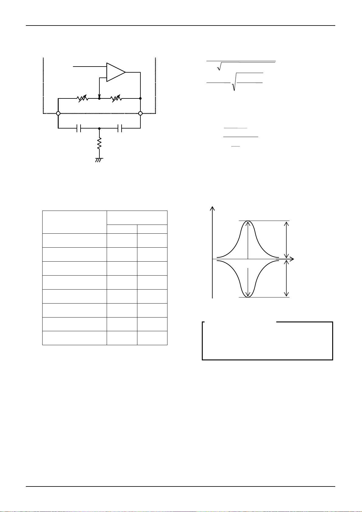
●Setting constants for tone control filters
1) Treble filter
IN
+
-
OUT
R1
R2
Pin 75,76
C
Standard values of R1, R2 (reference)
Treble Boost Amount
Resistance (K)
Cut Amount
R1 R2
Technical Note
1
fc= (Hz)
2πR2C
R1+R2+Zc
G = 20log (dB)
R2+Zc
1
Zc= (Ω)
jωC
G
*Typ.
3dB
0dB 0 20
±2dB 4.1 15.9
±4dB 7.3 12.7
±6dB 10.3 9.7
±8dB 12.3 7.7
±10dB 14.0 6.0
±12dB 15.4 4.6
±14dB 16.5 3.5
*The actual boost /cut amount may deviate from the standard values in some degree.
G
f
fc
G
3dB
Fig. 5
www.rohm.com
© 2010 ROHM Co., Ltd. All rights reserved.
13/17
2010.06 - Rev.A
BD3816K1,BD3817KS
2) Bass filter
IN
R3 R2
Pin72,74
C1 C2
Fig. 6
Standard values of R2, R3 (reference)
(R1=4.7KΩ,C1=C2=0.1µF)
Boost Amount
Cut Amount
0dB 0 39.5
+
-
R1
Resistance (K)
*Typ.
R2 R3
Pin71,73
fo =
=
Q
When C1=C2
≈
20logG
G
Technical Note
1
+
R3)C1C2 R1(R22π
C2C1
C1C2R2
+
R3R2
R1
R3
+
R1
+
2
(dB)
2
1
+
R1
(HZ)
G
±2dB 10.3 29.2
±4dB 18.4 21.1
±6dB 24.8 14.7
±8dB 29.9 9.6
±10dB 33.8
±12dB 36.9 2.6
±14dB 39.5 0
*The actual boost/cut amounts may deviate from
the standard values in some degree.
5.7
fo
f
G
Fig. 7
* Bass Filter Feature
To be able to set the f0 and Q factors of Bass
characteristics to desired values, part of the
Bass Filter is constructed of the external
components, shown in Fig.6
www.rohm.com
© 2010 ROHM Co., Ltd. All rights reserved.
14/17
2010.06 - Rev.A

BD3816K1,BD3817KS
p
●Reference data
25
20
15
10
5
0
-5
-10
-15
-20
CIRCUIT CURRENT (mA)
-25
0246 810
VCC
VEE
VCC,VEE(V)
Fig.8 Circuit Current - Voltage Supply
8
6
4
2
GAIN(dB)
0
-2
10 100 1000 10000 100000
FREQUENCY(Hz)
Fig.11 Input Gain - Frequency
20
15
10
5
0
GAIN(dB)
-5
-10
-15
-20
10 100 1000 10000 100000
Fig.14 Bass Gain - Frequency Fig.15 Treble Gain - Frequency
+14dB
-14dB
FREQUENCY(Hz)
10
1
0.1
0.01
THD+N(%)
0.001
0.0001
0.001 0.01 0.1 1 10
INPUT VOLTAGE(Vrms)
Fig.17 REC Total Harmonic
Distortion - Input Voltage
-14~+14dB,
2dB/ste
0~7dB
1dB/step
10
1
0.1
0.01
0.001
OUTPUT VOLTAGE(Vrms)
0.001 0. 01 0.1 1 10
INPUT VOLT AGE(Vrms)
Fig.9 Output Voltage - Input Voltage
18
16
14
12
10
8
6
GAIN(dB)
4
2
0
-2
10 100 1000 10000 100000
FREQUENCY (Hz)
Fig.12 Output Gain - Frequency
20
15
10
5
0
-5
GAIN(dB)
-10
-15
-20
GAIN(dB)
-1
-2
-14~+14dB,
2dB/step
10 100 1000 10000 100000
FREQUENCY(Hz)
2
1
0
10 100 1000 10000 100000
FREQUENCY(Hz)
+14dB
-14dB
Fig.18 REC Voltage Gain -
Frequency
0~17dB
1dB/step
Technical Note
10
1
0.1
0.01
THD+N(%)
0.001
0.0001
0.001 0.01 0.1 1 10
INPUT VOLTAGE(Vrms)
Fig.10 Total Harmonic Distortion -
Input Voltage
5.0
4.0
3.0
2.0
NOISE(μVrms)
1.0
0.0
Fig.13 Output Noise Voltage -
10
0.1
0.01
OUTPUT VOLTAGE(Vrms)
0.001
Fig.16 REC Output Voltage -
OUTPUT GAIN/TONE ON
OUTPUT GAIN ON
VOLUME DIRECT
0246810
VCC,VEE(V)
Power Supply Voltage
1
0.001 0.01 0.1 1 10
INPUT VOLTAGE(Vrms)
Input Voltage
www.rohm.com
© 2010 ROHM Co., Ltd. All rights reserved.
15/17
2010.06 - Rev.A

BD3816K1,BD3817KS
●Notes for use
1. Numbers and data in entries are representative design values and are not guaranteed values of the items.
2. Although ROHM is confident that the example application circuit reflects the best possible recommendations, be sure to
verify circuit characteristics for your particular application. Modification of constants for other externally connected circuits
may cause variations in both static and transient characteristics for external components as well as this Rohm IC. Allow
for sufficient margins when determining circuit constants.
3. Absolute maximum ratings
Use of the IC in excess of absolute maximum ratings, such as the applied voltage or operating temperature range (Topr),
may result in IC damage. Assumptions should not be made regarding the state of the IC (short mode or open mode)
when such damage is suffered. A physical safety measure, such as a fuse, should be implemented when using the IC at
times where the absolute maximum ratings may be exceeded.
4. VEE potential
Make the VEE pin voltage such that it is the lowest voltage even when operating below it. Actually confirm that the
voltage of each pin does not become a lower voltage than the VEE pin, including transient phenomena.
5. Thermal design
Perform thermal design, in which there are adequate margins, by taking into account the power dissipation (Pd) in actual
states of use.
6. Short circuit between terminals and erroneous mounting
Pay attention to the assembly Direction of the ICs. Wrong mounting Direction or shorts between terminals, GND, or other
components on the circuits, can damage the IC.
7. Operation in strong electromagnetic field
Using the ICs in a strong electromagnetic field can cause operation malfunction.
8. Operating Voltage Range and Operating Temperature Range
The circuit functional operations are guaranteed within the Operating Voltage Range and Operating Temperature Range.
The standard values of electrical characteristics, however, are guaranteed under the specific conditions. Accordingly,
careful consideration of the IC characteristic variations is required to design a set of circuit.
9. Power ON/OFF
(a) At power ON/OFF, a shock sound will be generated. Therefore, use MUTE on the set.
(b) When turning on power supplies, VEE and VCC should be powered on simultaneously, or VEE first followed by
VCC. If the VCC side is started up first, an excessive current may flow from VCC to VEE.
10. Serial control
For the CL and DA terminals, the patterned and other wirings should be routed as not to cause interference with
the analog-signal-related lines.
11. Function switching
For the all functions other than Master Volume, Treble, and Bass Gain Settings, use MUTE on the set.
Technical Note
www.rohm.com
© 2010 ROHM Co., Ltd. All rights reserved.
16/17
2010.06 - Rev.A

BD3816K1,BD3817KS
●Ordering part number
B D 3 8 1 6 K 1
Part No. Part No.
3816
3817
QFP80
65
24.0±0.3
20.0±0.2
4164
40
18.0±0.3
14.0±0.2
80
2.7±0.1
0.05
SQFP100
25
1
0.8
24.0±0.3
20.0±0.2
80
81
24
0.15
0.35±0.1
51
50
1.2
0.15±0.1
(Unit : mm)
14.0±0.2
18.0±0.3
100
1
31
30
1.2
0.15±0.1
Package
K1: QFP80
KS: SQFP100
<Tape and Reel information>
Tray (with dry pack)Container
Quantity
Direction of feed
1pin
<Tape and Reel information>
Quantity
Direction of feed
1pin
500pcs
Direction of product is fixed in a tray
Tray (with dry pack)Container
500pcs
Direction of product is fixed in a tray
Packaging and forming specification
None:Tray
Order quantity needs to be multiple of the minimum quantity.
∗
Technical Note
2.7±0.1
0.05
0.65
0.15
0.3±0.1
(Unit : mm)
Order quantity needs to be multiple of the minimum quantity.
∗
www.rohm.com
© 2010 ROHM Co., Ltd. All rights reserved.
17/17
2010.06 - Rev.A

Notes
No copying or reproduction of this document, in part or in whole, is permitted without the
consent of ROHM Co.,Ltd.
The content specied herein is subject to change for improvement without notice.
The content specied herein is for the purpose of introducing ROHM's products (hereinafter
"Products"). If you wish to use any such Product, please be sure to refer to the specications,
which can be obtained from ROHM upon request.
Examples of application circuits, circuit constants and any other information contained herein
illustrate the standard usage and operations of the Products. The peripheral conditions must
be taken into account when designing circuits for mass production.
Great care was taken in ensuring the accuracy of the information specied in this document.
However, should you incur any damage arising from any inaccuracy or misprint of such
information, ROHM shall bear no responsibility for such damage.
The technical information specied herein is intended only to show the typical functions of and
examples of application circuits for the Products. ROHM does not grant you, explicitly or
implicitly, any license to use or exercise intellectual property or other rights held by ROHM and
other parties. ROHM shall bear no responsibility whatsoever for any dispute arising from the
use of such technical information.
Notice
The Products specied in this document are intended to be used with general-use electronic
equipment or devices (such as audio visual equipment, ofce-automation equipment, communication devices, electronic appliances and amusement devices).
The Products specied in this document are not designed to be radiation tolerant.
While ROHM always makes effor ts to enhance the quality and reliability of its Products, a
Product may fail or malfunction for a variety of reasons.
Please be sure to implement in your equipment using the Products safety measures to guard
against the possibility of physical injury, re or any other damage caused in the event of the
failure of any Product, such as derating, redundancy, re control and fail-safe designs. ROHM
shall bear no responsibility whatsoever for your use of any Product outside of the prescribed
scope or not in accordance with the instruction manual.
The Products are not designed or manufactured to be used with any equipment, device or
system which requires an extremely high level of reliability the failure or malfunction of which
may result in a direct threat to human life or create a risk of human injury (such as a medical
instrument, transportation equipment, aerospace machinery, nuclear-reactor controller, fuelcontroller or other safety device). ROHM shall bear no responsibility in any way for use of any
of the Products for the above special purposes. If a Product is intended to be used for any
such special purpose, please contact a ROHM sales representative before purchasing.
If you intend to export or ship overseas any Product or technology specied herein that may
be controlled under the Foreign Exchange and the Foreign Trade Law, you will be required to
obtain a license or permit under the Law.
Thank you for your accessing to ROHM product informations.
More detail product informations and catalogs are available, please contact us.
ROHM Customer Support System
www.rohm.com
© 2010 ROHM Co., Ltd. All rights reserved.
http://www.rohm.com/contact/
R1010
A
 Loading...