

Page 1
Sound Processors for Home Theater Systems
6ch
Electronic Volume
BD3814FV
●Description
BD3814FV is a 1-chip sound processor incorporating such functions as volume, bass, and treble, necessary for AV receivers,
home theater systems, and mini-audio systems. This IC adopts the Bi-CMOS process, and realizes low distortion, low noise,
and a wide dynamic range.
●Features
1) Dynamic range: 132dB (tone bypath, VOL = MUTE, IHF-A)
2) Master volume 6ch independent (0 to -95dB, MUTE 1dB/step)
3) Low current consumption design achieved by adopting the BiCMOS process
4) Maximum output voltage: 4.3Vrms (Vcc=7V, VEE=-7V, RL=10kΩ)
5) Built-in 2 OP amplifiers
6) 2-line serial control (for both 3.3V and 5V)
●Applications
AV receivers, home theater systems, mini-audio systems, TVs etc.
●Absolute maximum ratings (Ta=25℃)
Parameter Symbol Ratings Unit
Power supply voltage
VCC 7.5*1
VEE -7.5
V
No.10081EAT05
Input signal voltage VIN VCC+0.3 to VEE-0.3 V
Power dissipation Pd 900*2 mW
Operating temperature range Topr -20 to +75 ℃
Storage temperature range Tastg -55 to +125 ℃
*1 Even in the specified range of Power Supply Voltage, applying voltage only to the VCC side may cause an excessive current
to give a permanent damage to the IC.
When starting up power supplies, VEE and VCC should be powered on simultaneously or VEE first; then followed by VCC.
*2 Reduced by 9 mW/C over 25C, when installed on the standard board (size: 70x70x1.6mm).
●Operating conditions
Must function normally at Ta=25℃.
Parameter Symbol
Operating source voltage
VCC 5 7 7.3
VEE -7.3 -7 -5
Ratings
Min. Typ. Max.
Unit
V
www.rohm.com
© 2010 ROHM Co., Ltd. All rights reserved.
1/10
2010.06 - Rev.A
Page 2
BD3814FV
●Electrical characteristics
Ta =2 5℃, VCC=7V, VEE=-7V, f=1kHz, Vin=1Vrms, RL=10kΩ, Rg=600Ω, Master volume=0dB,
Bass and Treble=0dB unless otherwise noted.
Circuit current
L input current(CL,DA) IIL ― 0.5 5 µA CL=DA=0V
H input current(CL,DA) IIH ― 0 5 µA CL=DA=5V
Output voltage gain 1 Gv1 -2 0 2 dB Measure: Pin27,28,29,30, 31,32
Output voltage gain 2 Gv2 -2 0 2 dB Measure: Pin3, 7
Parameter Symbol
VCC
IQ
VEE -17 -7 ―
Limits
Min. Typ. Max.
― 7 17
Unit. Conditions
mA No signal
Technical Note
Total harmonic distortion
ratio 1
Total harmonic distortion
ratio 2
Maximum output voltage 1 Vomax1 3.6 4.3 ― Vrms
Maximum output voltage 2 Vomax2 3.6 4.3 ― Vrms
Total output
Output noise voltage 1 Vno1
Output noise voltage 2 Vno2 ― 1.0 6.0 µVrms
Cross talk between channels
Rch→Lch
Cross talk between channels
Lch→Rch
Cross talk between channels
SRch→SLch
Cross talk between channels
SLch→SRch
Cross talk between channels
Cch→SWch
THD1 ― 0.001 0.03 %
THD2 ― 0.001 0.03 %
― 1.0 6.0 µVrms
― 1.7 10 µVrms
CTCRL ― -95 -80 dB
CTCLR ― -95 -80 dB
CTCSRL ― -95 -80 dB
CTCSLR ― -95 -80 dB
CTCCSW ― -95 -80 dB
Measure: Pin27,28,29,30,31,32
BW=400 ~ 30kHz
Measure: Pin3, 7
BW=400 ~ 30KHz
Measure: Pin27,28,29,30,31,32
THD=1%
Measure: Pin 3,7
THD=1%
Measure: Pin 27, 28
Tone: By-pass, Rg=0Ω, BW=IHF-A
Measure: Pin 27, 28
Tone: ON, Rg=0Ω, BW=IHF-A
Measure: Pin3, 7, 29, 30, 31, 32
Rg=0Ω, BW=IHF-A
Measure: Pin27(OUTFL)
Rg=0Ω, BW=IHF-A
Reference: Pin28(OUTFR)=1Vrms
Measure: Pin28(OUTFR)
Rg=0Ω, BW=IHF-A
Reference: Pin27(OUTFL)=1Vrms
Measure: Pin 30(OUTSL)
Rg=0Ω, BW=IHF-A
Reference: Pin31(OUTSR)=1Vrms
Measure: Pin 31(OUTSR)
Rg=0Ω, BW=IHF-A
Reference: Pin30(OUTSL)=1Vrms
Measure: Pin 32(OUTSW)
Rg=0Ω, BW=IHF-A
Reference: Pin29(OUTC) =1Vrms
www.rohm.com
© 2010 ROHM Co., Ltd. All rights reserved.
2/10
2010.06 - Rev.A
Page 3

BD3814FV
Input impedance V RinV 14 20 26 kΩ Measure: Pin27,28,29,30,31,32
Parameter Symbol
Min. Typ. Max.
Limits
Technical Note
Unit. Conditions
Volume control range GVR -98 -95 -92 dB
Volume set error 1 VE1 -1.5 0 1.5 dB
Volume set error 2 VE2 -2.5 0 2.5 dB
Maximum attenuation
amount
Volume output
Residual noise voltage 1 Vnom1 ― 1.0 6.0 µVrms
Residual noise voltage 2 Vnom2 ― 1.0 6.0 µVrms
Cross talk between channels
SWch→Cch
Treble maximum boost gain GTB 12 14 16 dB
Treble maximum cut gain GTC -16 -14 -12 dB
Vmin ― -115 -105 dB
CTCSWC ― -95 -80 dB
Measure: Pin27,28,29,30,31,32
Vin=3Vrms
Measure: Pin27,28,29,30, 31,32
0 to –53dB, Vin=3Vrms
Measure: Pin27,28,29,30,31,32
-54 to –95dB, Vin =3Vrms
Measure: Pin27,28,29,30,31,32
Vin =3Vrms, BW=IHF-A
Measure: Pin27, 28
Tone: By-Pass, Rg=0Ω, BW=IHF-A
Measure: Pin29, 30, 31, 32
Rg=0Ω, BW=IHF-A
Measure: Pin 29(OUTC)
Rg=0Ω, BW=IHF-A
Reference: Pin32(OUTSW)=1Vrms
Measure: Pin 27, 28
f=15kHz, Vin =0.4Vrms
Measure: Pin 27, 28
f=15kHz, Vin =0.4Vrms
Treble
Treble step resolution TR ― 2 ― dB
Treble gain set error TE -2 0 2 dB
Bass maximum boost gain GBB 12 14 16 dB
Bass maximum cut gain GBC -16 -14 -12 dB
Bass
Bass step resolution BR ― 2 ― dB
Bass gain set error BE -2 0 2 dB
* Note: This IC is not designed to be radiation-resistant.
Measure: Pin 27, 28
f=15kHz, Vin =0.4Vrms
Measure: Pin 27, 28
f=15kHz, Vin =0.4Vrms
Measure: Pin 27, 28
f=100Hz, Vin=0.4Vrms
Measure: Pin 27, 28
f=100Hz, Vin =0.4Vrms
Measure: Pin 27, 28
f=100Hz, Vin =0.4Vrms
Measure: Pin 27, 28
f=100Hz, Vin =0.4Vrms
www.rohm.com
© 2010 ROHM Co., Ltd. All rights reserved.
3/10
2010.06 - Rev.A
Page 4
BD3814FV
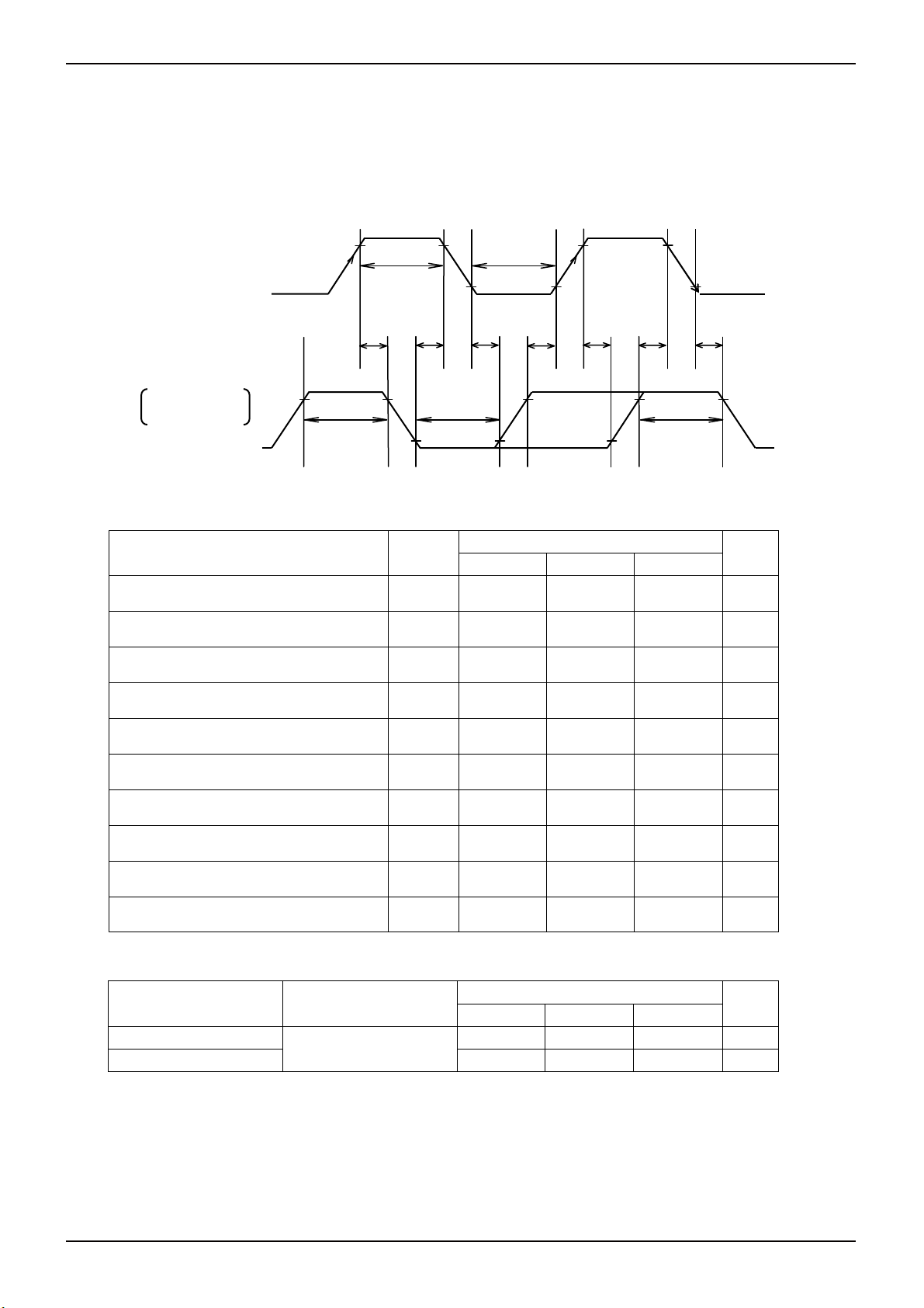
●Timing chart
1. Signal timing conditions
・Data is read on the rising edge of the clock.
・Latch is read on the falling edge of the clock.
・Latch signal must terminate with the LOW state.
* To avoid malfunctions, clock and data signals must terminate with the LOW state.
(CLOCK)
DATA
LATCH
CL
DA
90% 90% 90%
DATA DATA
Parameter Symbol
Technical Note
90% 90% 90% 90%
twc
10% 10% 10%
thd thdth ts tsl thl tsd
twd
twh
Fig.1
twc
90% 90%
twl
10%
10% 10%
LATCH
Limits
Min. Typ. Max.
Terminate
with Low.
Unit
Minimum clock width twc 2.0 - - μs
Minimum data width twd 2.0 - - μs
Minimum latch width twl 2.0 - - μs
LOW hold width twh 2.0 - - μs
Data setup time (DATA→CLK) tsd 1.0 - - μs
Data hold time (CLK→DATA) thd 1.0 - - μs
Latch setup time (CLK→LATCH) tsl 1.0 - - μs
Latch hold time (DATA→LATCH) thl 1.0 - - μs
Latch low setup time ts 1.0 - - μs
Latch low hold time th 1.0 - - μs
2. Voltage conditions for control signal
Parameter
“H” input voltage
“L” input voltage 0 - 1.0 V
Condition
Vcc=5 ~ 7.3V
VEE=-5 ~ -7.3V
Limits
Min. Typ. Max.(≦Vcc)
Unit
2.2 - 5.5 V
www.rohm.com
© 2010 ROHM Co., Ltd. All rights reserved.
4/10
2010.06 - Rev.A
Page 5

BD3814FV
3. Basic configuration of control data format
Data input direction
MSB LSB
D16 D15 D14 D13 D12 D11 D10 D9 D8 D7 D6 D5 D4 D3 D2 D1 D0
Data
・Control data format
Data input direction
D16 D15 D14 D13 D12 D11 D10 D9 D8 D7 D6 D5 D4 D3 D2 D1 D0
Data
①
D16 D15 D14 D13 D12 D11 D10 D9 D8 D7 D6 D5 D4 D3 D2 D1 D0
Data
②
D16 D15 D14 D13 D12 D11 D10 D9 D8 D7 D6 D5 D4 D3 D2 D1 D0
Data
③
D16 D15 D14 D13 D12 D11 D10 D9 D8 D7 D6 D5 D4 D3 D2 D1 D0
Data
④
Treble Bass Tone * * * * * 0 0 0
Master Volume FRch Master Volume FLch 0 0 1
Master Volume SRch Master Volume SLch 0 1 0
Master Volume Cch Master Volume SWch 0 1 1
Technical Note
Data Select Address
Select Address
By changing select address, 4 control data formats can be selected.
Do not set the select address data to any format other than that specified above.
At power-on sequence, initialize all data.
* is 0 or 1.
Example:
Data input direction
MSB LSB MSB LSB MSB LSB MSB LSB
Data① L Data② L Data③ LData④ L
“L” shows latch.
After power-on, for the second and subsequent times, only the necessary data can be selected for setting
Example: When to change bus,
Input direction
MSB LSB
Data① L
“L” shows latch.
www.rohm.com
© 2010 ROHM Co., Ltd. All rights reserved.
5/10
2010.06 - Rev.A
Page 6

BD3814FV
●Application circuit
47K
47K
IN
SW
IN
SR
IN
SL
IN
C
IN
FR
IN
FL
VEE
47
1
2
3
4
5
6
7
8
9
µ
10
10
11
µ
10
12
13
µ
10
14
15
µ
10
16
17
µ
10
18
19
µ
10
20
µ
MASTER
VOLUME
0~-95dB
1dB/step,MUTE
Ri=20K
Ri=20K
Ri=20K
Ri=20K
Ri=20K
Ri=20K
Fig.2
BASS
TREBLE
Technical Note
40
39
47
38
10K
37
10K
36
10K
35
34
33
32
31
30
29
28
27
0.1
26
25
0.1
0.1
24
23
0.1
22
4700P
21
4700P
UNIT
RESISTOR: Ω
CAPACITOR: F
µ
µ
µ
µ
µ
Vcc
CL
DA
MUTE
OUTSW
OUTSR
OUTSL
OUTC
OUTFR
OUTFL
4.7K
4.7K
www.rohm.com
© 2010 ROHM Co., Ltd. All rights reserved.
6/10
2010.06 - Rev.A
Page 7

BD3814FV
●Reference data
8
6
4
2
0
-2
-4
CIRCUIT CURRENT (mA)
-6
-8
0510
POW ER SUPPL Y (V)
Fig.3 Circuit current - Power supply
10
1
0.1
0.01
THD+N (%)
0.001
0.0001
0.001 0.01 0.1 1 10
INPUT VOLTAGE (Vrms)
Fig.6 THD+N - Input voltage
VCC
VEE
10
8
6
4
2
0
-2
GAIN (dB)
-4
-6
-8
-10
10 100 1000 10000 100000
FREQUENCY (Hz)
Fig.4 Voltage gain - Frequency
20
15
10
GAIN (dB)
-5
-10
-15
-20
+14dB
5
0
10 100 1000 10000 100000
-14~+14dB
2dB/step
-14dB
FREQUENCY (Hz)
Fig.7 Bass gain - Frequency
Technical Note
10
1
0.1
0.01
OUTPUT VOLTAGE (Vrms )
0.001
0.001 0.01 0.1 1 10
IN PUT VOLTAGE (Vrms)
Fig.5 Output voltage - Input voltage
20
15
10
5
0
-5
GAIN (dB)
-14~+14dB
-10
-15
-20
2dB/step
10 100 1000 10000 100000
FREQUENCY (Hz)
Fig.8 Treble gain - Frequency
+14dB
-14dB
www.rohm.com
© 2010 ROHM Co., Ltd. All rights reserved.
7/10
2010.06 - Rev.A
Page 8

BD3814FV
●Notes for use
1. Numbers and data in entries are representative design values and are not guaranteed values of the items.
2. Although ROHM is confident that the example application circuit reflects the best possible recommendations, be sure to
verify circuit characteristics for your particular application. Modification of constants for other externally connected circuits
may cause variations in both static and transient characteristics for external components as well as this Rohm IC. Allow for
sufficient margins when determining circuit constants.
3. Absolute maximum ratings
Use of the IC in excess of absolute maximum ratings, such as the applied voltage or operating temperature range (Topr),
may result in IC damage. Assumptions should not be made regarding the state of the IC (short mode or open mode) when
such damage is suffered. A physical safety measure, such as a fuse, should be implemented when using the IC at times
where the absolute maximum ratings may be exceeded.
4. VEE potential
Make the VEE pin voltage such that it is the lowest voltage even when operating below it. Actually confirm that the
voltage of each pin does not become a lower voltage than the VEE pin, including transient phenomena.
5. Thermal design
Perform thermal design, in which there are adequate margins, by taking into account the power dissipation (Pd) in actual
states of use.
6. Short circuit between terminals and erroneous mounting
Pay attention to the assembly direction of the ICs. Wrong mounting direction or shorts between terminals, GND, or other
components on the circuits, can damage the IC.
Technical Note
7. Operation in strong electromagnetic field
Using the ICs in a strong electromagnetic field can cause operation malfunction.
8. Serial control
For the CL and DA terminals, the patterned and other wirings should be routed as not to cause interference with the
analog-signal-related lines.
9. Power ON/OFF
(a) At power ON/OFF, a shock sound will be generated. Therefore, use MUTE on the set.
(b) When turning on power supplies, VEE and VCC should be powered on simultaneously, or VEE first followed
by VCC. If the VCC side is started up first, an excessive current may flow from VCC to VEE.
10. Tone bypath switching
For tone bypath switching, use MUTE on the set.
www.rohm.com
© 2010 ROHM Co., Ltd. All rights reserved.
8/10
2010.06 - Rev.A
Page 9

BD3814FV
●Thermal derating characteristic
1000
800
600
400
Power Diss ipation Pd (mW)
200
0
BD3814FV
ROHM standard board packaging time value
Board size: 70 x 70 x 1.6mm Raw material : FR4 glass epoxy board (copper area 3% or below)
Technical Note
900mW
0 25 50 75 100 125
Ta(℃)
Fig.9
www.rohm.com
© 2010 ROHM Co., Ltd. All rights reserved.
9/10
2010.06 - Rev.A
Page 10

BD3814FV
●Ordering part number
B D 3 8 1 4 F V - E 2
Part No. Part No.
SSOP-B40
13.6 ± 0.2
(MAX 13.95 include BURR)
40
21
5.4 ± 0.2
7.8 ± 0.3
1
20
0.5 ± 0.2
0.15 ± 0.1
1.8 ± 0.1
0.1
0.65
0.22 ± 0.1
0.08
0.1 S
M
(Unit : mm)
Package
FV: SSOP-B40
<Tape and Reel information>
Embossed carrier tapeTape
Quantity
Direction
of feed
2000pcs
E2
The direction is the 1pin of product is at the upper left when you hold
()
reel on the left hand and you pull out the tape on the right hand
Reel
Packaging and forming specification
E2: Embossed tape and reel
1pin
Order quantity needs to be multiple of the minimum quantity.
∗
Technical Note
Direction of feed
www.rohm.com
© 2010 ROHM Co., Ltd. All rights reserved.
10/10
2010.06 - Rev.A
Page 11

Notes
No copying or reproduction of this document, in part or in whole, is permitted without the
consent of ROHM Co.,Ltd.
The content specied herein is subject to change for improvement without notice.
The content specied herein is for the purpose of introducing ROHM's products (hereinafter
"Products"). If you wish to use any such Product, please be sure to refer to the specications,
which can be obtained from ROHM upon request.
Examples of application circuits, circuit constants and any other information contained herein
illustrate the standard usage and operations of the Products. The peripheral conditions must
be taken into account when designing circuits for mass production.
Great care was taken in ensuring the accuracy of the information specied in this document.
However, should you incur any damage arising from any inaccuracy or misprint of such
information, ROHM shall bear no responsibility for such damage.
The technical information specied herein is intended only to show the typical functions of and
examples of application circuits for the Products. ROHM does not grant you, explicitly or
implicitly, any license to use or exercise intellectual property or other rights held by ROHM and
other parties. ROHM shall bear no responsibility whatsoever for any dispute arising from the
use of such technical information.
Notice
The Products specied in this document are intended to be used with general-use electronic
equipment or devices (such as audio visual equipment, ofce-automation equipment, communication devices, electronic appliances and amusement devices).
The Products specied in this document are not designed to be radiation tolerant.
While ROHM always makes efforts to enhance the quality and reliability of its Products, a
Product may fail or malfunction for a variety of reasons.
Please be sure to implement in your equipment using the Products safety measures to guard
against the possibility of physical injury, re or any other damage caused in the event of the
failure of any Product, such as derating, redundancy, re control and fail-safe designs. ROHM
shall bear no responsibility whatsoever for your use of any Product outside of the prescribed
scope or not in accordance with the instruction manual.
The Products are not designed or manufactured to be used with any equipment, device or
system which requires an extremely high level of reliability the failure or malfunction of which
may result in a direct threat to human life or create a risk of human injury (such as a medical
instrument, transportation equipment, aerospace machinery, nuclear-reactor controller, fuelcontroller or other safety device). ROHM shall bear no responsibility in any way for use of any
of the Products for the above special purposes. If a Product is intended to be used for any
such special purpose, please contact a ROHM sales representative before purchasing.
If you intend to export or ship overseas any Product or technology specied herein that may
be controlled under the Foreign Exchange and the Foreign Trade Law, you will be required to
obtain a license or permit under the Law.
Thank you for your accessing to ROHM product informations.
More detail product informations and catalogs are available, please contact us.
ROHM Customer Support System
www.rohm.com
© 2010 ROHM Co., Ltd. All rights reserved.
http://www.rohm.com/contact/
R1010
A
 Loading...