

Page 1
*
1
Sound Processors for Home Theater Systems
2ch
Electronic Volume
BD3812F
●Description
BD3812F is an electronic volume having volume, gain amplifier functions necessary for applications in AV receivers, home
theatre systems, min-component systems and so forth. Having a chip select terminal, it can be controlled until 4 chips with
common bus line.
●Features
1) Residual noise : 1.2µVrms {dynamic range : 131dB (IHF-A)}
2) 2ch independent volume (0 to -103dB, MUTE 1dB/step)
3) 8ch at maximum available in combination of any of BD3811K1, BD3813KS, BD3814FV, BD3815KS (6ch volume)
in common bus line
4) It can be controlled until 4 chips with common bus line at the same time
5) Maximum output voltage : 4.2Vrms (Vcc=7, VEE=-7V, RL=10kΩ)
6) 2-line serial control (for both 3.3V and 5V)
7) Built-in Output gain amplifier for adjustment of output signal voltage (0, 6 to 18dB, 2dB/step)
8) Output mute controllable by serial data and external control terminal
●Applications
AV receivers, home theater systems, mini-component systems, etc.
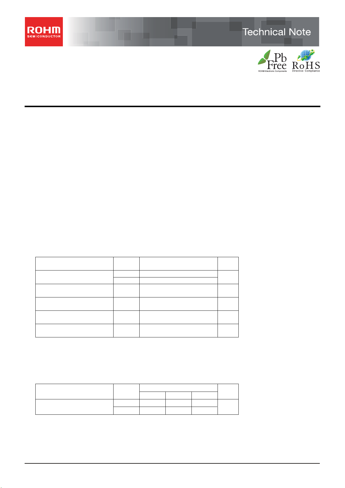
●Absolute maximum ratings (Ta=25℃)
Parameter Symbol Ratings Unit
No.10081EAT03
Powewr supply voltage
Input signal voltage VIN VCC+0.3 to VEE-0.3 V
Power dissipation Pd 450*2 mW
Operating temperature range Topr -20 to +75 ℃
Storage temperature range Tastg -55 to +125 ℃
*1 Even in the specified range of Power Supply Voltage, applying voltage only to the VCC side may
cause an excessive current to give a permanent damage to the IC.
When starting up power supplies, VEE and VCC should be powered on simultaneously or VEE first; then followed by VCC.
*2 Over Ta=25°C, reduce at the rate of 4.5mW/°C. When installed on the standard board (size: 70x70x1.6mm).
●Operating conditions
It must function normally at Ta=25°C.
Parameter Symbol
Operating source voltage
VCC 7.5
VEE -7.5
Min. Typ. Max.
VCC 5 7 7.3
VEE -7.3 -7 -5
Ratings
V
Unit
V
www.rohm.com
© 2010 ROHM Co., Ltd. All rights reserved.
1/9
2010.06 - Rev.A
Page 2
BD3812F
●Electrical characteristics
Ta =2 5℃, VCC=7V, VEE=-7V, f=1kHz, Vin=1Vrms, RL=10kΩ, Rg=600Ω, Master volume=0dB, Output gain=0dB , unless
otherwise specified.
Parameter
VCC
Circuit current
VEE -6 -2 ―
Output voltage gain Gv -2 0 2 dB Measure : Pin14, 13
Symbol
IQ
Min. Typ. Max.
Limits
― 2 6
Unit Conditions
mA No signal
Technical Note
Total harmonic distortion ratio THD ― 0.005 0.09 %
Maximum output voltage Vomax 3.4 4.2 ― Vrms
Output noise voltage Vno ― 1.2 5 µVrms
Input impedance Rin 20 30 40 kΩ Measure : Pin1, 3
Cross talk between channels
1ch→2ch
Cross talk between channels
2ch→1ch
Volume control range GVR -106 -103 -100 dB
Volume set error 1 VE1 -2 0 2 dB
Volume set error 2 VE2 -3 0 3 dB
CTC12 ― -100 -70 dB
CTC21 ― -100 -70 dB
Measure : Pin14, 13
BW=400~30kHz
Measure : Pin14, 13
THD=1%
Measure : Pin 14, 13
Rg=0Ω, BW=IHF-A
Measure : Pin13(OUT2)
Rg=0Ω, BW=IHF-A
Reference : Pin14(OUT1)=1Vrms
Measure : Pin14(OUT1)
Rg=0Ω, BW=IHF-A
Reference : Pin13(OUT2)=1Vrms
Measure : Pin 14, 13
Vin=3Vrms
Measure : Pin 14, 13
0 to –53dB, Vin=3Vrms
Measure : Pin 14, 13
-54 to –103dB, Vin=3Vrms
Maximum attenuation Vmin ― -118 -105 dB
Output gain control range GOG 16 18 20 dB
Output gain set error GOE -2 0 -2 dB
* This product is not of “anti radiation design”.
Measure : Pin 14, 13
BW=IHF-A, Vin=3Vrms
Measure : Pin 14, 13
Vin=0.4Vrms
Measure : Pin 14, 13
Vin=0.4Vrms
www.rohm.com
© 2010 ROHM Co., Ltd. All rights reserved.
2/9
2010.06 - Rev.A
Page 3
BD3812F
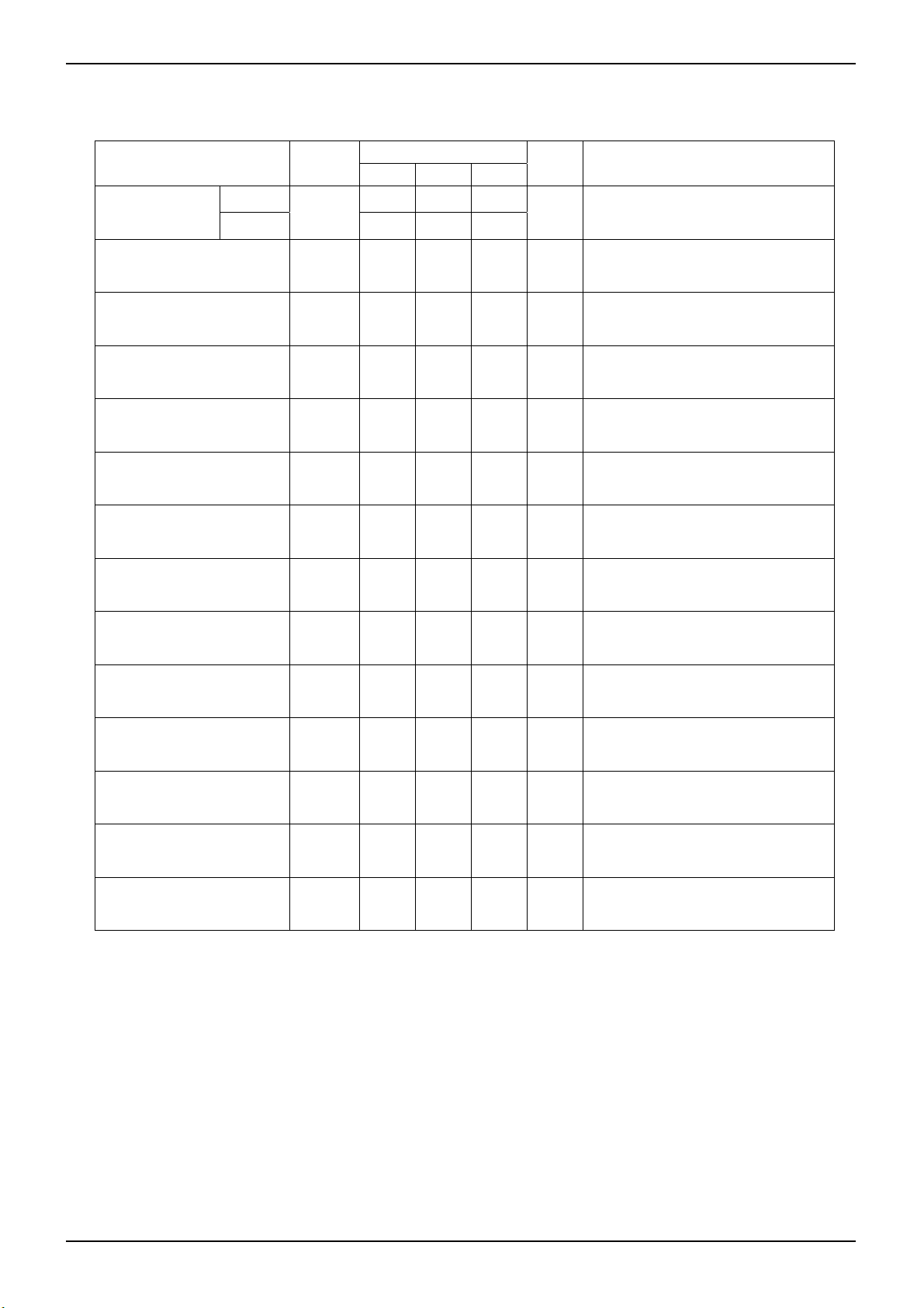
●Timing chart
1) Signal timing conditions
・Data is read on the rising edge of the clock.
・Latch is read on the falling edge of the clock.
・Latch signal must terminate with the LOW state.
* To avoid malfunctions, clock and data signals must terminate with the LOW state.
CL
(CLOCK)
90% 90% 90% 90%
twc
twc
10% 10% 10%
thd thdth ts tsl thl tsd
DA
DATA
LATCH
90% 90% 90%
twd
DATA DATA
twh
10%
Fig.1
Parameter Symbol
Min. Typ. Max.
90% 90%
twl
LATCH
10% 10%
Limits
Te rm in at e
with Low.
Technical Note
Unit
Minimum clock width twc 2.0 - - µs
Minimum data width twd 2.0 - - µs
Minimum latch width twl 2.0 - - µs
LOW hold width twh 2.0 - - µs
Data setup time
(DATA→CLK)
Data hold time(CLK→DATA) thd 1.0 - - µs
Latch setup time(CLK→LATCH) tsl 1.0 - - µs
Latch hold time(DATA→LATCH) thl 1.0 - - µs
Latch low setup time ts 1.0 - - µs
Latch low hold time th 1.0 - - µs
2) Voltage conditions for control signal
Parameter Condition
“H”input voltage
“L” input voltage 0 - 1.0 V
Vcc=5~7.3V
VEE=-5~-7.3V
tsd 1.0 - - µs
Limits
Min. Typ. Max.(≦Vcc)
Unit
2.2 - 5.5 V
www.rohm.com
© 2010 ROHM Co., Ltd. All rights reserved.
3/9
2010.06 - Rev.A
Page 4

BD3812F
3) Basic configuration of control data format
Input direction
MSB LSB
D16 D15 D14 D13 D12 D11 D10 D9 D8 D7 D6 D5 D4 D3 D2 D1 D0
Data
・Control data format
Input direction
D16 D15 D14 D13 D12 D11 D10 D9 D8 D7 D6 D5 D4 D3 D2 D1 D0
Data
①
D16 D15 D14 D13 D12 D11 D10 D9 D8 D7 D6 D5 D4 D3 D2 D1 D0
Data
②
* * * * * * * * * * * Output gain amp 1 1 1
* is 0 or 1.
By changing the setting of select address, 4 control data formats can be selected.
Do not set the select address data to other than specified above.
At power on, initialize all the data.
Input direction
Master Volume 2ch Master Volume 1ch 1 1 0
MSB LSB MSB LSB
Data Select Address
Technical Note
Select Address
Data① LData② L
After power on, in the second time or after, only data you want to change can be set.
(Example) When to change bus
“L” shows latch.
Input direction
MSB LSB
Data① L
“L” shows latch.
www.rohm.com
© 2010 ROHM Co., Ltd. All rights reserved.
4/9
2010.06 - Rev.A
Page 5

BD3812F
4) SEL terminal setting
By determining the SEL terminal voltage, select address can be fixed.
An example of the SEL terminal voltage setting method is shown below.
Technical Note
Setting
P1
Condition
Setting 1 VEE
P2
Condition
-
Setting 2 VCC VEE
Setting 3 VCC VEE
Setting of
SEL(12pin) Terminal
P1
20k
VEE
P1
P2
12
12
10k
10k
12
P1
P2
20k
VCC
VEE
VCC
VEE
SEL(12pin)
Terminal Voltage(V)
Select Address
D2 D1
VEE 0 0
VCC/3+2×VEE/3 0 1
VCC/3 1 0
P1
Setting 4 VCC -
12
VCC
VCC 1 1
SEL terminal voltage is DGND standard.
When to use several chips of BD3812F
Select address can be changed by setting SEL terminal (12pin), therefore, up to 4 chips can be used on a same bus line.
When to use one chip or two chips of this IC, use the setting 1 and the setting 4. In this case, the terminal voltage of 12pin
may be VCC or VEE, therefore external resistor of 12pin is unnecessary.
When to use BD3812F and BD3811K1 at the same time
By using BD3812F and BD3811K1 at the same time, independent control of 8ch volume can be made. And control is
available on a same bus line. In this case, be sure to set the SEL terminal setting to “setting 4”.
www.rohm.com
© 2010 ROHM Co., Ltd. All rights reserved.
5/9
2010.06 - Rev.A
Page 6

BD3812F
●Application circuit
IN1
10µ
1
AGND
2
IN2
3
10μ
AGND
4
VEE
AGND
VCC
5
47μ
6
47µ
7
●Reference data
2.5
2
1.5
1
0.5
0
-0.5
-1
-1.5
-2
CIRCUIT CURRENT (mA)
-2.5
024 6810
POWER SU PPLY (V)
Fig.3 Circuit current - Power supply
VCC
VEE
10
1
0.1
0.01
THD+N (%)
0.001
0.0001
0.001 0.01 0.1 1 10
INPUT VOLTAGE (Vrms)
Fig.6 THD+N - Input voltage
LOGIC
Fig.2
10
8
6
4
2
0
-2
GAIN(dB)
-4
-6
-8
-10
10 100 1000 10000 100000
FREQUENCY (Hz)
Fig.4 Voltage gain - Frequency
20
15
10
5
GAIN (dB)
0
-5
10 100 1000 10000 100000
FREQUENCY (Hz)
Fig.7 Output gain - Frequency
0, 6~18dB
2dB/step
Technical Note
14
13
12
11
10
9
8
UNIT
RESISTOR :Ω
CAPACITOR : F
10
1
0.1
0.01
OUTPUT VOLTAGE (Vrms )
0.001
0.001 0.01 0.1 1 10
INPUT VOLTAGE (Vrms)
Fig.5 Output voltage - Input voltage
OUT1
OUT2
SEL
DGND
MUTE
DA
CL
www.rohm.com
© 2010 ROHM Co., Ltd. All rights reserved.
6/9
2010.06 - Rev.A
Page 7

BD3812F
●Notes for use
(1) Numbers and data in entries are representative design values and are not guaranteed values of the items.
(2) Although we are confident in recommending the sample application circuits, carefully check their characteristics further
when using them. When modifying externally attached component constants before use, determine them so that they
have sufficient margins by taking into account variations in externally attached components and the Rohm LSI, not only for
static characteristics but also including transient characteristics.
(3) Absolute maximum ratings
If applied voltage, operating temperature range, or other absolute maximum ratings are exceeded, the LSI may be
damaged. Do not apply voltages or temperatures that exceed the absolute maximum ratings. If you think of a case in
which absolute maximum ratings are exceeded, enforce fuses or other physical safety measures and investigate how not
to apply the conditions under which absolute maximum ratings are exceeded to the LSI.
(4) VEE potential
Make the VEE pin voltage such that it is the lowest voltage even when operating below it. Actually confirm that the
voltage of each pin does not become a lower voltage than the VEE pin, including transient phenomena.
(5) Thermal design
Perform thermal design in which there are adequate margins by taking into account the allowable power dissipation in
actual states of use.
(6) Shorts between pins and misinstallation
When mounting the LSI on a board, pay adequate attention to orientation and placement discrepancies of the LSI. If it is
misinstalled and the power is turned on, the LSI may be damaged. It also may be damaged if it is shorted by a foreign
substance coming between pins of the LSI or between a pin and a power supply or a pin and a GND.
(7) Operation in strong magnetic fields
Adequately evaluate use in a strong magnetic field, since there is a possibility of malfunction.
(8) Serial control
For the CL and DA terminals, the patterned and other wirings should be routed not to cause interference with the
analog-signal-related lines.
(9) About power ON/OFF
(a) At power ON/OFF, a shock sound will be generated and, therefore, use MUTE on the set.
(b) When turning on power supplies, VEE and VCC should be powered on simultaneously or VEE first;
then followed by VCC. If the VCC side is started up first, an excessive current may pass VCC through VEE.
(10) Function switching
For the functions except master volume, use MUTE on the set.
(11) Reduction of switching noise when changing volume from -3dB to -4dB
In order to reduce switching noise when changing volume from -3dB to -4dB, after switching the switch of -4dB step,
change the switch of -1dB step by -1dB.
Technical Note
www.rohm.com
© 2010 ROHM Co., Ltd. All rights reserved.
7/9
2010.06 - Rev.A
Page 8

BD3812F
●Thermal derating characteristic
500
400
300
200
Power Dissipation Pd (mW)
100
0
BD3812
ROHM standard board packaging time value
Board size : 70 x 70 x 1.6mm Raw material : FR4 glass epoxy board (copper area 3% or below)
Technical Note
450mW
0 25 50 75 100 125
Ta(℃)
Fig.8
www.rohm.com
© 2010 ROHM Co., Ltd. All rights reserved.
8/9
2010.06 - Rev.A
Page 9
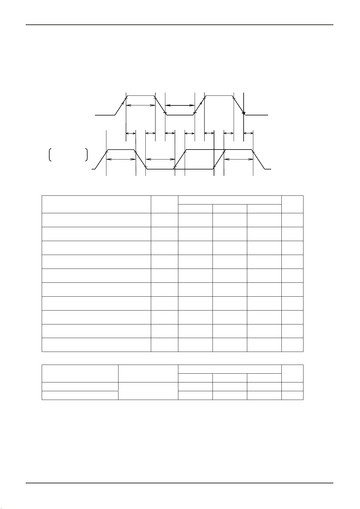
BD3812F
●Ordering part number
B D 3 8 1 2 F - E 2
Part No. Part No.
SOP14
(MAX 9.05 include BURR)
14
6.2± 0.3
4.4± 0.2
1
1.5± 0.1
1.27
0.11
8.7± 0.2
0.4± 0.1
8
0.3MIN
7
0.15± 0.1
0.1
(Unit : mm)
Package
F:SOP14
Packaging and forming specification
E2: Embossed tape and reel
<Tape and Reel information>
Embossed carrier tapeTape
Quantity
Direction
of feed
2500pcs
E2
The direction is the 1pin of product is at the upper left when you hold
()
reel on the left hand and you pull out the tape on the right hand
Reel
1pin
Order quantity needs to be multiple of the minimum quantity.
∗
Technical Note
Direction of feed
www.rohm.com
© 2010 ROHM Co., Ltd. All rights reserved.
9/9
2010.06 - Rev.A
Page 10

Notes
No copying or reproduction of this document, in part or in whole, is permitted without the
consent of ROHM Co.,Ltd.
The content specied herein is subject to change for improvement without notice.
The content specied herein is for the purpose of introducing ROHM's products (hereinafter
"Products"). If you wish to use any such Product, please be sure to refer to the specications,
which can be obtained from ROHM upon request.
Examples of application circuits, circuit constants and any other information contained herein
illustrate the standard usage and operations of the Products. The peripheral conditions must
be taken into account when designing circuits for mass production.
Great care was taken in ensuring the accuracy of the information specied in this document.
However, should you incur any damage arising from any inaccuracy or misprint of such
information, ROHM shall bear no responsibility for such damage.
The technical information specied herein is intended only to show the typical functions of and
examples of application circuits for the Products. ROHM does not grant you, explicitly or
implicitly, any license to use or exercise intellectual property or other rights held by ROHM and
other parties. ROHM shall bear no responsibility whatsoever for any dispute arising from the
use of such technical information.
Notice
The Products specied in this document are intended to be used with general-use electronic
equipment or devices (such as audio visual equipment, ofce-automation equipment, communication devices, electronic appliances and amusement devices).
The Products specied in this document are not designed to be radiation tolerant.
While ROHM always makes efforts to enhance the quality and reliability of its Products, a
Product may fail or malfunction for a variety of reasons.
Please be sure to implement in your equipment using the Products safety measures to guard
against the possibility of physical injury, re or any other damage caused in the event of the
failure of any Product, such as derating, redundancy, re control and fail-safe designs. ROHM
shall bear no responsibility whatsoever for your use of any Product outside of the prescribed
scope or not in accordance with the instruction manual.
The Products are not designed or manufactured to be used with any equipment, device or
system which requires an extremely high level of reliability the failure or malfunction of which
may result in a direct threat to human life or create a risk of human injury (such as a medical
instrument, transportation equipment, aerospace machinery, nuclear-reactor controller, fuelcontroller or other safety device). ROHM shall bear no responsibility in any way for use of any
of the Products for the above special purposes. If a Product is intended to be used for any
such special purpose, please contact a ROHM sales representative before purchasing.
If you intend to export or ship overseas any Product or technology specied herein that may
be controlled under the Foreign Exchange and the Foreign Trade Law, you will be required to
obtain a license or permit under the Law.
Thank you for your accessing to ROHM product informations.
More detail product informations and catalogs are available, please contact us.
ROHM Customer Support System
www.rohm.com
© 2010 ROHM Co., Ltd. All rights reserved.
http://www.rohm.com/contact/
R1010
A
 Loading...