

Page 1
1/4
Structure
: Silicon Monolithic Integrated Circuit
Product: Sound Processor for car audio
Type:
BD37541FS
Package: SSOP-A32
●Feature
1. Reduce switching noise of input gain control, mute, main volume, fader volume, bass, middle, treble, loudness,
by using advanced switch circuit [Possible to control all steps]
2. Built-in ground isolation amplifier inputs, ideal for external stereo input.
3. Built-in differential input selector that can make various combination of single-ended / differential input.
4. Built-in input gain controller reduce switching noise for volume of a portable audio input.
5. Decrease the number of external components by built-in 3-band equalizer fi lter.
And, possible to control Q, Gv, fo of 3-band equalizer by I
6. It is possible for the bass, middle, treble to the gain adjustment quantity of ±20dB and 1 dB step gain adjustment.
7. It is equipped with output terminals of Subwoofer. Moreover, the stereo signal of the front and rear also can be
output by the I
2
C BUS control.
8. Built-in mixing input.
9. Bi-CMOS process is suitable for the design of low current and low energy. And it provides more quality for
small-scale regulator and heat in a set.
10. Package is SSOP-A32. Putting input-terminals together and output-terminals together can make PCB layout
easier and can makes area of PCB smaller.
11. It is possible to control by 3.3V / 5V for I
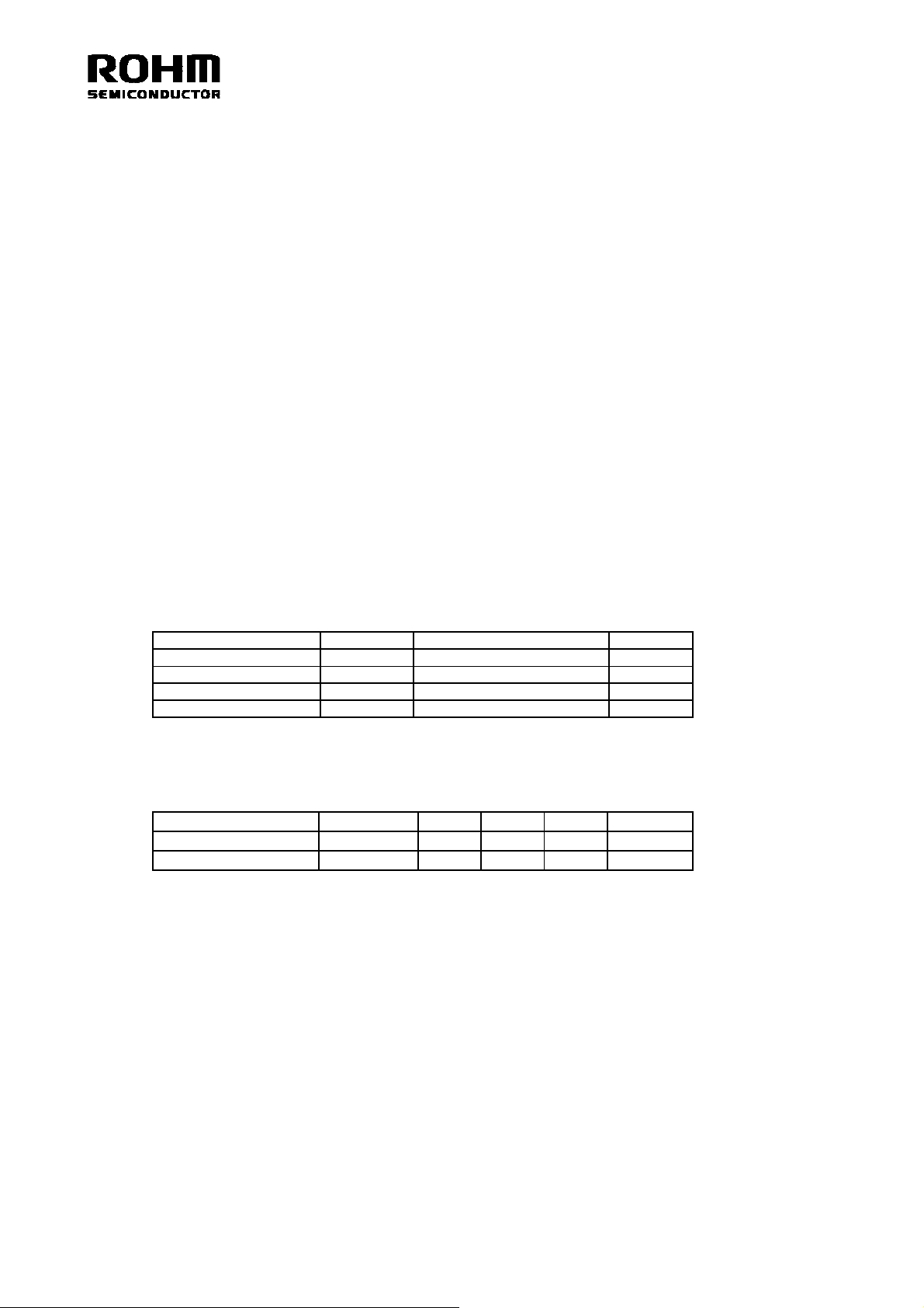
●Absolute Maximum Ratings (Ta=25℃)
Parameter Symbol Limits Unit
Power supply Voltage VCC 10.0 V
Input voltage VIN VCC+0.3~GND-0.3 V
Power Dissipation Pd 950 ※1mW
Storage Temperature T astg -55~+150 ℃
※1 At T a=25°C or higher, this value is decreaced to 8.5mW/°C
When Rohm standard board is mounted.
Rohm standard board:
Size:70×70×1.6(mm3)
material:FR4 glass-epoxy substrate (copper foil area: not more than 3%).
●Operating Range
Parameter Symbol Min. Typ. Max. Unit
Power supply Voltage VCC 7.0 - 9.5 V
Temperature Topr -40 - +85 ℃
※Design against radiation-proof isn’t made.
2
C BUS.
2
C BUS control freely.
REV . A
Page 2
2/4
2
)
X
g(
)
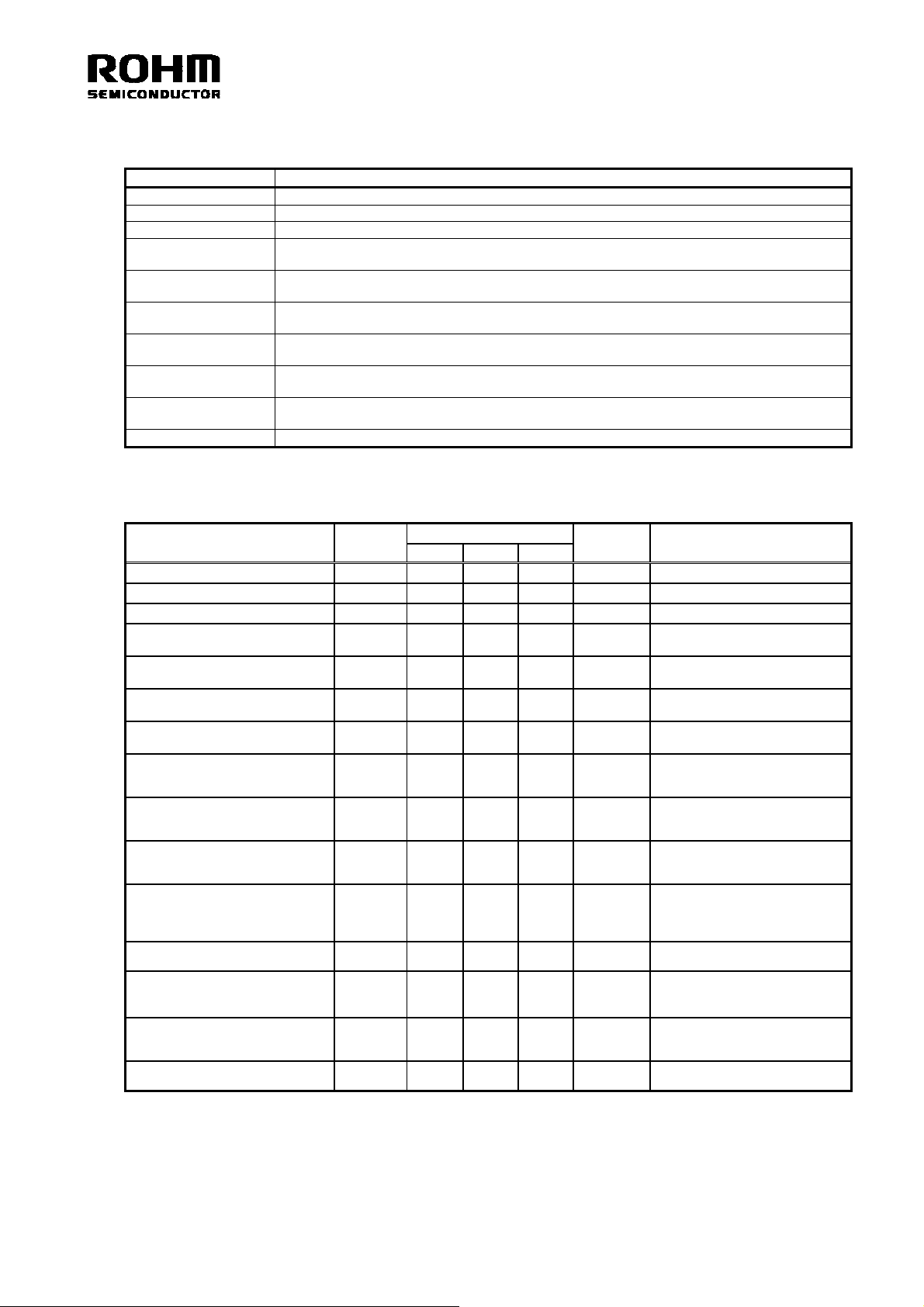
●Function
Function Specifications
Input selector
Input gain
Mute
Volume
Bass
Middle
Treble
Fader
Loudness
Mixing Monaural input
Stereo 3 single-end input and 2differential input possible to switch single-end input
0~20dB (1dB step), Possible to use “Advanced switch” for prevention of switching noise.
Possible to use “Advanced switch” for prevention of switching noise.
+15dB~-79dB (1dB step), -∞dB
Possible to use “Advanced switch” for prevention of switching noise.
-20~+20dB (1dB step), Q=0.5, 1, 1.5, 2, fo=60, 80, 100, 120Hz
Possible to use advanced switch at changing gain
-20~+20dB (1dB step), Q=0.75, 1, 1.25, 1.5, fo=500, 1k, 1.5k, 2.5kHz
Possible to use advanced switch at changing gain
-20~+20dB (1dB step), Q=0.75, 1.25, fo=7.5k, 10k, 12.5k, 15kHz
Possible to use advanced switch at changing gain
0dB~-79dB (1dB step), -∞dB
Possible to use “Advanced switch” for prevention of switching noise.
0dB~20dB (1dB step)
Possible to use “Advanced switch” for prevention of switching noise.
●Electrical Characteristic
(Unless specified particularly, Ta=25℃, VCC=8.5V, f=1kHz, Vin=1Vrms, Rg=600Ω, RL=10kΩ, A input,
Input gain 0dB, Mute OFF, Volume 0dB, Tone control 0dB, Loudness 0dB, Fader 0dB, Mixing OFF)
Item Symbol
Current upon no signal
Voltage gain
Channel balance
T otal harmonic distortion 1
(FRONT,REAR)
T otal harmonic distortion
(SUBWOOFER)
Output noise voltage 1
(FRONT,REAR)
Output noise voltage 2
(SUBWOOFER)
Residual output noise voltage
Cross-talk between channels
Ripple rejection
Common mode rejection ratio
(D, E)
Maximum input voltage
Maximum gain
Maximum attenuation
Maximum output voltage
Min. Typ. Max.
IQ
GV -1.5 0 1.5 dB Gv=20log(VOUT/VIN)
CB -1.5 0 1.5 dB CB = GV1-GV2
THD+N1
THD+N2
VNO1 - 3.8 15 μVrms
VNO2 - 4.8 15 μVrms
VNOR
CTC
RR
CMRR 50 65 - dB
VIM 2.0 2.2 - Vrms
GV MAX 13 15 17
GV MIN - -100 -85
VOM 2.0 2.2 - Vrms
- 38 48
- 0.001 0.05 %
- 0.002 0.05 %
- 1.8 10
-
-
Limit
-100 -90 dB
-70 -40 dB
Unit Condition
mA No signal
μVrms
dB
dB
VOUT=1Vrms
BW=400-30KHz
VOUT=1Vrms
BW=400-30KHz
Rg = 0Ω
BW = IHF-A
Rg = 0Ω
BW = IHF-A
Fader=-∞dB
Rg=0Ω
BW=IHF-A
Rg=0Ω
CTC=20log(VOUT/VIN)
BW=IHF-A
f=100Hz
VRR=100mVrms
RR=20log(VOUT/VCCIN
XP1 and XN input
XP2 and XN input
CMRR=20log(VIN/VOUT)
BW = IHF-A,[※
VIM at THD+N(VOUT)=1%
BW=400-30kHz
Volume = 15dB
VIN=100mVrms
Gv=20lo
Volume=-∞dB
Gf=20log(VOUT/VIN)
BW=IHF-A
THD+N=1%
BW=400-30kHz
・・・D,E]
VOUT/VIN
REV . A
Page 3

3/4
●Dimensional outline drawing
Max13.95(include. BURR)
BD37541FS
Lot No.
SSOP-A32 (UNIT:mm)
●
Block Diagram ●Descriptions of terminal
REV . A
Terminal No.
1
2
3
4
5
6
7
8
9
10
11
12
13
14
15
16
17
18
19
20
21
22
23
24
25
26
27
28
29
30
31
32
Terminal
Name
DP1
DP2
EP1
EN1
EN2
EP2
MIN
LDA1
LDB1
LDB2
LDA2
MUTE
N.C.
TEST
OUTS2
OUTS1
OUTR2
OUTR1
OUTF2
OUTF1
VCC
SCL
SDA
GND
A1
A2
B1
B2
C1
C2
DN
FIL
Page 4

4/4
●Cautions on use
(1) Absolute maximum ratings
If applied voltage, operating temperature range, or other absolute maximum ratings ar e exceeded, the LSI may
be damaged. Do not apply voltages or temperatures that exceed the absolute maximum ratings. If you think of
a case in which absolute maximum ratings are exceeded, enforce fuses or other physical safety measures and
investigate how not to apply the conditions under which absolute maximum ratings are exceed ed to the LSI.
(2) GND potential
Make the GND pin voltage such that it is the lowest voltage even when operating below it. Actually confirm
that the voltage of each pin does not become a lower voltage than the GND pin, including transient phenomena.
(3) Thermal design
Perform thermal design in which there are adequate margins by taking into account the allowable power
dissipation in actual states of use.
(4) Shorts bet ween pins and misinstallation
When mounting the LSI on a board, pay adequate attention to orientation and placement discrepancies of the
LSI. If it is misinstalled and the power is turned on, the LSI may be damaged. It also may be damaged if it is
shorted by a foreign substance coming between pins of the LSI or between a pin and a power supply or a pin
and a GND.
(5) Operation in strong magnetic fields
Adequately evaluate use in a strong magnetic field, since there is a possibility of malfunction.
REV . A
Page 5

Notes
No copying or reproduction of this document, in part or in whole, is permitted without the
consent of ROHM Co.,Ltd.
The content specied herein is subject to change for improvement without notice.
The content specied herein is for the purpose of introducing ROHM's products (hereinaf ter
"Products"). If you wish to use any such Product, please be sure to refer to the specications,
which can be obtained from ROHM upon request.
Examples of application circuits, circuit constants and any other information contained herein
illustrate the standard usage and operations of the Products. The peripheral conditions must
be taken into account when designing circuits for mass production.
Great care was taken in ensuring the accuracy of the information specied in this document.
However, should you incur any damage arising from any inaccuracy or misprint of such
information, ROHM shall bear no responsibility for such damage.
The technical information specied herein is intended only to show the typical functions of and
examples of application circuits for the Products. ROHM does not grant you, explicitly or
implicitly, any license to use or exercise intellectual property or other rights held by ROHM and
other parties. ROHM shall bear no responsibility whatsoever for any dispute arising from the
use of such technical information.
Notice
The Products specied in this document are intended to be used with general-use electronic
equipment or devices (such as audio visual equipment, ofce-automation equipment, communication devices, electronic appliances and amusement devices).
The Products specied in this document are not designed to be radiation tolerant.
While ROHM always makes effor ts to enhance the quality and reliability of its Products, a
Product may fail or malfunction for a variety of reasons.
Please be sure to implement in your equipment using the Products safety measures to guard
against the possibility of physical injur y, re or any other damage caused in the event of the
failure of any Product, such as derating, redundancy, re control and fail-safe designs. ROHM
shall bear no responsibility whatsoever for your use of any Product outside of the prescribed
scope or not in accordance with the instruction manual.
The Products are not designed or manufactured to be used with any equipment, device or
system which requires an extremely high level of reliability the failure or malfunction of which
may result in a direct threat to human life or create a risk of human injury (such as a medical
instrument, transportation equipment, aerospace machinery, nuclear-reactor controller, fuelcontroller or other safety device). ROHM shall bear no responsibility in any way for use of any
of the Products for the above special purposes. If a Product is intended to be used for any
such special purpose, please contact a ROHM sales representative before purchasing.
If you intend to export or ship overseas any Product or technology specied herein that may
be controlled under the Foreign Exchange and the Foreign Trade Law, you will be required to
obtain a license or permit under the Law.
Thank you for your accessing to ROHM product informations.
More detail product informations and catalogs are available, please contact us.
ROHM Customer Support System
www.rohm.com
© 2010 ROHM Co., Ltd. All rights reserved.
http://www.rohm.com/contact/
R1010
A
 Loading...