

Page 1

Sound Processor Series for Car Audio
Sound Processor with Built-in
3-band Equalizer
BD37524FS
No.10085EAT05
●Description
BD37524FS is sound processors built-in 3-band equalizer for car audio. The functions are stereo 5ch input selector,
input-gain control, main volume, loudness, 5ch fader volume, LPF for subwoofer, level meter. Moreover, “Advanced switch
circuit”, that is ROHM original technology, can reduce various switching noise (ex. No-signal, low frequency likes 20Hz &
large signal inputs). “Advanced switch” makes control of microcomputer easier, and can construct high quality car audio
system.
●Features
1) Reduce switching noise of input gain control, mute, main volume, fader volume, bass, treble, loudness by using
advanced switch circuit [Possible to control all steps]
2) Built-in 1 differential input selector and 4 single-ended input selectors
3) Built-in ground isolation amplifier inputs, ideal for external stereo input.
4) Built-in input gain controller reduces switching noise for volume of a portable audio input.
5) Decrease the number of external components by built-in 3-band equalizer filter, LPF for subwoofer, loudness filter.
And, possible to control Q, Gv, fo of 3-band equalizer and fc of LPF, fo, Gv of loudness by I
6) It is possible for the bass, middle, and treble to the gain adjustment quantity of ±20dB and 1 dB step gain adjustment.
7) Terminals for the subwoofer outputs are equipped.
8) Bi-CMOS process is suitable for the design of low current and low energy. And it provides more quality for small scale
regulator and heat in a set.
9) Package is SSOP-A24. Putting input-terminals together and output-terminals together can make PCB layout easier
and can makes area of PCB smaller.
10) It is possible to control by 3.3V / 5V for I
●Applications
It is the optimal for the car audio. Besides, it is possible to use for the audio equipment of mini Compo, micro Compo, TV
etc with all kinds.
2
C BUS.
2
C BUS control freely
www.rohm.com
1/25
© 2010 ROHM Co., Ltd. All rights reserved.
2010.03 - Rev.A
Page 2
BD37524FS
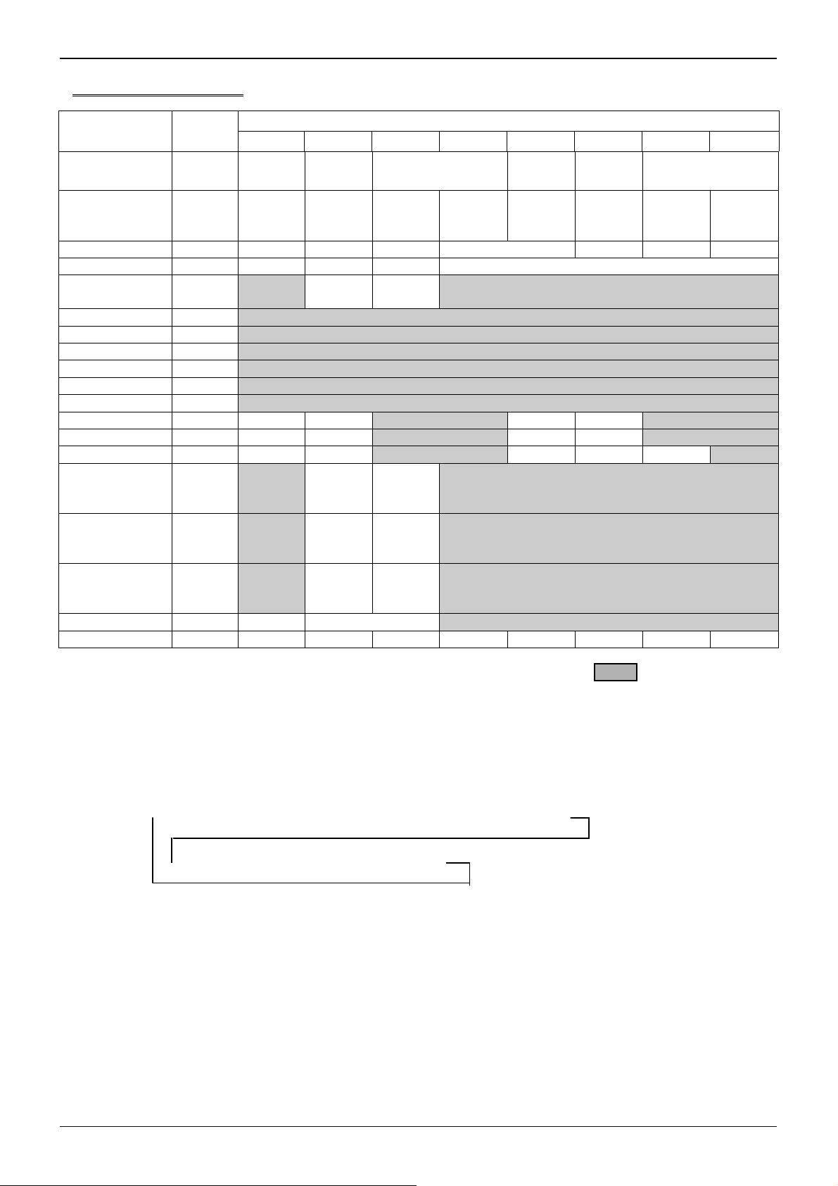
●Line up matrix
Function Specifications
Input selector
Input gain
Mute ・Possible to use “Advanced switch” for prevention of switching noise.
Volume
Bass
Middle
Treble
Fader
Loudness
LPF
Level meter
●Absolute maximum ratings (Ta=25℃)
・Stereo 4 input
・Differential 1 input
・0~20dB(1dB step)
・Possible to use “Advanced switch” for prevention of switching noise.
・+15dB~-79dB(1dB step), -∞
・Possible to use “Advanced switch” for prevention of switching noise.
・-20~+20dB(1dB step)
・Q=0.5, 1, 1.5, 2 variable
・fo=60, 80, 100, 120Hz
・Possible to use “Advanced switch” at changing gain
・-20~+20dB(1dB step)
・Q=0.75, 1, 1.25, 1.5 variable
・fo=500, 1k, 1.5k, 2.5kHz variable
・Possible to use “Advanced switch” at changing gain
・-20~+20dB(1dB step)
・Q=0.75, 1.25 variable
・fo=7.5k, 10k, 12.5k, 15kHz variable
・Possible to use “Advanced switch” at changing gain
・+15dB~-79dB(1dB step), -∞dB
・Possible to use “Advanced switch” for prevention of switching noise.
・0dB~20dB(1dB step)
・fo=250/400/800Hz
・Possible to use “Advanced switch” for prevention of switching noise.
・fc=55/85/120/160Hz, pass
・Phase shift (0°/180°)
・I2C BUS control
・DC Output
Technical Note
Item Symbol Rating Unit
Power supply Voltage VCC 10.0 V
Input voltage Vin
Power Dissipation Pd 1000 ※1 mW
Storage Temperature Ta stg -55~+150 ℃
※This value decreases 8mW/℃ for Ta=25℃ or more.
ROHM standard board shall be mounted.
Thermal resistance θja = 125(℃/W)
ROHM Standard board
Size:70×70×1.6(㎣)
Material:A FR4 grass epoxy board(3% or less of copper foil area)
●Operating conditions
Item Symbol MIN TYP MAX Unit
Power supply Voltage VCC 7.0 - 9.5 V
Temperature Topr -40 - +85
VCC+0.3~GND-0.3
V
℃
www.rohm.com
2/25
© 2010 ROHM Co., Ltd. All rights reserved.
2010.03 - Rev.A
Page 3
BD37524FS
Technical Note
●Electrical characteristics
(Unless specified particularly, Ta=25℃, VCC=8.5V, f=1kHz, Vin=1Vrms, Rg=600Ω, RL=10kΩ, A1 input, Input gain 0dB,
Mute off, Volume 0dB, Tone control 0dB, Loudness 0dB, LPF OFF, Fader 0dB)
Limit
BLOCK
Item Symbol
Min. Typ. Max.
Unit Condition
Current upon no signal IQ - 38 48 mA No signal
Voltage gain GV -1.5 0 1.5 dB Gv=20log(VOUT/VIN)
Channel balance CB -1.5 0 1.5 dB CB = GV1-GV2
T otal harmonic distortion 1
(FRONT,REAR)
T otal harmonic distortion 2
(SUBWOOFER)
Output noise voltage 1
(FRONT,REAR)*
Output noise voltage 2
(SUBWOOFER)*
GENERAL
THD+N1 - 0.001 0.05 %
THD+N2 - 0.002 0.05 %
V
V
Residual output noise voltage* V
- 3.8 15 μVrms
NO1
- 4.8 15 μVrms
NO2
- 1.8 10 μVrms
NOR
VOUT=1Vrms
BW=400-30KHz
VOUT=1Vrms
BW=400-30KHz
Rg = 0Ω
BW = IHF-A
Rg = 0Ω
BW = IHF-A
Fader = -∞dB
Rg = 0Ω
BW = IHF-A
Rg = 0Ω
Cross-talk between channels* CTC - -100 -90 dB
CTC=20log(VOUT/VIN)
BW = IHF-A
f=1kHz
Ripple rejection RR - -70 -40 dB
VRR=100mVrms
RR=20log(VCC IN/VOUT)
Input impedance(A, B) R
Input impedance (C,D,E) R
Maximum input voltage VIM 2.1 2.3 - Vrms
70 100 130 kΩ
IN_S
175 250 325 kΩ
IN_D
VIM at THD+N(VOUT)=1%
BW=400-30KHz
Rg = 0Ω
Cross-talk between selectors* CTS - -100 -90 dB
CTS=20log(VOUT/VIN)
BW = IHF-A
INPUT SELECTOR
Common mode rejection ratio* CMRR 50 65 - dB
CP1 and CN input
CP2 and CN input
CMRR=20log(VIN/VOUT)
BW = IHF-A
Input gain 0dB
Minimum input gain G
-2 0 +2 dB
IN MIN
VIN=100mVrms
Gin=20log(VOUT/VIN)
Input gain 20dB
Maximum input gain G
INPUT GAIN
Gain set error G
18 20 22 dB
IN MAX
VIN=100mVrms
Gin=20log(VOUT/VIN)
-2 0 +2 dB GAIN=+20~+1dB
IN ERR
Mute ON
Mute attenuation* G
MUTE
- -105 -85 dB
MUTE
Gmute=20log(VOUT/VIN)
BW = IHF-A
Volume = 15dB
Maximum gain G
13 15 17 dB
V MAX
VIN=100mVrms
Gv=20log(VOUT/VIN)
Volume = -∞dB
Maximum attenuation* G
VOLUME
Attenuation set error 1 G
Attenuation set error 2 G
Attenuation set error 3
- -100 -85 dB
V MIN
-2 0 2 dB GAIN & ATT=+15dB~-15dB
-3 0 3 dB ATT=-16dB~-47dB
-4 0 4 dB ATT=-48dB~-79dB
G
V ERR1
V ERR2
V ERR3
Gv=20log(VOUT/VIN)
BW = IHF-A
www.rohm.com
3/25
© 2010 ROHM Co., Ltd. All rights reserved.
2010.03 - Rev.A
Page 4
BD37524FS
BLOCK
Maximum boost gain
BASS
Maximum cut gain
Gain set error
Maximum boost gain
MIDDLE
Maximum cut gain
Gain set error
Maximum boost gain
TREBLE
Maximum cut gain
Gain set error
Maximum boost gain G
Maximum attenuation*
Gain set error
Attenuation set error 1
Attenuation set error 2
FADER / SUBWOOFER
Attenuation set error 3
Output impedance
Maximum output voltage
Maximum gain
LOUDNESS
Gain set error
Maximum output voltage V
Level
meter
Output offset voltage V
VP-9690A(Average value detection, effective value display) filter by Matsushita Communication is used for * measurement.
Phase between input / output is same.
Item Symbol
G
B BST
G
B CUT
G
B ERR
G
M BST
G
M CUT
G
M ERR
G
T BST
G
T CUT
G
T ERR
F BST
G
F MIN
G
F ERR
G
F ERR1
G
F ERR2
G
F ERR3
R
OUT
V
OM
G
L MAX
G
L ERR
L MAX
L OFF
Min. Typ. Max.
18 20 22 dB
-22 -20 -18 dB
18 20 22 dB
-22 -20 -18 dB
17 20 23 dB
-23 -20 -17 dB
-2 0 2 dB
13 15 17 dB
-
- - 50 Ω VIN=100mVrms
2 2.2
17 20 23 dB
-2 0 2 dB GAIN=+20~+1dB
2.8 3.1 3.5 V
-
Limit
Unit Condition
-2 0 2 dB Gain=-20~+20dB f=100Hz
-2 0 2 dB Gain=-20~+20dB f=1kHz
-100 -90 dB
-2 0 2 dB Gain=+1~+15dB
-2 0 2 dB ATT=-1~-15dB
-3 0 3 dB
-4 0 4 dB ATT=-48~-79dB
-
Vrms
0 100 mV
Technical Note
Gain=+20dB f=100Hz
VIN=100mVrms
GB=20log (VOUT/VIN)
Gain=-20dB f=100Hz
VIN=2Vrms
GB=20log (VOUT/VIN)
Gain=+20dB f=1kHz
VIN=100mVrms
GM=20log (VOUT/VIN)
Gain=-20dB f=1kHz
VIN=2Vrms
GM=20log (VOUT/VIN)
Gain=+20dB f=10kHz
VIN=100mVrms
GT=20log (VOUT/VIN)
Gain=-20dB f=10kHz
VIN=2Vrms
G
=20log (VOUT/VIN)
T
Gain=-20~+20dB f=10kHz
Fader=15dB
V
=100mVrms
IN
G
=20log(VOUT/VIN)
F
Fader = -∞dB
G
=20log(VOUT/VIN)
F
BW = IHF-A
ATT=-16~-47dB
THD+N=1%
BW=400-30KHz
Gain 20dB
VIN=100mVrms
G
=20log(VOUT/VIN)
L
www.rohm.com
4/25
© 2010 ROHM Co., Ltd. All rights reserved.
2010.03 - Rev.A
Page 5
BD37524FS
%
u
dB
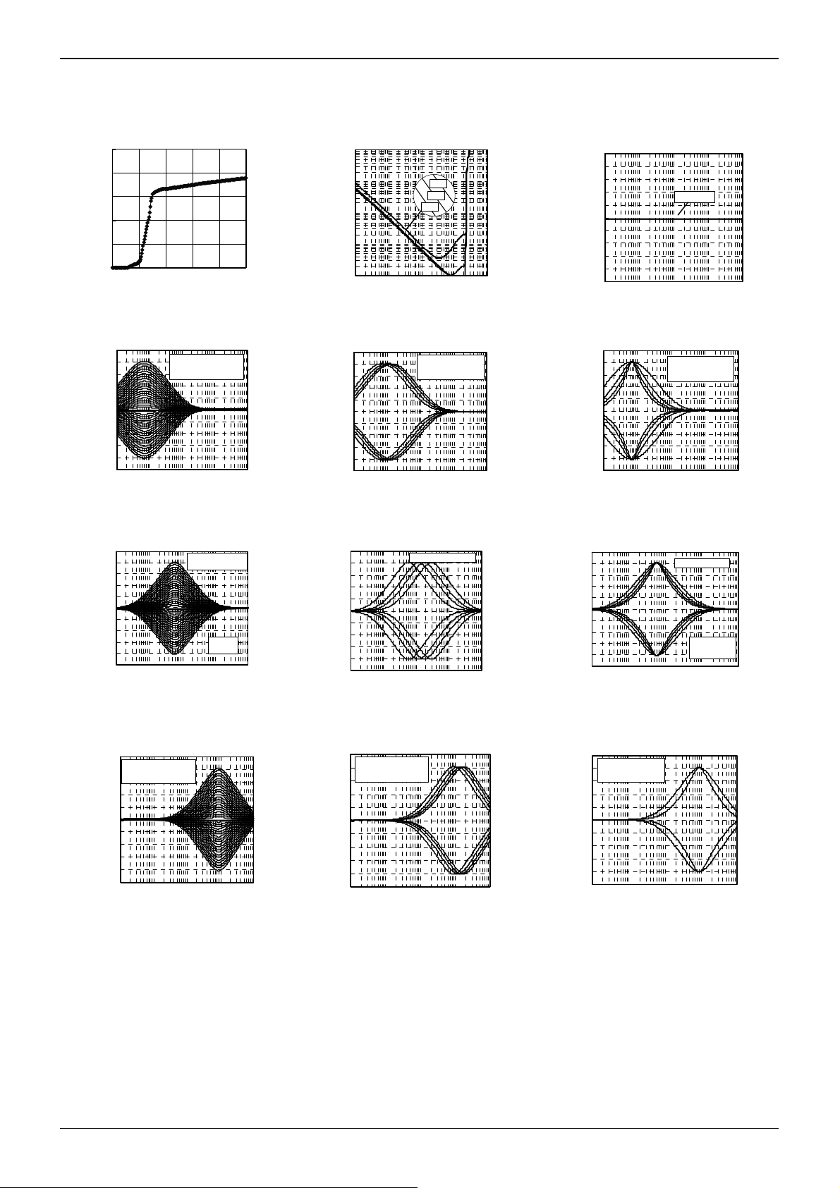
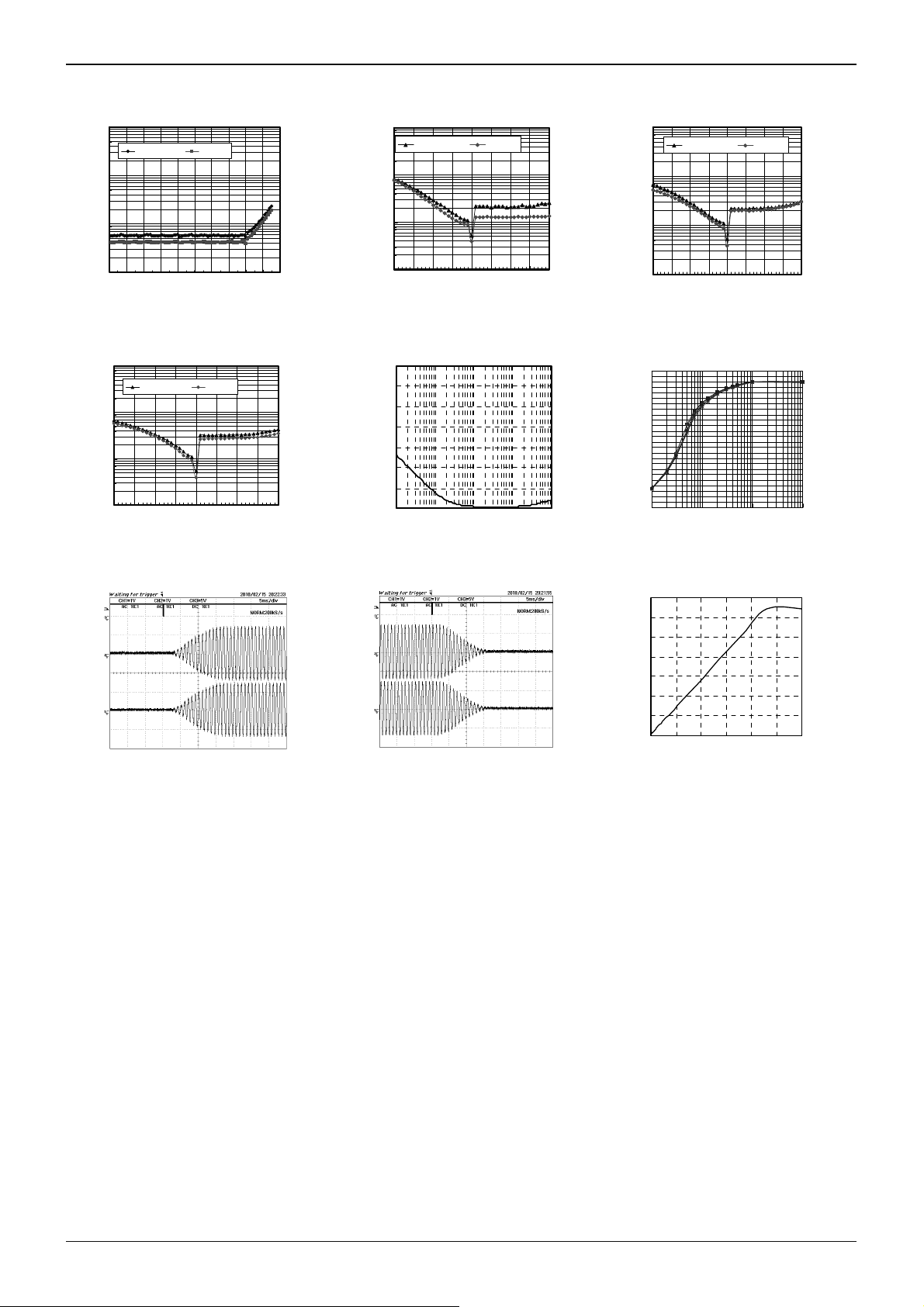
●Electrical characteristic curves (Reference data)
Technical Note
50
40
30
Iq[mA]
20
10
0
0246810
VCC[V]
Fig.1 Iq vs Vcc
25
20
15
10
5
Gain[dB]
0
-5
-1 0
-1 5
-2 0
-2 5
10 100 1k 10k 100k
BASS GAIN : -20~+20dB
/1dB step
fo : 60Hz Q : 0.5
Frequency [Hz]
Fig.4 Bass Gain vs Freq
25
20
15
10
5
0
-5
Gain[dB]
-1 0
-1 5
-2 0
-2 5
10 100 1k 10k 100k
MIDDLE GAIN :
-20~+20dB /1dB step
Frequency [Hz]
fo : 500Hz
Q : 0.75
Fig.7 Middle Gain vs Freq
10
1
0.1
THD+N (
THD+N[%]
0.01
0.001
0.0 0 1 0 .0 1 0.1 1 10
25
20
15
10
5
Gain[dB]
0
-5
-1 0
-1 5
-2 0
-2 5
10 100 1k 10k 100k
Vout [Vrms]
Fig.2 Thd vs Vo
Frequency [Hz]
Fig.5 Bass fo vs Freq
25
20
15
10
5
0
-5
Gain[dB]
-1 0
-1 5
-2 0
-2 5
10 100 1k 10k 100k
Frequency [Hz]
Fig.8 Middle fo vs Freq Fig.9 Middle Q vs Freq
10kHz
1kHz
100Hz
Vout (V)
fo : 60/80/100/120Hz
BASS GAIN : ±20dB
Q : 0.5
fo : 500/1k/1.5k/2.5kHz
10
1
0.1
0.01
0.001
5
4
3
Vo
Vin[Vrms]
2
1
0
Gain[dB]
Gain (
-1
10 100 1k 10k 100k
-2
-3
-4
-5
Fig.3 Gain vs Freq
Fig.12 Gain vs Freq
25
20
15
10
5
0
Gain[dB]
-5
-1 0
-1 5
-2 0
-2 5
10 100 1k 10k 100k
Gain=0dB
Frequency [Hz]
Frequency (Hz)
Q : 0.5/1/1.5/2
BASS GAIN : ±20dB
fo : 60Hz
Frequency [Hz]
Fig.6 Bass Q vs Freq
25
20
15
10
5
0
-5
Gain[dB]
-10
-15
-20
-25
10 100 1k 10k 100k
Q : 0.75/1/1.25/1.5
Frequency [Hz]
MIDDLE GAIN :
±20dB
fo : 1kHz
25
TREBLE GAIN:-20~+20dB
20
/1dB step
fo : 7.5kHz Q : 0. 75
15
10
5
0
-5
Gain (dB)
Gain[dB]
-10
-15
-20
-25
10 100 1k 10k 100k
Frequency [Hz]
Frequency (Hz)
25
fo : 7.5k/10k/12.5k/15kHz
TREBLE GAIN : ±20dB
20
Q : 0.75
15
10
5
0
Output
-5
Noise[uVrm
-10
-15
-20
-25
10 100 1k 10k 100k
Frequency [Hz]
Fig.10 Treble Gain vs Freq Fig.11 Treble fo vs Freq Fig.12 Treble Q vs Freq
www.rohm.com
5/25
© 2010 ROHM Co., Ltd. All rights reserved.
25
Q : 0.75/1.25
20
TREBLE GAIN : ±20dB
fo : 7.5kHz
15
10
5
0
-5
Gain (dB)
Gain[dB]
-10
-15
-20
-25
10 100 1k 10k 100k
Frequency [Hz]
Frequency (Hz)
2010.03 - Rev.A
Page 6
BD37524FS
B
g
1000
100
Din-Audio IHF-A
1000
100
DIN-Audio IHF-A
Technical Note
1000
DIN-Audio IHF-A
100
10
Output Noise[uVrms]
出力雑音電圧[uVrms]
1
-80 -70 -60 -50 -40 -30 -20 -10 0 10 20
Volume Gain[dB]
Fig.13 Volume Gain vs Noise
1000
DIN-Audio IHF-A
100
10
Output Noise[uVrms]
出力雑音電圧 [uVrms]
1
-20 -15 -10 -5 0 5 10 15 20
Treble Gain [dB]
Fig.16 Treble Gain vs Noise
10
Output Noise[uVrms]
出力雑音電圧 [uVrms]
1
-20 -15 -10 -5 0 5 10 15 20
0
-1 0
-2 0
-3 0
Gain[dB]
-4 0
Gain (d
-5 0
-6 0
-7 0
10 100 1k 10k 100k
Bass Gain [dB]
.14 Bass Gain vs Noise
Fi
Frequency [Hz]
Frequency (Hz)
Fig.17 CMRR vs Freq
10
出力雑音電圧 [uVrms]
1
-20 -15 -10 -5 0 5 10 15 20
Middle Gain [dB]
Fig.15 Middle Gain vs Noise
2.5
2.0
1.5
1.0
Vo [Vrms]
最大出力[Vrms]
0.5
0.0
100 1000 10000 100000
Rload [ohm]
出力負荷[ohm]
Fig.18 Rload vs Vo
3.5
3
2.5
2
1.5
Vout[V]
1
0.5
0
00.511.522.53
Vin [Vrms]
Fig.19 Advanced Switch 1
Fig.20 Advanced Switch 2 Fig.21 Level Meter Vin vs Vo
www.rohm.com
6/25
© 2010 ROHM Co., Ltd. All rights reserved.
2010.03 - Rev.A
Page 7
BD37524FS
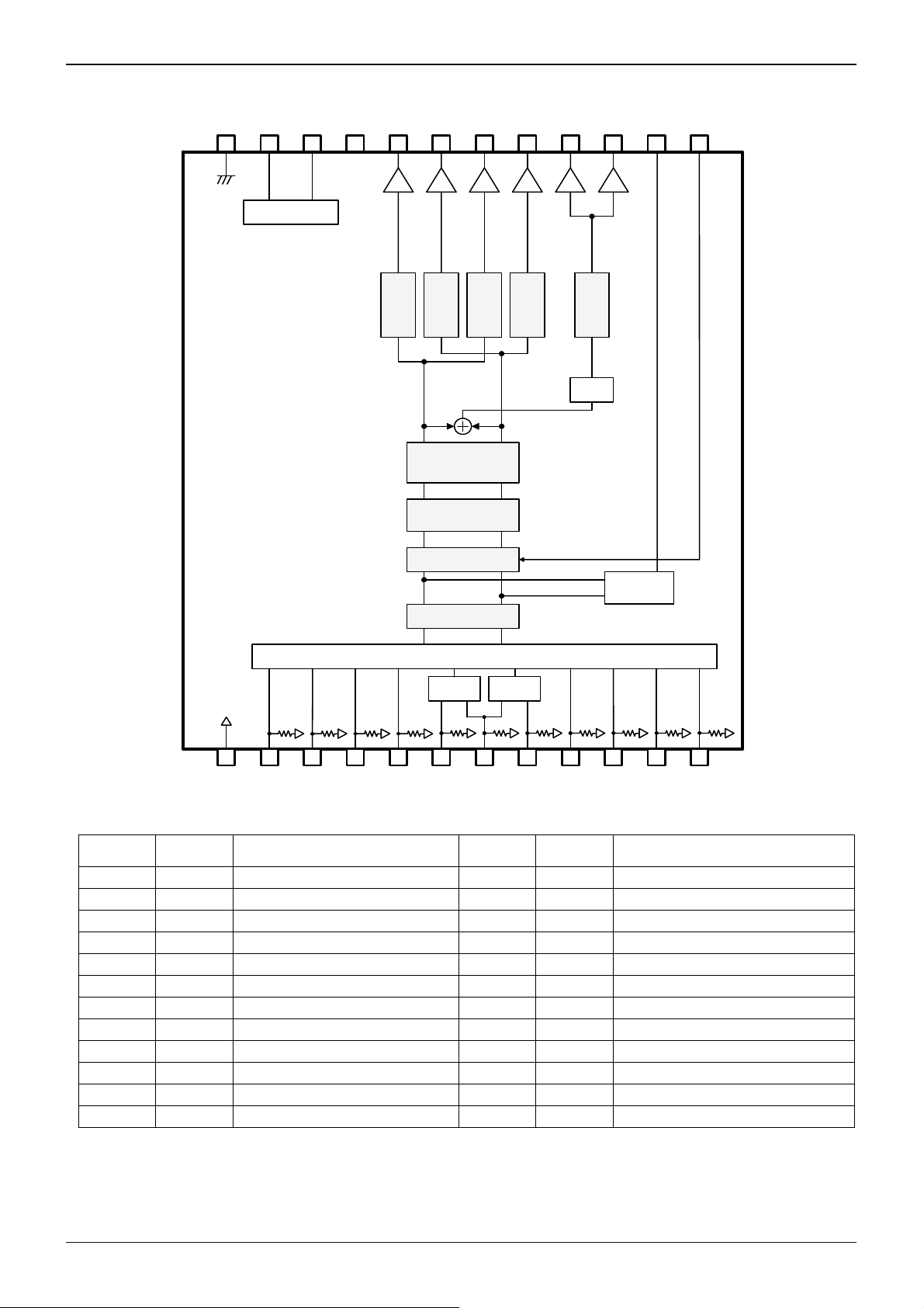
●Block diagram and pin configuration
GND
I2C BUS LOGIC
VCC
■Fader
Gain:+15dB~-79dB/1dB step
★no pop noise
■LPF
fc=55/85/120/160Hz
■Loudness
Gain:20dB~0dB/1dB step
★no pop noise
・f0=250/400/800Hz
・Hicut:1/2/3/4
■3 Band P-EQ (Tone control)
Gain:+20dB~-20dB/1dB step
★no pop noise
・Bass:f0=60/80/100/120Hz
Q=0.5/1.0/1.5/2.0
・Meddle:f0=500/1k/1.5k/2.5kHz
Q=0.75/1/1.25/1.5
・Treble:f0=7.5k/10k/12.5k/15kHz
Q=0.75/1.25
■Volume
Gain:+15dB~-79dB/1dB step
★no pop noise
■Input Gain
Gain:+20dB~0dB/1dB step
★no pop noise
Fader★
Fader★
★Loudness
★3 Band P-EQ
(Tone control)
★Volume/Mute
★Input Gain
Input selector (4 single-end and 1 stereo ISO)
VCC/2
100k 100k 100k 100k 250k
1 2 3 4 5 6 7 8
ISO amp
Fig.22 BD37524FS
Descriptions of terminal
Terminal
No.
Terminal
Name
Description
1 FIL VCC/2 terminal 13 MUTE External compulsory mute terminal
2 A1 A input terminal of 1ch 14 LOUT Output terminal for Level meter
3 A2 A input terminal of 2ch 15 OUTS2 Subwoofer output terminal of 2ch
4 B1 B input terminal of 1ch 16 OUTS1 Subwoofer output terminal of 1ch
5 B2 B input terminal of 2ch 17 OUTR2 Rear output terminal of 2ch
6 CP1 C positive input terminal of 1ch 18 OUTR1 Rear output terminal of 1ch
7 CN C negative input terminal 19 OUTF2 Front output terminal of 2ch
8 CP2 C positive input terminal of 2ch 20 OUTF1 Front output terminal of 1ch
9 D1 D input terminal of 1ch 21 VCC Power supply terminal
10 D2
11 E1
12 E2
D input terminal of 2ch
E input terminal of 1ch
E input terminal of 2ch
GND
Technical Note
14
1324 23 22 21 20 19 18 17 16 15
Fader★
Fader★
GND
ISO amp
250k250k 250k 250k 250k 250k
Terminal
No.
22 SCL I2C Communication clock terminal
23 SDA I2C Communication data terminal
24 GND GND terminal
Fader★
LPF
9
Terminal
Name
Level
meter
10 11 12
Description
www.rohm.com
7/25
© 2010 ROHM Co., Ltd. All rights reserved.
2010.03 - Rev.A
Page 8
BD37524FS
Technical Note
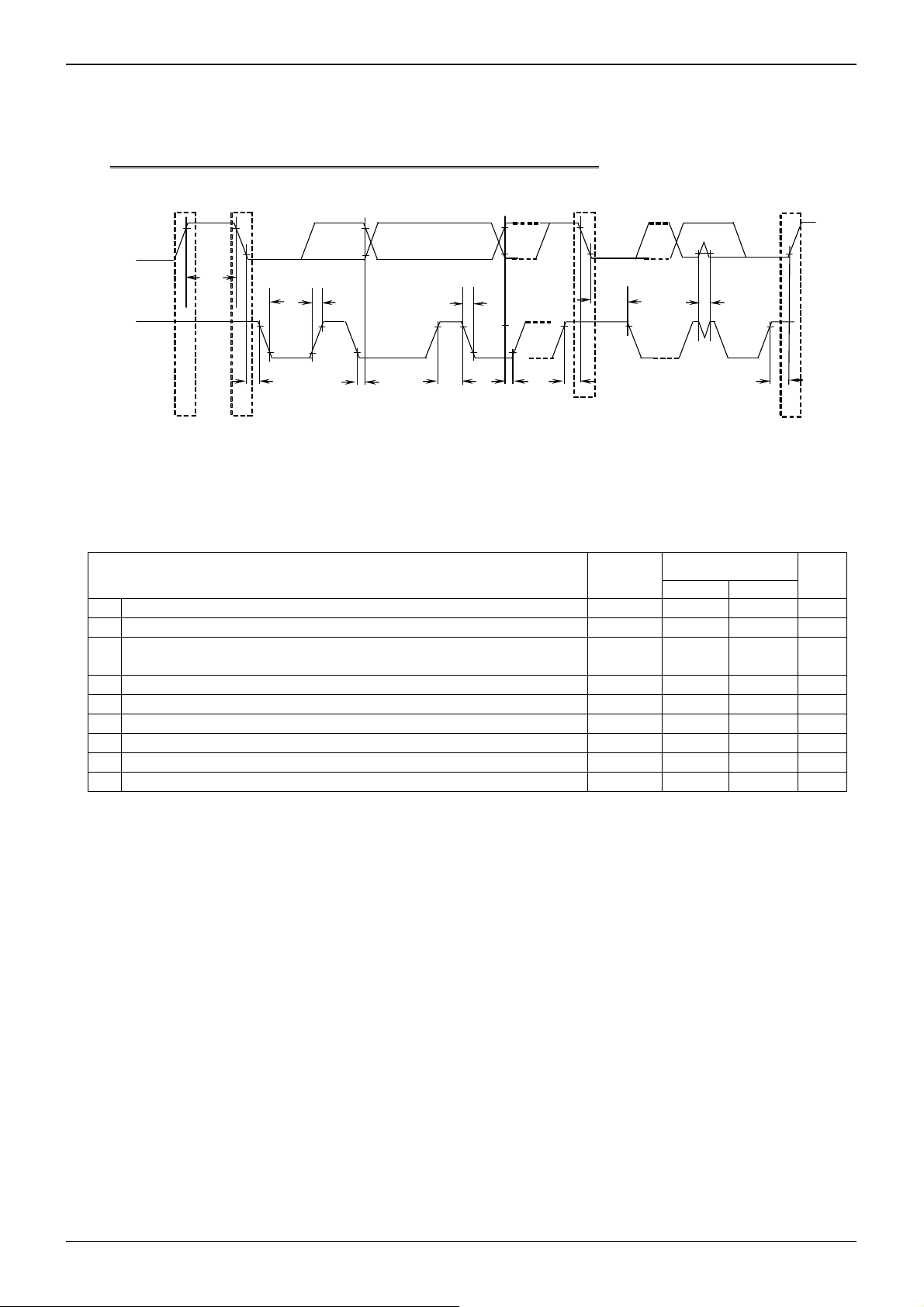
●Timming Chart
CONTROL SIGNAL SPECIFICATION
(1) Electrical specifications and timing for bus lines and I/O stages
SDA
SCL
t
BUF
t
LOW
t
t
R
F
t
HD;STA
t
SP
P
t
HD;STA
S
t
HD;DAT
t
HIGH
t
SU;D AT tSU;STA
Sr
t
SU;STO
2
Fig.23 Definition of timing on the I
Table 1 Characteristics of the SDA and SCL bus lines for I
2
C-bus devices
C-bus
(Unless specified particularly, Ta=25℃, VCC=8.5V)
Parameter Symbol
Fast-mode I2C-bus
Min. Max.
1 SCL clock frequency fSCL 0
400 kHz
2 Bus free time between a STOP and START condition tBUF 1.3 - μS
Hold time (repeated) START condition. After this period, the first
3
clock pulse is generated
tHD;STA 0.6 - μS
4 LOW period of the SCL clock tLOW 1.3 - μS
5 HIGH period of the SCL clock tHIGH 0.6 - μS
6 Set-up time for a repeated START condition tSU;STA 0.6 - μS
7 Data hold time: tHD;DAT 0.06* - μS
8 Data set-up time tSU;DAT 120 - ns
9 Set-up time for STOP condition tSU;STO 0.6 - μS
All values referred to VIH min. and VIL max. Levels (see Table 2).
* A device must internally provide a hold time of at least 300 ns for the SDA signal (referred to the VIH min. of the SCL
signal) in order to bridge the undefined region of the falling edge of SCL.
About 7(tHD;DAT), 8(tSU;DAT), make it the setup which a margin is fully in .
P
Unit
www.rohm.com
8/25
© 2010 ROHM Co., Ltd. All rights reserved.
2010.03 - Rev.A
Page 9
BD37524FS
Technical Note
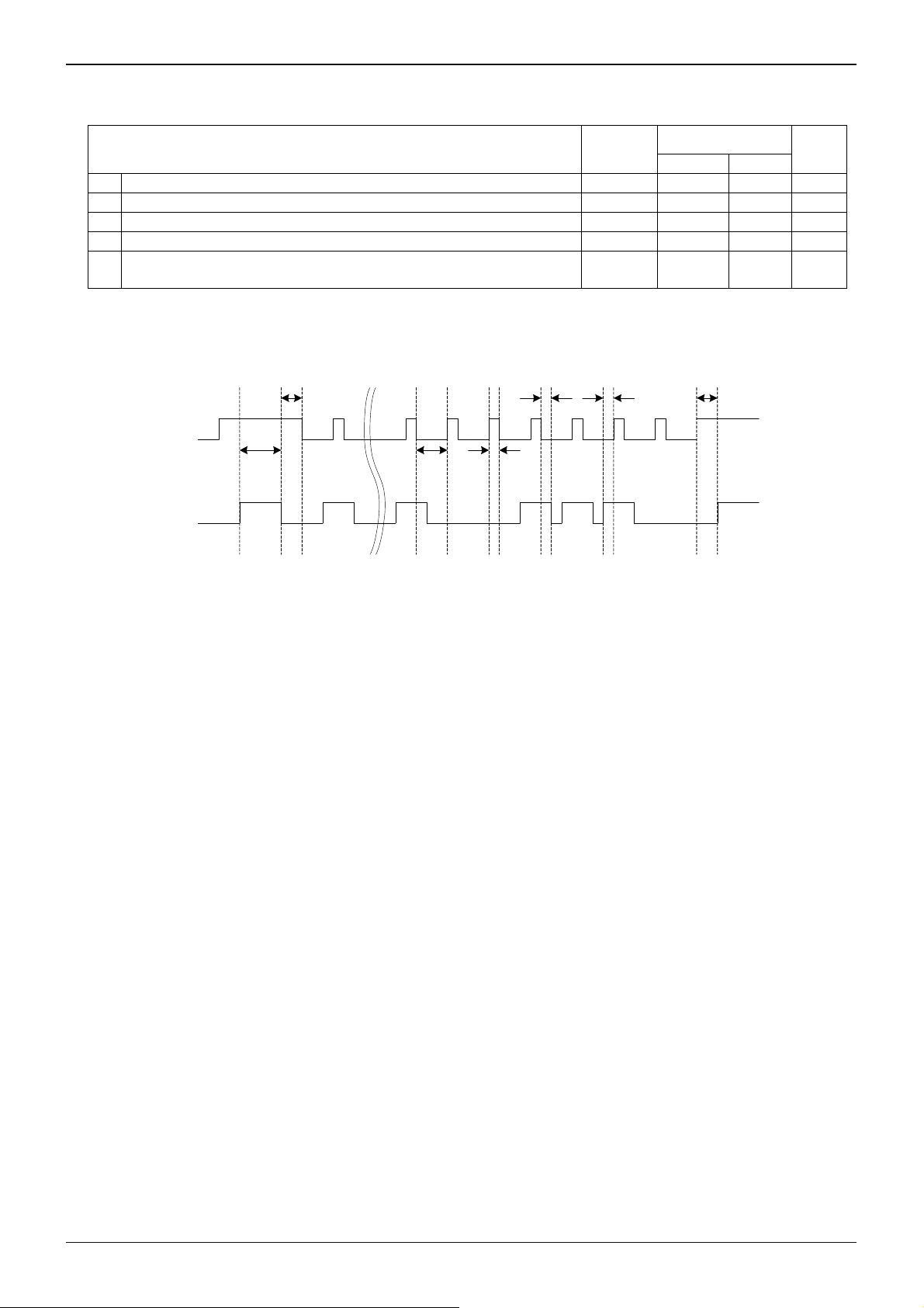
Table 2 Characteristics of the SDA and SCL I/O stages for I
Parameter Symbol
10
LOW level input voltage:
11
HIGH level input voltage:
Pulse width of spikes which must be suppressed by the input filter.
12
13
LOW level output voltage: at 3mA sink current
Input current each I/O pin with an input voltage between 0.4V and
14
4.5V.
tHD;STA
:2us
SCL
tBUF
:4us
tLOW
:3us
SDA
2
C-bus devices
tHD;DAT
:1us
tHIGH
:1us
Fast-mode devices
Min. Max.
VIL -0.3 1 V
VIH 2.3 5 V
tSP 0 50 ns
VOL1 0 0.4 V
Ii -10 10 μA
tSU;DAT
:1us
tSU;STO
:2us
Unit
SCL clock frequency:250kHz
Fig.24 A command timing example in the I2C data transmission
www.rohm.com
9/25
© 2010 ROHM Co., Ltd. All rights reserved.
2010.03 - Rev.A
Page 10

BD37524FS
(2)I2C BUS FORMAT
MSB LSB MSB LSB MSB LSB
S Slave Address A Select Address A Data A P
1bit 8bit 1bit 8bit 1bit 8bit 1bit 1bit
S = Start conditions (Recognition of start bit)
Slave Address = Recognition of slave address. 7 bits in upper order are voluntary.
The least significant bit is “L” due to writing.
A = ACKNOWLEDGE bit (Recognition of acknowledgement)
Select Address = Select every of volume, bass and treble.
Data = Data on every volume and tone.
P = Stop condition (Recognition of stop bit)
(3)I
(4)Slave address
2
C BUS Interface Protocol
1)Basic form
S Slave Address A Select Address A Data A P
MSB LSB MSB LSB MSB LSB
2)Automatic increment (Select Address increases (+1) according to the number of data.
S Slave Address A Select Address A Data1 A Data2 A ・・・・ DataN A P
MSB LSB MSB LSB MSB LSB MSB LSB MSB LSB
(Example) ①Data1 shall be set as data of address specified by Select Address.
②Data2 shall be set as data of address specified by Select Address +1.
③DataN shall be set as data of address specified by Select Address +N-1.
3)Configuration unavailable for transmission (In this case, only Select Address1 is set.
S Slave Address A Select Address1 A Data A Select Address 2 A Data A P
MSB LSB MSB LSB MSB LSB MSB LSB MSB LSB
(Note)If any data is transmitted as Select Address 2 next to data, it is
recognized as data, not as Select Address 2.
MSB LSB
A6 A5 A4 A3 A2 A1 A0 R/W
1 0 0 0 0 0 0 0
80H
Technical Note
www.rohm.com
10/25
© 2010 ROHM Co., Ltd. All rights reserved.
2010.03 - Rev.A
Page 11
BD37524FS
(5)Select Address & Data
Items
Initial setup 1 01
Initial setup 2 02
Initial setup 3 03 0 0 0 Loudness fo 0 0 1
Input Selector 05 0 0 0 Input selector
Input gain 06
Volume gain 20 Volume Gain / Attenuation
Fader 1ch Front 28 Fader Gain / Attenuation
Fader 2ch Front 29 Fader Gain / Attenuation
Fader 1ch Rear 2A Fader Gain / Attenuation
Fader 2ch Rear 2B Fader Gain / Attenuation
Fader Subwoofer 2C Fader Gain / Attenuation
Bass setup 41 0 0 Bass fo 0 0 Bass Q
Middle setup 44 0 0 Middle fo 0 0 Middle Q
Treble setup 47 0 0 Treble fo 0 0 0 Treble Q
Bass gain 51
Middle gain 54
Treble gain 57
Loudness Gain 75 0 Loudness Hicut Loudness Gain
System Reset FE 1 0 0 0 0 0 0 1
Note
1.In function changing of the hatching part, it works Advanced switch.
2.Upon continuous data transfer, the Select Address is circulated by the automatic increment function, as
shown below.
3.For the function of input selector etc, it is not corresponded for advanced switch. Therefore, please apply mute on
the side of a set when changes these setting.
4.When using mute function of this IC at the time of changing input selector, please switch mute ON/OFF for waiting
advanced-mute time.
Select
Address
(hex)
→01→02→03→05→06→20→28→29→2A→2B→2C
→41→44→47→51→54→57→75
MSB Data LSB
D7 D6 D5 D4 D3 D2 D1 D0
Advanced
switch
ON/OFF
LPF
Phase
Mute
ON/OFF
Bass
Boost/
Cut
Middle
Boost/
Cut
Treble
Boost/
Cut
0
Level
Meter
RESET
0 0
0 0 Bass Gain
0 0 Middle Gain
0 0 Treble Gain
Advanced switch time
of Input Gain/Volume
Tone/Fader/Loudness
0 0 0
0 0
Subwoofer
LPF fc
Input Gain
Technical Note
Advanced switch time
of Mute
LPF
Phase
Advanced switch
Level
Meter
RESET
www.rohm.com
11/25
© 2010 ROHM Co., Ltd. All rights reserved.
2010.03 - Rev.A
Page 12

BD37524FS
Select address 01 (hex)
Time
0.6msec
1.0msec 0 1
1.4msec 1 0
3.2msec 1 1
Time
4.7 msec
7.1 msec 0 1
11.2 msec 1 0
14.4 msec 1 1
Mode
OFF 0
ON 1
Select address 02(hex)
fc
OFF
55Hz 0 0 1
85Hz 0 1 0
120Hz 0 1 1
160Hz 1 0 0
Prohibition Other setting
Mode
HOLD
RESET 1
Phase
0° 0
180° 1
Select address 03(hex)
f0
250Hz
400Hz 0 1
800Hz 1 0
Prohibition 1 1
Technical Note
MSB Advanced switch time of Mute LSB
D7 D6 D5 D4 D3 D2 D1 D0
Advanced
Switch
ON/OFF
MSB
D7 D6 D5 D4 D3 D2 D1 D0
Advanced
Switch
ON/OFF
MSB Advanced switch ON/OFF LSB
D7 D6 D5 D4 D3 D2 D1 D0
MSB Subwoofer LPF fc LSB
D7 D6 D5 D4 D3 D2 D1 D0
LPF Phase
MSB Level Meter RESET LSB
D7 D6 D5 D4 D3 D2 D1 D0
LPF Phase
MSB LPF Phase LSB
D7 D6 D5 D4 D3 D2 D1 D0
MSB Loudness fo LSB
D7 D6 D5 D4 D3 D2 D1 D0
0 0 0
0
Input gain/Volume/Tone/Fader/Loudness
0
0
Level
Meter
RESET
0
Level
Meter
RESET
Advanced switch time
of Input gain/Volume
Tone/Fader/Loudness
Advanced switch time of
0 0
Advanced switch time
of Input gain/Volume
Tone/Fader/Loudness
0 0 0
0 0 0 Subwoofer LPF fc
0 0 0 Subwoofer LPF fc
0 0
0 0
0 0
0 0
0 0 0
0 0 1
: Initial condition
0 0
Advanced switch Time
of Mute
Advanced switch
Time of Mute
LSB
www.rohm.com
12/25
© 2010 ROHM Co., Ltd. All rights reserved.
2010.03 - Rev.A
Page 13

BD37524FS
Select address 05(hex)
Mode
A A1 A2
B B1 B2 0 0 1 0
C diff CP1 CP2 0 1 1 0
D D1 D2 1 0 1 0
E E1 E2 1 0 1 1
Input SHORT:The input impedance of each input terminal is lowered from 100kΩ(TYP) to 6 kΩ(TYP).
Select address 06 (hex)
OUT
F1/R1
Input SHORT 1 0 0 1
Prohibition Other setting
Gain
0dB
1dB 0 0 0 0 1
2dB 0 0 0 1 0
3dB 0 0 0 1 1
4dB 0 0 1 0 0
5dB 0 0 1 0 1
6dB 0 0 1 1 0
7dB 0 0 1 1 1
8dB 0 1 0 0 0
9dB 0 1 0 0 1
10dB 0 1 0 1 0
11dB 0 1 0 1 1
12dB 0 1 1 0 0
13dB 0 1 1 0 1
14dB 0 1 1 1 0
15dB 0 1 1 1 1
16dB 1 0 0 0 0
17dB 1 0 0 0 1
18dB 1 0 0 1 0
19dB 1 0 0 1 1
20dB 1 0 1 0 0
Prohibition
Mode
OFF 0
ON 1
OUT
F2/R2
(For quick charge of coupling capacitor)
MSB Input Selector LSB
D7 D6 D5 D4 D3 D2 D1 D0
0 0 0 1
0 0 0 0
MSB Input Gain LSB
D7 D6 D5 D4 D3 D2 D1 D0
0 0 0 0 0
Mute
ON/OFF
MSB Mute ON/OFF LSB
D7 D6 D5 D4 D3 D2 D1 D0
0 0
1 1 0 1 1
:
1 1 1 1 1
0 0 Input Gain
:
: : :
Technical Note
: Initial condition
www.rohm.com
13/25
© 2010 ROHM Co., Ltd. All rights reserved.
2010.03 - Rev.A
Page 14
BD37524FS
Select address 20, 28, 29, 2A, 2B, 2C (hex)
Gain & ATT
Prohibition
15dB 0 1 1 1 0 0 0 1
14dB 0 1 1 1 0 0 1 0
13dB 0 1 1 1 0 0 1 1
-77dB 1 1 0 0 1 1 0 1
-78dB 1 1 0 0 1 1 1 0
-79dB 1 1 0 0 1 1 1 1
Prohibition
-∞dB 1 1 1 1 1 1 1 1
:
MSB Vol, Fader Gain / Attenuation LSB
D7 D6 D5 D4 D3 D2 D1 D0
0 0 0 0 0 0 0 0
0 0 0 0 0 0 0 1
: : : : : : : :
0 1 1 1 0 0 0 0
: : : : : : : :
1 1 0 1 0 0 0 0
: : : : : : : :
1 1 1 1 1 1 1 0
Technical Note
: Initial condition
www.rohm.com
14/25
© 2010 ROHM Co., Ltd. All rights reserved.
2010.03 - Rev.A
Page 15

BD37524FS
Select address 41(hex)
Q factor
0.5
1.0 0 1
1.5 1 0
2.0 1 1
fo
60Hz
80Hz 0 1
100Hz 1 0
120Hz 1 1
Select address 44(hex)
Q factor
0.75
1.0 0 1
1.25 1 0
1.5 1 1
fo
500Hz
1kHz 0 1
1.5kHz 1 0
2.5kHz 1 1
Select address 47 (hex)
Q factor
0.75
1.25 1
fo
7.5kHz
10kHz 0 1
12.5kHz 1 0
15kHz 1 1
Technical Note
MSB Bass Q factor LSB
D7 D6 D5 D4 D3 D2 D1 D0
0 0
0 0 Bass fo 0 0
MSB Bass fo LSB
D7 D6 D5 D4 D3 D2 D1 D0
0 0
0 0
MSB Middle Q factor LSB
D7 D6 D5 D4 D3 D2 D1 D0
0 0 Middle fo 0 0
MSB Middle fo LSB
D7 D6 D5 D4 D3 D2 D1 D0
0 0
0 0
MSB Treble Q factor LSB
D7 D6 D5 D4 D3 D2 D1 D0
0 0 Treble fo 0 0 0
MSB Treble fo LSB
D7 D6 D5 D4 D3 D2 D1 D0
0 0
0 0
0 0
0 0
0 0 0
: Initial condition
Bass
Q factor
0 0
Middle
Q factor
Treble
Q factor
0
www.rohm.com
15/25
© 2010 ROHM Co., Ltd. All rights reserved.
2010.03 - Rev.A
Page 16

BD37524FS
Select address 51, 54, 57 (hex)
Gain
0dB
1dB 0 0 0 0 1
2dB 0 0 0 1 0
3dB 0 0 0 1 1
4dB 0 0 1 0 0
5dB 0 0 1 0 1
6dB 0 0 1 1 0
7dB 0 0 1 1 1
8dB 0 1 0 0 0
9dB 0 1 0 0 1
10dB 0 1 0 1 0
11dB 0 1 0 1 1
12dB 0 1 1 0 0
13dB 0 1 1 0 1
14dB 0 1 1 1 0
15dB 0 1 1 1 1
16dB 1 0 0 0 0
17dB 1 0 0 0 1
18dB 1 0 0 1 0
19dB 1 0 0 1 1
20dB 1 0 1 0 0
Prohibition
Mode
Boost 0
Cut 1
Technical Note
MSB Bass/ Middle/ Treble Gain LSB
D7 D6 D5 D4 D3 D2 D1 D0
0 0 0 0 0
Bass/
Middle/
Treble
Boost
/cut
MSB Bass/ Middle/ Treble Boost/Cut LSB
D7 D6 D5 D4 D3 D2 D1 D0
0 0
1 0 1 0 1
: : : : :
1 1 1 1 0
1 1 1 1 1
0 0 Bass/Middle/Treble Gain
: Initial condition
www.rohm.com
16/25
© 2010 ROHM Co., Ltd. All rights reserved.
2010.03 - Rev.A
Page 17

BD37524FS
Select address 75 (hex)
Mode
Hicut1
Hicut2 0 1
Hicut3 1 0
Hicut4 1 1
Gain
0dB
1dB 0 0 0 0 1
2dB 0 0 0 1 0
3dB 0 0 0 1 1
4dB 0 0 1 0 0
5dB 0 0 1 0 1
6dB 0 0 1 1 0
7dB 0 0 1 1 1
8dB 0 1 0 0 0
9dB 0 1 0 0 1
10dB 0 1 0 1 0
11dB 0 1 0 1 1
12dB 0 1 1 0 0
13dB 0 1 1 0 1
14dB 0 1 1 1 0
15dB 0 1 1 1 1
16dB 1 0 0 0 0
17dB 1 0 0 0 1
18dB 1 0 0 1 0
19dB 1 0 0 1 1
20dB 1 0 1 0 0
Prohibition
(6)About power on reset
At on of supply voltage circuit made initialization inside IC is built-in. Please send data to all address
as initial data at supply voltage on. And please supply mute at set side until this initial data is sent.
Item Symbol
Rise time of VCC Trise 33 - - usec VCC rise time from 0V to 5V
VCC voltage of release
power on reset
(7)About external compulsory mute terminal
Mute is possible forcibly than the outside after input again department, by the setting of the MUTE terminal.
MSB Loudness Hicut LSB
D7 D6 D5 D4 D3 D2 D1 D0
0 0
0
MSB Loudness Gain LSB
D7 D6 D5 D4 D3 D2 D1 D0
0 0 0 0 0
0 Loudness Hicut
1 0 1 0 1
: : : : :
1 1 1 1 1
Limit
Min. Typ. Max.
Vpor - 4.1 - V
Mute Voltage Condition Mode
GND~1.0V MUTE ON
2.3V~VCC MUTE OFF
Establish the voltage of MUTE in the condition to have been defined.
Loudness Gain
Unit Condition
Technical Note
: Initial condition
www.rohm.com
17/25
© 2010 ROHM Co., Ltd. All rights reserved.
2010.03 - Rev.A
Page 18

BD37524FS
Volume / Fader volume attenuation of the details
(dB)
+15 0 1 1 1 0 0 0 1 -33 1 0 1 0 0 0 0 1
+14 0 1 1 1 0 0 1 0 -34 1 0 1 0 0 0 1 0
+13 0 1 1 1 0 0 1 1 -35 1 0 1 0 0 0 1 1
+12 0 1 1 1 0 1 0 0 -36 1 0 1 0 0 1 0 0
+11 0 1 1 1 0 1 0 1 -37 1 0 1 0 0 1 0 1
+10 0 1 1 1 0 1 1 0 -38 1 0 1 0 0 1 1 0
+9 0 1 1 1 0 1 1 1 -39 1 0 1 0 0 1 1 1
+8 0 1 1 1 1 0 0 0 -40 1 0 1 0 1 0 0 0
+7 0 1 1 1 1 0 0 1 -41 1 0 1 0 1 0 0 1
+6 0 1 1 1 1 0 1 0 -42 1 0 1 0 1 0 1 0
+5 0 1 1 1 1 0 1 1 -43 1 0 1 0 1 0 1 1
+4 0 1 1 1 1 1 0 0 -44 1 0 1 0 1 1 0 0
+3 0 1 1 1 1 1 0 1 -45 1 0 1 0 1 1 0 1
+2 0 1 1 1 1 1 1 0 -46 1 0 1 0 1 1 1 0
+1 0 1 1 1 1 1 1 1 -47 1 0 1 0 1 1 1 1
0 1 0 0 0 0 0 0 0 -48 1 0 1 1 0 0 0 0
-1 1 0 0 0 0 0 0 1 -49 1 0 1 1 0 0 0 1
-2 1 0 0 0 0 0 1 0 -50 1 0 1 1 0 0 1 0
-3 1 0 0 0 0 0 1 1 -51 1 0 1 1 0 0 1 1
-4 1 0 0 0 0 1 0 0 -52 1 0 1 1 0 1 0 0
-5 1 0 0 0 0 1 0 1 -53 1 0 1 1 0 1 0 1
-6 1 0 0 0 0 1 1 0 -54 1 0 1 1 0 1 1 0
-7 1 0 0 0 0 1 1 1 -55 1 0 1 1 0 1 1 1
-8 1 0 0 0 1 0 0 0 -56 1 0 1 1 1 0 0 0
-9 1 0 0 0 1 0 0 1 -57 1 0 1 1 1 0 0 1
-10 1 0 0 0 1 0 1 0 -58 1 0 1 1 1 0 1 0
-11 1 0 0 0 1 0 1 1 -59 1 0 1 1 1 0 1 1
-12 1 0 0 0 1 1 0 0 -60 1 0 1 1 1 1 0 0
-13 1 0 0 0 1 1 0 1 -61 1 0 1 1 1 1 0 1
-14 1 0 0 0 1 1 1 0 -62 1 0 1 1 1 1 1 0
-15 1 0 0 0 1 1 1 1 -63 1 0 1 1 1 1 1 1
-16 1 0 0 1 0 0 0 0 -64 1 1 0 0 0 0 0 0
-17 1 0 0 1 0 0 0 1 -65 1 1 0 0 0 0 0 1
-18 1 0 0 1 0 0 1 0 -66 1 1 0 0 0 0 1 0
-19 1 0 0 1 0 0 1 1 -67 1 1 0 0 0 0 1 1
-20 1 0 0 1 0 1 0 0 -68 1 1 0 0 0 1 0 0
-21 1 0 0 1 0 1 0 1 -69 1 1 0 0 0 1 0 1
-22 1 0 0 1 0 1 1 0 -70 1 1 0 0 0 1 1 0
-23 1 0 0 1 0 1 1 1 -71 1 1 0 0 0 1 1 1
-24 1 0 0 1 1 0 0 0 -72 1 1 0 0 1 0 0 0
-25 1 0 0 1 1 0 0 1 -73 1 1 0 0 1 0 0 1
-26 1 0 0 1 1 0 1 0 -74 1 1 0 0 1 0 1 0
-27 1 0 0 1 1 0 1 1 -75 1 1 0 0 1 0 1 1
-28 1 0 0 1 1 1 0 0 -76 1 1 0 0 1 1 0 0
-29 1 0 0 1 1 1 0 1 -77 1 1 0 0 1 1 0 1
-30 1 0 0 1 1 1 1 0 -78 1 1 0 0 1 1 1 0
-31 1 0 0 1 1 1 1 1 -79 1 1 0 0 1 1 1 1
-32 1 0 1 0 0 0 0 0 -∞ 1 1 1 1 1 1 1 1
D7 D6 D5 D4 D3 D2 D1 D0
Technical Note
(dB)
D7 D6 D5 D4 D3 D2 D1 D0
:Initial condition
www.rohm.com
18/25
© 2010 ROHM Co., Ltd. All rights reserved.
2010.03 - Rev.A
Page 19

BD37524FS
※
RESET
HOLD
About Level meter
(1) The operation of circuit
Level meter is a function which gives DC voltage proportional to the size of signal of sound. It detects
the peak level of signal and keeps the peak level, so that it is possible to monitor the size of signal by
resetting DC voltage kept with suitable interval.
(2) The way to reset level meter output
Please send reset data through I
When reset output of level meter:Send D6 = “ 1 “ of select address 02(hex).
When cancel of output reset of level meter (HOLD)… → Send D6 = “ 0 “ of select address 02(hex).
(3) The settings about period of reset
Peak hold operation will start after HOLD data is transmitted. Set the WAIT time after HOLD data transmission
according to the frequency bandwidth detected.
WAIT time must be set to a minimum of one cycle over the detected frequency bandwidth.
Ex) Detected frequency bandwidth is above 40Hz, 『40Hz = 25ms = WAIT time』
Transmission Example by I
I2CBUS
2
(RESET)
1
80
LOUT [ V ]
START
C BUS
02
40
2
C BUS
(HOLD)
80
02
START
Technical Note
00
Wait time
(25msec)
fin=40Hz
detect
t
www.rohm.com
19/25
© 2010 ROHM Co., Ltd. All rights reserved.
2010.03 - Rev.A
Page 20

BD37524FS
●Application circuit
GND SDA SCL MUTE
10μ 0.1μ
OUTF1 OUTF2 OUTR1 OUTR2 OUTS1 OUTS2
VCC
10μ
10μ 10μ 10μ 10μ 10μ
GND
I2C BUS LOGIC
VCC
■Fader
Gain:+15dB~-79dB/1dB step
★no pop noise
■LPF
fc=55/85/120/160Hz
■Loudness
Gain:20dB~0dB/1dB step
★no pop noise
・f0=250/400/800Hz
・Hicut:1/2/3/4
■3 Band P-EQ (Tone control)
Gain:+20dB~-20dB/1dB step
★no pop noise
・Bass:f0=60/80/100/120Hz
Q=0.5/1.0/1.5/2.0
・Meddle:f0=500/1k/1.5k/2.5kHz
Q=0.75/1/1.25/1.5
・Treble:f0=7.5k/10k/12.5k/15kHz
Q=0.75/1.25
■Volume
Gain:+15dB~-79dB/1dB step
★no pop noise
■Input Gain
Gain:+20dB~0dB/1dB step
★no pop noise
Fader★
Fader★
★Loudness
★3 Band P-EQ
(Tone control)
★Volume/Mute
★Input Gain
Fader★
Fader★
VCC/2
100k 100k 100k 100k 250k
1 2 3 4 5 6 7 8
2.2μ 2.2μ 2.2μ 2.2μ 2.2μ
10μ
Single1 Single2
Input selector (4 single-end and 1 stereo ISO)
GND
ISO amp
GND Isolation
GND
ISO amp
250k250k 250k 250k 250k 250k
10μ
2.2μ 1μ 1μ 1μ 1μ
Fig.25 Application Circuit Diagram
Fader★
LPF
10 11 12
9
Single3
LOUT
Level
meter
14
Single4
Technical Note
1324 23 22 21 20 19 18 17 16 15
Unit
R : [Ω]
C : [F]
Notes on wiring
① Please connect the decoupling capacitor of a power supply in the shortest distance as much as possible to GND.
② Lines of GND shall be one-point connected.
③ Wiring pattern of Digital shall be away from that of analog unit and cross-talk shall not be acceptable.
④ Lines of SCL and SDA of I
2
C BUS shall not be parallel if possible.
The lines shall be shielded, if they are adjacent to each other.
⑤ Lines of analog input shall not be parallel if possible. The lines shall be shielded, if they are adjacent
to each other.
www.rohm.com
20/25
© 2010 ROHM Co., Ltd. All rights reserved.
2010.03 - Rev.A
Page 21

BD37524FS
●Interfaces
Terminal
No.
Terminal
Name
Terminal
Voltage
Technical Note
Equivalent Circuit Terminal Description
Vcc
A terminal for signal input.
The input impedance is 100kΩ(typ).
2
3
4
5
6
7
8
9
10
11
12
A1
A2
B1
B2
CP1
CN
CP2
D1
D2
E1
E2
4.25
4.25
13 MUTE -
GND
GND
Vcc
Vcc
100K
A terminal for signal input.
The input impedance is 250kΩ(typ).
250k
A terminal for external compulsory mute.
If terminal voltage is High level, the
mute is off. And if the terminal voltage
is Low level, the mute is on.
1.65V
GND
CC
V
A terminal for fader and Subwoofer output.
16
17
18
19
20
OUTS1
OUTR2
OUTR1
OUTF2
OUTF1
4.25
GND
The figure in the pin explanation and input/output equivalent circuit is reference value, it doesn’t guarantee the value.
www.rohm.com
21/25
© 2010 ROHM Co., Ltd. All rights reserved.
2010.03 - Rev.A
Page 22

BD37524FS
Terminal
No.
Terminal
Name
21 VCC 8.5
Terminal
Voltage
Technical Note
Equivalent Circuit Terminal Description
Power supply terminal.
Vcc
22 SCL -
GND
Vcc
23 SDA -
GND
24 GND 0
Vcc
50k
1 FIL 4.25
2
A terminal for clock input of I
C BUS
communication.
1.65V
A terminal for data input of I2C BUS
communication.
1.65V
Ground terminal.
Voltage for reference bias of analog
signal system. The simple precharge
circuit and simple discharge circuit for
an external capacitor are built in.
50k
GND
The figure in the pin explanation and input/output equivalent circuit is reference value, it doesn’t guarantee the value.
www.rohm.com
22/25
© 2010 ROHM Co., Ltd. All rights reserved.
2010.03 - Rev.A
Page 23

BD37524FS
●Notes for use
1. Absolute maximum rating voltage
When it impressed the voltage on VCC more than the absolute maximum rating voltage, circuit currents increase
rapidly, and there is absolutely a case to reach characteristic deterioration and destruction of a device.
In particular in a serge examination of a set, when it is expected the impressing serge at VCC terminal (21pin),
please do not impress the large and over the absolute maximum rating voltage (including a operating voltage
+ serge ingredient (around 14V)).
RIN
S
S
2. About a signal input part
1) About constant set up of input coupling capacitor
In the signal input terminal, the constant setting of input coupling capacitor C(F) be sufficient input
impedance RIN(Ω) inside IC and please decide. The first HPF characteristic of RC is composed.
C〔F〕
2) About the input selector SHORT
SHORT mode is the command which makes switch SSH =ON an input selector part and input impedance RIN of
all terminals, and makes resistance small. Switch SSH is OFF when not choosing a SHORT command.
A constant time becomes small at the time of this command twisting to the resistance inside the capacitor
connected outside and LSI. The charge time of a capacitor becomes short. Since SHORT mode turns ON the
switch of SSH and makes it low impedance, please use it at the time of a non-signal.
3. About Mute terminal(13pin) when power supply is off
Any voltage shall not be supplied to Mute terminal (13pin) when power-supply is off.
Please insert a resistor (about 2.2kΩ) to Mute terminal in series, if voltage is supplied to mute terminal
in case. (Please refer Application Circuit Diagram.)
INPUT
〔Ω〕
G〔dB〕
0
A(f)
A(f)
Technical Note
f〔Hz〕
2
IN
)(2πfCR
2
(2πfCR1
IN)
www.rohm.com
23/25
© 2010 ROHM Co., Ltd. All rights reserved.
2010.03 - Rev.A
Page 24

BD37524FS
●Thermal Derating Curve
About the thermal design by the IC
Characteristics of an IC have a great deal to do with the temperature at which it is used, and exceeding absolute
maximum ratings may degrade and destroy elements. Careful consideration must be given to the heat of the IC from the
two standpoints of immediate damage and long-term reliability of operation.
Power dissipation values vary according to the board on which the IC is mounted.
Reference data
1.5
1.0
1.0W
SSOP-A24
Measurement condition: ROHM Standard board
board Size:70×70×1.6(㎣)
material:A FR4 grass epoxy board
(3% or less of copper foil area)
θja = 125℃/W
0.5
Power Dissipation Pd(W)
0.0
0 25 50 75 100 125
85
Ambient Temperature Ta(℃)
Fig.26 Temperature Derating Curve
Note) Values are actual measurements and are not guaranteed.
150
Technical Note
www.rohm.com
24/25
© 2010 ROHM Co., Ltd. All rights reserved.
2010.03 - Rev.A
Page 25

BD37524FS
●Ordering part number
B D 3 7 5 2 4 F S - E 2
Part No. Part No.
37524
SSOP-A24
24
10± 0.2
(MAX 10.35 include BURR)
13
+6°
4°
−4°
7.8± 0.3
5.4± 0.2
0.5± 0.2
1.2± 0.15
1
1.8±0.1
0.8
0.1±0.1
12
0.1
0.38±0.1
+0.1
0.17
−0.05
(Unit : mm)
Package
FS : SSOP-A24
<Tape and Reel information>
Embossed carrier tapeTape
Quantity
Direction
of feed
2000pcs
E2
The direction is the 1pin of product is at the upper left when you hold
()
reel on the left hand and you pull out the tape on the right hand
Reel
1pin
Order quantity needs to be multiple of the minimum quantity.
∗
Packaging and forming specification
E2: Embossed tape and reel
Technical Note
Direction of feed
www.rohm.com
25/25
© 2010 ROHM Co., Ltd. All rights reserved.
2010.03 - Rev.A
Page 26

Notes
No copying or reproduction of this document, in part or in whole, is permitted without the
consent of ROHM Co.,Ltd.
The content specied herein is subject to change for improvement without notice.
The content specied herein is for the purpose of introducing ROHM's products (hereinafter
"Products"). If you wish to use any such Product, please be sure to refer to the specications,
which can be obtained from ROHM upon request.
Examples of application circuits, circuit constants and any other information contained herein
illustrate the standard usage and operations of the Products. The peripheral conditions must
be taken into account when designing circuits for mass production.
Great care was taken in ensuring the accuracy of the information specied in this document.
However, should you incur any damage arising from any inaccuracy or misprint of such
information, ROHM shall bear no responsibility for such damage.
The technical information specied herein is intended only to show the typical functions of and
examples of application circuits for the Products. ROHM does not grant you, explicitly or
implicitly, any license to use or exercise intellectual property or other rights held by ROHM and
other parties. ROHM shall bear no responsibility whatsoever for any dispute arising from the
use of such technical information.
Notice
The Products specied in this document are intended to be used with general-use electronic
equipment or devices (such as audio visual equipment, ofce-automation equipment, communication devices, electronic appliances and amusement devices).
The Products specied in this document are not designed to be radiation tolerant.
While ROHM always makes ef forts to enhance the quality and reliability of its Products, a
Product may fail or malfunction for a variety of reasons.
Please be sure to implement in your equipment using the Products safety measures to guard
against the possibility of physical injury, re or any other damage caused in the event of the
failure of any Product, such as derating, redundancy, re control and fail-safe designs. ROHM
shall bear no responsibility whatsoever for your use of any Product outside of the prescribed
scope or not in accordance with the instruction manual.
The Products are not designed or manufactured to be used with any equipment, device or
system which requires an extremely high level of reliability the failure or malfunction of which
may result in a direct threat to human life or create a risk of human injury (such as a medical
instrument, transportation equipment, aerospace machinery, nuclear-reactor controller, fuelcontroller or other safety device). ROHM shall bear no responsibility in any way for use of any
of the Products for the above special purposes. If a Product is intended to be used for any
such special purpose, please contact a ROHM sales representative before purchasing.
If you intend to export or ship overseas any Product or technology specied herein that may
be controlled under the Foreign Exchange and the Foreign Trade Law, you will be required to
obtain a license or permit under the Law.
www.rohm.com
© 2010 ROHM Co., Ltd. All rights reserved.
Thank you for your accessing to ROHM product informations.
More detail product informations and catalogs are available, please contact us.
ROHM Customer Support System
http://www.rohm.com/contact/
R1010
A
 Loading...