

Power Management IC Series for Automotive Body Control
High Voltage
LDO Regulators
BD3570FP, BD3570HFP, BD3571FP, BD3571HFP, BD3572FP, BD3572HFP
BD3573FP, BD3573HFP, BD3574FP, BD3574HFP, BD3575FP, BD3575HFP
●Description
BD357XFP/HFP SERIES regulators feature a high 50 V withstand-voltage and are suitable for use with onboard vehicle
microcontrollers. They offer the output current of 500 mA while limiting the quiescent current to 30μA (TYP).With these
devices, a ceramic capacitor can be selected at the output for stable operation, the output tolerance is within ±2% over the
wide ambient temperature range (-40 to 125℃), and the short circuit protection is folded-type to minimize generation of
heat during malfunction. These devices are developed to offer most robust power-supply design under the harsh
automotive environment. The BD357XFP/HFP Series provide ideal solutions to lower the current consumption as well as to
simplify the use with battery direct-coupled systems.
●Features
1) Ultra-low quiescent current: 30μA (T YP.)
2) Low-saturation voltage type P-channel DMOS output transistors
3) High output voltage precision: 2%/Iomax = 500 mA
4) Low-ESR ceramic capacitors can be used as output capacitors.
5) Vcc power supply voltage = 50 V
6) Built-in overcurrent protection circuit and thermal shutdown circuit
7) TO252-3, TO252-5, HRP5 Package
●Applications
Onboard vehicle devices (body-control, car stereos, satellite navigation systems, etc.)
●Line up matrix
BD3570FP/HFP BD3571FP/HFP BD3572FP/HFP BD3573FP/HFP BD3574FP/HFP BD3575FP/HFP
Output voltage 3.3V 5.0 V Variable 3.3V 5.0 V Variable
SW function - - - 〇 〇 〇
Package FP:TO252-3,TO252-5
HFP:HRP5
●Absolute maximum ratings (Ta=25℃)
Parameter Symbol Limit Unit
Supply voltage VCC 50 ※1V
Switch Supply voltage VSW 50 ※2V
Output current IO 500 mA
1.2 (TO252-3) ※3
Power dissipation Pd
1.6 (HRP5) ※5
Operating temperature range Topr -40 to +125 ℃
Storage temperature range Tstg -55 to +150 ℃
Maximum junction
temperature
※1 Not to exceed Pd and ASO.
※2 for ON/OFF SW Regulator only
※3 TO252-3: Reduced by 9.6 mW/℃ over 25 ℃, when mounted on a glass epoxy board (70 mm 70 mm 1.6 mm).
※4 TO252-5: Reduced by 10.4 mW/℃ over 25 ℃, when mounted on a glass epoxy board (70 mm 70 mm 1.6 mm).
※5 HRP5: Reduced by 12.8 mW/℃ over 25 ℃, when mounted on a glass epoxy board (70 mm 70 mm 1.6 mm).
T
jmax 150 ℃
W 1.3 (TO252-5) ※4
No.11036EBT02
www.rohm.com
1/9
© 2011 ROHM Co., Ltd. All rights reserved.
2011.03 - Rev.B

BD3570FP/HFP, BD3571FP/HFP, BD3572FP/HFP, BD3573FP/HFP
BD3574FP/HFP, BD3575FP/HFP
Technical Note
●Operating Conditions
Parameter Symbol Min. Max. Unit
Input voltage
BD3570,3572,3573,3575FP/HFP V
BD3571,3574FP/HFP VCC 5.5 ※6 36.0 V
CC 4.5 ※6 36.0 V
Output current IO - 500 mA
Variable Output Voltage Range VO 2.8 12 V
※6 Please consider that the Output voltage would be dropped (Dropout voltage) according to the output current.
●Electrical Characteristics(Unless otherwise specified, Ta=-40 to125℃, VCC=13.2 V, SW=3V ※7, VO settings is 5V ※8)
Parameter Symbol
Min. Typ. Max.
Limit
Unit Conditions
Shut Down Current ※7 lshut - - 10 μA SW=GND
Bias current lb - 30 50 μAIO=0mA
Output voltage VO
V
O×
0.98
V
O
V
O×
1.02
V
ADJ Terminal voltage ※8 VADJ 1.235 1.260 1.285 V IO=200mA
Output current IO 0.5 - - A
Dropout voltage △Vd - 0.25 0.48 V VCC=4.75V,lO=200mA ※9
Ripple rejection R.R. 45 55 - dB f=120Hz,ein=1Vrms,IO=100mA
Line Regulation Reg.I - 10 30 mV
Load Regulation Reg.L - 20 40 mV 0mA≦IO≦200mA
Swith Threshold voltage H ※7 SWH 2.0 - - V IO=0 mA
Swith Threshold voltage L ※7 SWL - - 0.5 V IO=0 mA
Swith Bias current ※7 SWI - 22 60 μASW=5V,lO=0mA
※7 BD3573,3574,3575FP/HFP only
※8 BD3572,3575FP/HFP only
※9 BD3571,3572,3574,3575FP/HFP only
※10 BD3570,3573FP/HFP :VCCD=5.5V
BD3571,3572,3574,3575FP/HFP :VCCD=6.5V
○This product is not designed for protection against radio active rays.
I
O=200mA,
V
O:Please refer to Product line.
V
CCD※10≦VCC≦25V
I
O = 0 mA
www.rohm.com
2/9
© 2011 ROHM Co., Ltd. All rights reserved.
2011.03 - Rev.B
BD3570FP/HFP, BD3571FP/HFP, BD3572FP/HFP, BD3573FP/HFP
BD3574FP/HFP, BD3575FP/HFP
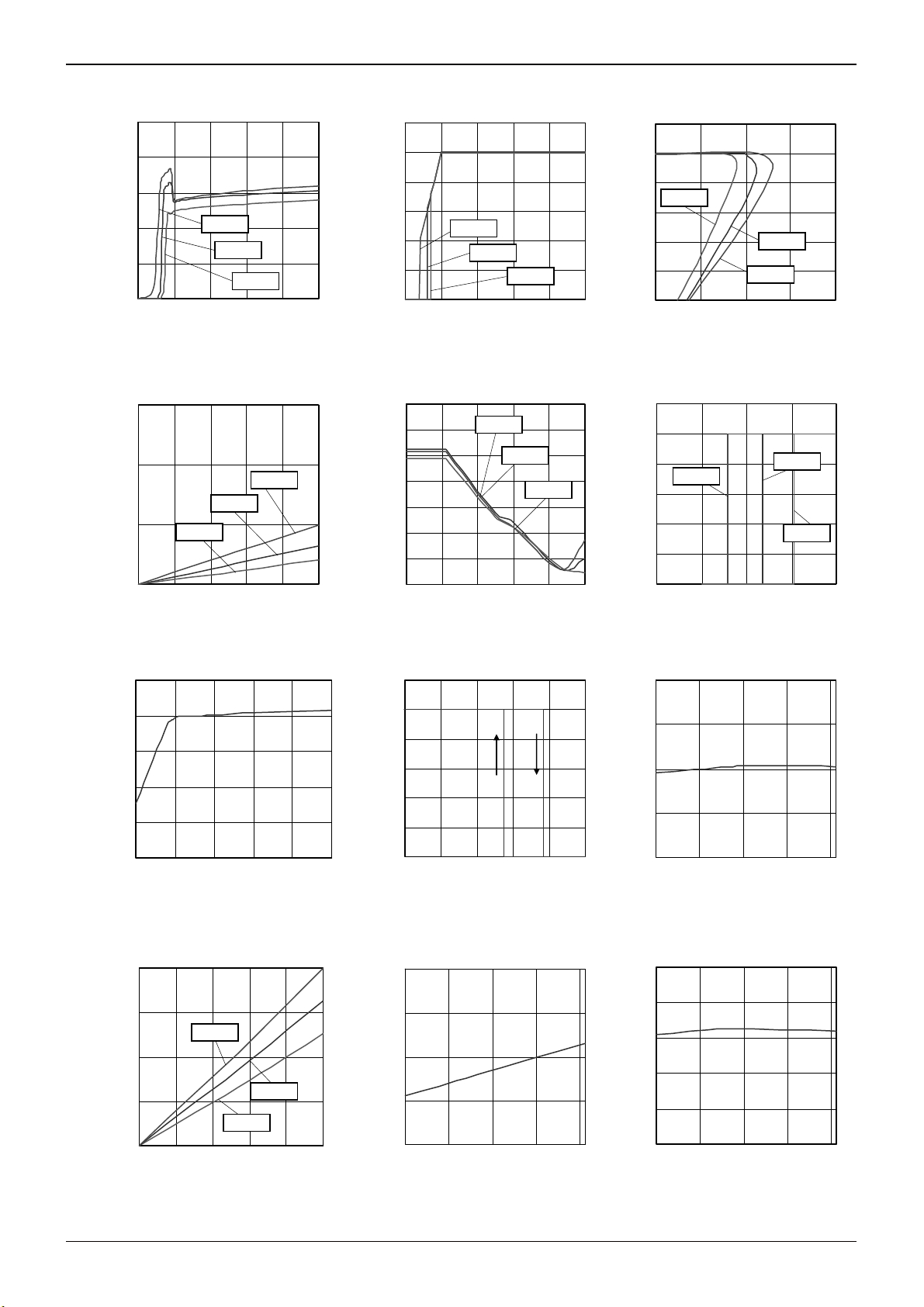
●Reference Data: BD3574HFP(Unless otherwise specified, Ta=25℃)
50
A]
40
μ
[
CC
30
20
10
CIRCUIT CURRENT: I
0
0 5 10 15 20 25
Ta=125℃
Ta=25℃
Ta=-40℃
SUPPLY VOLTAGE: V
[V]
CC
Fig. 1 Total Supply Current
3
Vd[V]
Δ
2
1
DROPOUT VOLTAGE:
0
Ta=-40℃
0 100 200 300 400 500
OUTPUT CURRENT: I
Ta=25℃
Ta=125℃
[mA]
O
Fig. 4 Dropout Voltage
100
A]
80
μ
[
CC
60
40
20
CIRCUIT CURRENT: I
0
0 100 200 300 400 500
OUTPUT CURRENT: I
O
[mA]
Fig. 7 Total Supply Current
Classified by Load
120
A]
μ
90
[
SW
60
30
SW BIAS CURRENT: I
0
0 5 10 15 20 25
Ta=125℃
Ta=-40℃
SUPPLY VOLTAGE: V
Ta=25℃
[V]
SW
Fig. 10 SW Bias current
6
5
[V]
O
4
3
2
OUTPUT VOLTAGE: V
1
0
0 5 10 15 20 25
Ta=125℃
Ta=25℃
SUPPLY VOLTAGE: V
Fig. 2 Output Voltage VS
Power Supply Voltage
70
60
[dB]
50
R.R.
40
30
20
RIPPLE REJECTION:
10
0
10 100 1000 10000 100000 1000000
Ta=125℃
Ta=25℃
FREQU ENC Y: f [Hz]
Fig. 5 Ripple rejection
6
5
[V]
O
4
3
2
OUTPUT VOLTAGE: V
1
0
100 120 140 160 180 200
AMBIEN T T EMPER ATU RE: T
Fig. 8 Thermal Shutdown Circuit
2
Vd [V]
1.5
Δ
1
0.5
DROPOUT VOLTAGE:
0
-40 0 40 80 120
AMBIEN T TEMPER ATURE: T
Fig. 11 Dropout voltage VS
Temperature
Ta=-40℃
CC
Ta=-40℃
Technical Note
6
5
[V]
O
4
Ta=-40℃
3
2
OUTPUT VOLTAGE: V
1
0
0 500 1000 1500 2000
[V]
OUTPUT CURRENT: I
Fig. 3 Output Voltage VS Load
6
5
[V]
O
4
Ta=125℃
3
2
OUTPUT VOLTAGE: V
1
0
00.511.52
SUPPLY VOLTAGE: V
Fig. 6 Output Voltage VS
SW Input Voltage
5.5
[V]
5.25
O
5
4.75
OUTPUT VOLTAGE: V
4.5
-40 0 40 80 120
[℃]
a
AMBIEN T TEMPER ATURE: T
Fig. 9 Output Voltage VS
Temperature
50
A]
40
μ
[
cc
30
20
10
CIRCUIT CURRENT: I
0
-40 0 40 80 12 0
[℃]
a
AMBIEN T TEMPER ATU RE: T
Fig. 12 Total Supply Current
Ta=25℃
Ta=125℃
O
Ta=25℃
[mA]
Ta=-40℃
[V]
SW
[℃]
a
[℃]
a
www.rohm.com
3/9
© 2011 ROHM Co., Ltd. All rights reserved.
2011.03 - Rev.B

BD3570FP/HFP, BD3571FP/HFP, BD3572FP/HFP, BD3573FP/HFP
1)
1)
BD3574FP/HFP, BD3575FP/HFP
●Block Diagram
Vcc
1
Cin
Vref
OCP
GND
Fin
TSD
2
Fig.13 TO252-3
N.C.
Vcc
1
Cin
SW
Vo
3
2
Co
GND
Fin
Vref
OCP
TSD
3
N.C.
Fig.14 TO252-5
Cin:0.33μF~1000μF
Co:0.1μF~1000μF
●I/O Circuit diagram (All resistance values are typical.)
SW
Fig.16 2PIN[SW]
●Pin Assignments
TO252-3
TO252-5
HRP5
210K
200K
1K
FIN
1 23
Fig. 19
FIN
234 5
1
Fig.20
FIN
12 3 45
Fig. 21
Pin No. Pin name Function
Pin No. Pin name Function
Vo
1992K: BD3570, BD3573
3706K: BD3571, BD3574
1250K
Fig.17 5PIN[VO]
BD3570,3571,3573,3574
1 VCC Power supply pin
2 N.C. N.C. pin
3 VO Voltage output pin
Fin GND GND pin
1 VCC Power supply pin
2
SW
N.C.
3 N.C. N.C. pin
4
N.C.
ADJ
5 VO Voltage output pin
Fin GND GND pin
Pin No. Pin name Function
1 VCC Power supply pin
2
SW
N.C.
3 GND GND pin
4
N.C.
ADJ
5 VO Voltage output pin
Fin GND GND pin
Technical Note
Vcc
1
Cin
SW
4
ADJ (N.C.
*1)
*2)
*
)
Vo
5
2
Co
GND
3
Fin
*1)For Fixed Voltage Regulator only
*2)For adjustable Voltage Regulator only
Vcc
Vo
150
Fig.18 4.5PIN[ADJ,VO]
BD3572,BD3575
V
O ON/OFF function pin
N.C. pin(BD3572FP only)
N.C. pin
Output voltage setting pin(BD3572,3575FP only)
V
O ON/OFF function pin (BD3573,3574,3575HFP only)
N.C. pin
N.C. pin
Output voltage setting pin(BD3572,3575HFP only)
Vref
OCP
TSD
Fig.15 HRP5
*1)
*2)
4
ADJ (N.C.
Vcc
*
)
Vo
5
Co
www.rohm.com
4/9
© 2011 ROHM Co., Ltd. All rights reserved.
2011.03 - Rev.B

BD3570FP/HFP, BD3571FP/HFP, BD3572FP/HFP, BD3573FP/HFP
A
A
A
BD3574FP/HFP, BD3575FP/HFP
Technical Note
●Output Voltage Adjustment
Vo
ADJ
R2
R1
Fig.22
To set the output voltage insert pull-down resistor R1 between the ADJ and GND pins,
and pull-up resistor R2 between the VO and ADJ pins.
Vo = VADJ×(R1+R2) / R1 [V]
{VADJ=1.26V(TYP.)}
The recommended connection resistor for the ADJ-GND is 30k~150kΩ.
●Setting of Heat
TO252-3 TO252-5 HRP5
2.0
1.6
1.2 W
1.2
0.8
IC mounted on a ROHM standard board
Substrate size: 70 mm 70 mm 1.6 mm
ja = 104.2 (°C/W)
2.0
1.6
1.2
0.8
1.3W
IC mounted on a ROHM standard board
Substrate size: 70 mm 70 mm 1.6 mm
ja = 96.2 (°C/W)
2.0
1.6
1.2
0.8
1.6 W
IC mounted on a ROHM standard board
Substrate size: 70 mm 70 mm 1.6 mm
ja = 78.1 (°C/W)
0.4
POWER DISSIPATION: Pd [W]
0
0
25 50 75 100 125 150
MBIENT TEMPERATURE: Ta [°C]
0.4
POWER DISSIPATION: Pd [W]
0
0
25 50 75 100 125 150
MBIENT TEMPERATURE: Ta [℃]
0.4
POWER DISSIPATION: Pd [W]
0
0
25 50 75 100 125 150
MBIENT TEMPERATURE: Ta [°C]
Fig. 23 Fig. 24 Fig. 25
Refer to the heat mitigation characteristics illustrated in Figs. 23, 24 and 25 when using the IC in an environment where Ta
≧25℃. The characteristics of the IC are greatly influenced by the operating temperature. If the temperature is in excess of
the maximum junction temperature T
jmax, the elements of the IC may be deteriorated or damaged. It is necessary to give
sufficient consideration to the heat of the IC in view of two points, i.e., the protection of the IC from instantaneous damage
and the maintenance of the reliability of the IC in long-time operation.
In order to protect the IC from thermal destruction, it is necessary to operate the IC not in excess of the maximum junction
temperature T
the IC within the power dissipation Pd. The following method is used to calculate the power consumption P
PC=(VCC-VO)×IO+VCC×ICC Vo : Output voltage
Power dissipation Pd≦PC Io : Load current
jmax. Fig. 23 illustrates the power dissipation/heat mitigation characteristics for the TO252 package. Operate
C (W).
Vcc : Input voltage
Icc : Total supply current
The load current I
Io≦
Pd-V
O is obtained to operate the IC within the power dissipation.
CC×ICC
CC-VO
V
(For more information about ICC, see page 12.)
The maximum load current Iomax for the applied voltage VCC can be calculated during the thermal design process.
●Calculation example
Example: BD3571FP V
I
0.624-12×ICC
IO≦
O≦89mA (ICC=30μA)
12-5
CC = 12 V and VO = 5 V at Ta = 85℃
θja=104.2℃/W→-9.6mAW/℃
25℃=1.2W→85℃=0.624W
Make a thermal calculation in consideration of the above so that the whole operating temperature range will be within the
power dissipation.
The power consumption Pc of the IC in the event of shorting (i.e., if the V
O and GND pins are shorted) will be obtained from
the following equation.
Pc=VCC×(ICC+Ishort) Ishort = Short current
www.rohm.com
5/9
© 2011 ROHM Co., Ltd. All rights reserved.
2011.03 - Rev.B

BD3570FP/HFP, BD3571FP/HFP, BD3572FP/HFP, BD3573FP/HFP
BD3574FP/HFP, BD3575FP/HFP
Technical Note
●Peripheral Settings for Pins and Precautions
1) V
CC pins
Insert capacitors with a capacitance of 0.33μF to 1000μF between the V
CC and GND pins.
The capacitance varies with the application. Be sure to design the capacitance with a sufficient margin.
2) Capacitors for stopping oscillation for output pins
Capacitors for stopping oscillation must be placed between each output pin and the GND pin. Use a capacitor within a
capacitance range between 0.1μF and 1000μF. Since oscillation does not occur even for ESR values from 0.001Ω to
100Ω, a ceramic capacitor can be used. Abrupt input voltage and load fluctuations can affect output voltages. Output
capacitor capacitance values should be determined after sufficient testing of the actual application.
●Operation Notes
1) Absolute maximum ratings
Use of the IC in excess of absolute maximum ratings such as the applied voltage or operating temperature range may
result in IC damage. Assumptions should not be made regarding the state of the IC (short mode or open mode) when
such damage is suffered. A physical safety measure such as a fuse should be implemented when use of the IC in a
special mode where the absolute maximum ratings may be exceeded is anticipated.
2) GND potential
Ensure a minimum GND pin potential in all operating conditions.
3) Setting of heat
Use a thermal design that allows for a sufficient margin in light of the power dissipation (Pd) in actual operating conditions.
4) Pin short and mistake fitting
Use caution when orienting and positioning the IC for mounting on printed circuit boards. Improper mounting may result in
damage to the IC. Shorts between output pins or between output pins and the power supply and GND pins caused by the
presence of a foreign object may result in damage to the IC.
5) Actions in strong magnetic field
Use caution when using the IC in the presence of a strong magnetic field as doing so may cause the IC to malfunction.
6) Testing on application boards
When testing the IC on an application board, connecting a capacitor to a pin with low impedance subjects the IC to stress.
Always discharge capacitors after each process or step. Be sure to turn power off when mounting or dismounting jigs at
the inspection stage. Furthermore, for countermeasures against static electricity, ground the equipment at the assembling
stage and pay utmost attention at the time of transportation or storing the product.
7) This monolithic IC contains P+ isolation and P substrate layers between adjacent elements in order to keep them isolated.
PN junction is formed by the P layer and the N layer of each element, and a variety of parasitic elements will be
constituted.
For example, when a resistor and transistor are connected to pins as shown in Fig. 19,
the P/N junction functions as a parasitic diode when GND>Pin A for the resistor or GND>Pin B for the transistor
(NPN).
Similarly, when GND>Pin B for the transistor (NPN), the parasitic diode described above combines with the N
layer of other adjacent elements to operate as a parasitic NPN transistor.
www.rohm.com
6/9
© 2011 ROHM Co., Ltd. All rights reserved.
2011.03 - Rev.B

BD3570FP/HFP, BD3571FP/HFP, BD3572FP/HFP, BD3573FP/HFP
t
)
r
)
BD3574FP/HFP, BD3575FP/HFP
Technical Note
The formation of parasitic elements as a result of the relationships of the potentials of different pins is an inevitable result of
the IC's architecture. The operation of parasitic elements can cause interference with circuit operation as well as IC
malfunction and damage. For these reasons, it is necessary to use caution so that the IC is not used in a way that will
trigger the operation of parasitic elements, such as by the application of voltages lower than the GND (P substrate) voltage
to input pins.
(Pin A)
P+
N
N
P
Resistor
N
P
GND
P+
Parasitic element
(Pin B
NN
Parasitic elemen
or transistor
Transistor (NPN)
C
P+
B
N
P
substr
E
P
GND
P+
(Pin B
C
B
E
(Pin A)
GND
Parasitic element o
transistor
Parasitic elements
Fig. 26 Example of a Simple Monolithic IC Architecture
8) Ground wiring patterns
When using both small signal and large current GND patterns, it is recommended to isolate the two ground patterns,
placing a single ground point at the application's reference point so that the pattern wiring resistance and voltage
variations caused by large currents do not cause variations in the small signal ground voltage. Be careful not to change
the GND wiring pattern of any external parts, either.
9) SW Pin
Do not apply the voltage to SW pin when the V
And when the V
CC is applied, the voltage of SW pin must not exceed VCC.
CC is not applied.
10) Thermal shutdown circuit (TSD)
This IC incorporates a built-in thermal shutdown circuit for the protection from thermal destruction. The IC should be used
within the specified power dissipation range. However, in the event that the IC continues to be operated in excess of its
power dissipation limits, the attendant rise in the chip's temperature T
all output power elements. The circuit automatically resets once the chip's temperature T
j will trigger the thermal shutdown circuit to turn off
j drops.
The thermal shutdown circuit operates if the IC is under conditions in express of the absolute maximum ratings. Never
design sets on the premise of using the thermal shutdown circuit. (See Fig. 8)
11) Overcurrent protection circuit (OCP)
The IC incorporates a built-in overcurrent protection circuit that operates according to the output current capacity. This
circuit serves to protect the IC from damage when the load is shorted. The protection circuit is designed to limit current
flow by not latching in the event of a large and instantaneous current flow originating from a large capacitor or other
component. These protection circuits are effective in preventing damage due to sudden and unexpected accidents.
However, the IC should not be used in applications characterized by the continuous operation or transitioning of the
protection circuits. At the time of thermal designing, keep in mind that the current capability has negative characteristics to
temperatures. (See Fig. 3)
www.rohm.com
7/9
© 2011 ROHM Co., Ltd. All rights reserved.
2011.03 - Rev.B

BD3570FP/HFP, BD3571FP/HFP, BD3572FP/HFP, BD3573FP/HFP
BD3574FP/HFP, BD3575FP/HFP
●Ordering Part Number
B D 3 5 7 4 H F P - T R
Part number
3570:3.3V output
no include SW
3571:5.0V output
no include SW
3572:variable output
no include SW
3573:3.3V output
include SW
3574:5.0V output
include SW
3575:variable output
include SW
6.5±0.2
C0.5
+0.2
5.1
-
5.5±0.2 1.5±0.2
2.3±0.2
5.5±0.2 1.5±0.2
0.65
0.75
123 54
0.5
FIN
0.8
6.5±0.2
+0.2
5.1
-
FIN
0.1
21 3
0.1
0.8
0.65
2.3±0.2
C0.5
1.27
2.3±0.2
2.3±0.2
0.5±0.1
0.5±0.1
1.0±0.2
0.5±0.1
1.0±0.2
1.5
0.5±0.1
1.5
2.5
2.5
9.5±0.5
(Unit : mm)
9.5±0.5
(Unit : mm)
Package
FP : TO252-3,
TO252-5
HFP: HRP5
<Tape and Reel information>
Embossed carrier tapeTape
Quantity
Direction
of feed
<Tape and Reel information>
Quantity
Direction
of feed
2000pcs
E2
The direction is the 1pin of product is at the lower left when you hold
( )
reel on the left hand and you pull out the tape on the right hand
Reel
Embossed carrier tapeTape
2000pcs
E2
The direction is the 1pin of product is at the lower left when you hold
( )
reel on the left hand and you pull out the tape on the right hand
Reel
Packaging and forming
specification
E2: Embossed tape and reel
(TO252-3,TO252-5)
TR: Embossed tape and reel
(HRP5)
1pin
Order quantity needs to be multiple of the minimum quantity.
∗
1pin
Order quantity needs to be multiple of the minimum quantity.
∗
ローム形名
TO252-3
TO252-5
Technical Note
Direction of feed
Direction of feed
www.rohm.com
8/9
© 2011 ROHM Co., Ltd. All rights reserved.
2011.03 - Rev.B

BD3570FP/HFP, BD3571FP/HFP, BD3572FP/HFP, BD3573FP/HFP
BD3574FP/HFP, BD3575FP/HFP
HRP5
9.395±0.125
(MAX 9.745 include BURR)
8.82 ± 0.1
(6.5)
8.0±0.13 1.017±0.2
1.2575
1.72
0.08±0.05
54321
0.73±0.1
0.08 S
(7.49)
1.905±0.1
S
0.835±0.2
1.523±0.15
+5.5°
4.5°
−4.5°
+0.1
0.27
−0.05
(Unit : mm)
10.54±0.13
<Tape and Reel information>
Quantity
Direction
of feed
Technical Note
Embossed carrier tapeTape
2000pcs
TR
The direction is the 1pin of product is at the upper right when you hold
( )
reel on the left hand and you pull out the tape on the right hand
1pin
Direction of feed
Reel
Order quantity needs to be multiple of the minimum quantity.
∗
www.rohm.com
9/9
© 2011 ROHM Co., Ltd. All rights reserved.
2011.03 - Rev.B

Notes
No copying or reproduction of this document, in part or in whole, is permitted without the
consent of ROHM Co.,Ltd.
The content specied herein is subject to change for improvement without notice.
The content specied herein is for the purpose of introducing ROHM's products (hereinafter
"Products"). If you wish to use any such Product, please be sure to refer to the specications,
which can be obtained from ROHM upon request.
Examples of application circuits, circuit constants and any other information contained herein
illustrate the standard usage and operations of the Products. The peripheral conditions must
be taken into account when designing circuits for mass production.
Great care was taken in ensuring the accuracy of the information specied in this document.
However, should you incur any damage arising from any inaccuracy or misprint of such
information, ROHM shall bear no responsibility for such damage.
The technical information specied herein is intended only to show the typical functions of and
examples of application circuits for the Products. ROHM does not grant you, explicitly or
implicitly, any license to use or exercise intellectual property or other rights held by ROHM and
other parties. ROHM shall bear no responsibility whatsoever for any dispute arising from the
use of such technical information.
The Products specied in this document are intended to be used with general-use electronic
equipment or devices (such as audio visual equipment, ofce-automation equipment, communication devices, electronic appliances and amusement devices).
The Products specied in this document are not designed to be radiation tolerant.
While ROHM always makes efforts to enhance the quality and reliability of its Products, a
Product may fail or malfunction for a variety of reasons.
Please be sure to implement in your equipment using the Products safety measures to guard
against the possibility of physical injury, re or any other damage caused in the event of the
failure of any Product, such as derating, redundancy, re control and fail-safe designs. ROHM
shall bear no responsibility whatsoever for your use of any Product outside of the prescribed
scope or not in accordance with the instruction manual.
The Products are not designed or manufactured to be used with any equipment, device or
system which requires an extremely high level of reliability the failure or malfunction of which
may result in a direct threat to human life or create a risk of human injury (such as a medical
instrument, transportation equipment, aerospace machinery, nuclear-reactor controller, fuelcontroller or other safety device). ROHM shall bear no responsibility in any way for use of any
of the Products for the above special purposes. If a Product is intended to be used for any
such special purpose, please contact a ROHM sales representative before purchasing.
If you intend to export or ship overseas any Product or technology specied herein that may
be controlled under the Foreign Exchange and the Foreign Trade Law, you will be required to
obtain a license or permit under the Law.
Notice
www.rohm.com
© 2011 ROHM Co., Ltd. All rights reserved.
Thank you for your accessing to ROHM product informations.
More detail product informations and catalogs are available, please contact us.
ROHM Customer Support System
http://www.rohm.com/contact/
R1120
A
 Loading...