

Page 1
Hi-performance Regulator IC Series for PCs
Nch FET Ultra LDOs
for Desktop PCs Chipsets with Power Good
BD3540NUV, BD3541NUV
●Description
The BD3540NUV, BD3541NUV low-voltage output linear 1ch series chipset regulator IC operates from a very low input
supply, and offers ideal performance in low input voltage to low output voltage applications. It incorporates a built-in
N-MOSFET power transistor to minimize the input-to-output voltage differential to the ON resistance (R
400mΩ) level. By lowering the dropout voltage in this way, the regulator realizes high current output (Iomax=0.5A~1.0A)
with reduced conversion loss, and thereby obviates the switching regulator and its power transistor, choke coil, and rectifier
diode. Thus, the BD3540NUV, BD3541NUV are designed to enable significant package profile downsizing and cost
reduction. An external resistor allows the entire range of output voltage configurations between 0.65 and 2.7V, while the
NRCS (soft start) function enables a controlled output voltage ramp-up, which can be programmed to whatever power
supply sequence is required.
●Features
1) High-precision voltage regulator(0.65V±1%)
2) Built-in VCC undervoltage lockout circuit
3) NRCS (soft start) function reduces the magnitude of in-rush current
4) Internal Nch MOSFET driver offers low ON resistance
5) Built-in current limit circuit
6) Built-in thermal shutdown (TSD) circuit
7) Variable output
8) Small package VSON010V3030 : 3.0×3.0×1.0(mm)
9) Tracking function
●Applications
Notebook computers, Desktop computers, LCD-TV, DVD, Digital appliances
●Line-up
It is available to select power supply voltage and maximum output voltage.
Maximum Output Voltage Package Vcc=5V
0.5A
1.0A BD3541NUV
VSON010V3030
BD3540NUV
No.09030EBT04
ON=200mΩ~
www.rohm.com
© 2009 ROHM Co., Ltd. All rights reserved.
1/16
2009.04 - Rev.B
Page 2
BD3540NUV, BD3541NUV
Technical Note
●Absolute maximum ratings
◎BD3540NUV, BD3541NUV
Parameter Symbol
BD3540NUV BD3541NUV
Limit
Unit
Input Voltage 1 VCC +6.0 *1 V
Input Voltage 2 VIN +6.0 *1 V
Enable Input Voltage Ven -0.3~+6.0 V
PGOOD Input Voltage V
+6.0*1 V
PGOOD
Power Dissipation 1 Pd1 0.70*2 W
Power Dissipation 2 Pd2 1.27*2 W
Power Dissipation 3 Pd3 3.03*2 W
Operating Temperature Range Topr -10~+100 ℃
Storage Temperature Range Tstg -55~+150 ℃
Junction Temperature Tjmax +150 ℃
*1 Should not exceed Pd.
*2 Reduced by 5.6mW/℃ for each increase in Ta≧25℃ (when mounted on a 74.2mm×74.2mm×1.6mm glass-epoxy board, 1-layer)
On less than 0.2% (percentage occupied by copper foil.
*3 Reduced by 10.1mW/℃ for each increase in Ta≧25℃ (when mounted on a 74.2mm×74.2mm×1.6mm glass-epoxy board, 1-layer)
On less than 7.0% (percentage occupied by copper foil.
*4 Reduced by 24.2mW/℃ for each increase in Ta≧25℃ (when mounted on a 74.2mm×74.2mm×1.6mm glass-epoxy board, 1-layer)
On less than 65.0% (percentage occupied by copper foil.
●Operating Voltage(Ta=25℃)
◎BD3540NUV, BD3541NUV
Parameter Symbol Min. Max. Unit
Input Voltage 1 VCC 3.0 5.5 V
Input Voltage 2 VIN 0.95 VCC-1
Output Voltage IO -
PGOOD Input Voltage V
-0.3 5.5 V
PGOOD
BD3540NUV BD3541NUV
0.5 1.0
*1*5
V
A
Output Voltage Setting Range Vo VFB 2.7 V
Enable Input Voltage Ven 0 5.5 V
*5 VCC and VIN do not have to be implemented in the order listed.
*This product is not designed for use in radioactive environments.
●Attention : About this document
The official specification of this product (BD354XNUV) is the Japanese version.
This translation is intended only as a reference to understand the official version.
If there are any differences between the Japanese and this translated version, the official Japanese version takes priority.
www.rohm.com
© 2009 ROHM Co., Ltd. All rights reserved.
2/16
2009.04 - Rev.B
Page 3

BD3540NUV, BD3541NUV
Technical Note
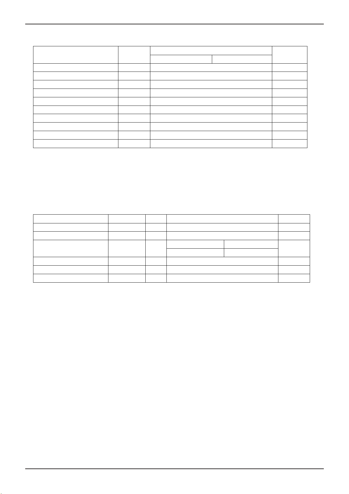
●Electrical Characteristics
(Unless otherwise specified, Ta=25℃, VCC=5V, Ven=3V, VIN=1.7V, R1=3.9KΩ, R2=3.3KΩ)
Parameter Symbol
Bias Current
VCC Shutdown Mode Current
Output Voltage
Output Voltage Temperature
Coefficient
Feedback Voltage 1
Feedback Voltage 2
Load Regulation
Line Regulation 1
Line Regulation 2
Standby Discharge Current
ICC
IST
VOUT
Tcvo
VFB1
VFB2
Reg.L
Reg.l1
Reg.l2
Iden
Min. Typ. Max.
- 0.7 1.0 mA
- 0 10 μA
- 1.200 - V
- 0.01 - %/℃
0.643 0.650 0.657 V
0.637 0.650 0.663 V
- 0.5 10 mV
- 0.1 0.5 %/V
- 0.1 0.5 %/V
1 - - mA
Limit
Unit Condition
Ven=0V
Tj=-10 to 100℃
(BD3540NUV Io=0A to 0.5A)
(BD3541NUV Io=0A to 1.0A)
VCC=3.0V to 5.5V
VIN=1.5V to 3.3V
Ven=0V, Vo=1V
[ENABLE]
Enable Pin
Input Voltage High
Enable PinInput Voltage Low
Enable Input Bias Current
Enhi
Enlow
Ien
2 - - V
0 - VCC×0.15 V
- 7 10 μA
Ven=3V
[NRCS]
NRCS Charge Current
NRCS Standby Voltage
Inrcs 14 20 26 μA Vnrcs=0.5V
VSTB - 0 50 mV Ven=0V
[UVLO]
VCC Undervoltage Lockout
Threshold Voltage
VCC Undervoltage Lockout
Hysteresis Voltage
VccUVLO 2.3 2.5 2.7 V Vcc:Sweep-up
Vcchys 50 100 150 mV Vcc:Sweep-down
[PGOOD]
Low-side Threshold Voltage V
High-side Threshold Voltage V
PGDLY charge current I
VO×0.87 VO×0.9 VO×0.93 V
THPGL
VO×1.07 VO×1.1 VO×1.13 V
THPGL
1.4 2.0 2.6 μA
PGDLY
Ron RPG 30 75 150 Ω
[AMP]
Io=0.5A, VIN=1.2V,
Ta=-10 to 100℃
Io=1.0A, VIN=1.2V,
Ta=-10 to 100℃
Minimum
dropout voltage
BD3540NUV dVo - 200 300 mV
BD3541NUV dvo - 200 300 mV
www.rohm.com
© 2009 ROHM Co., Ltd. All rights reserved.
3/16
2009.04 - Rev.B
Page 4
BD3540NUV, BD3541NUV
v
v
v
v
v
v
v
v
v
v
v
v
v
v
v
v
v
μ
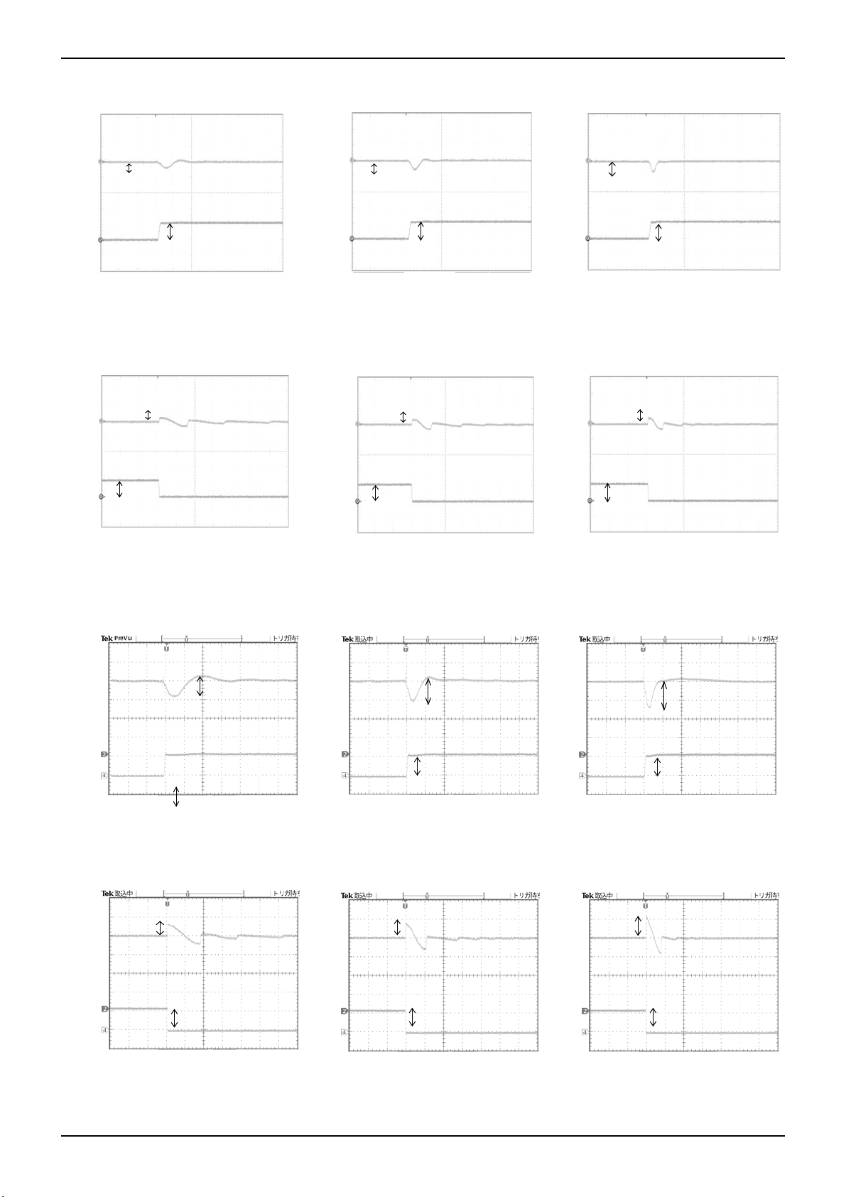
●Reference Data(BD3540NUV)
Technical Note
50mV/di
0.5A/di
50mV/di
0.5A/di
Vo
13mV
Io
Io=0A→1A/μsec t(10μsec/div)
0.5A
Fig.1 Transient Response
(0→0.5A)
Co=100μF, Cfb=1000pF
Vo
13mV
Io
0.5A
Io=1A→0A/μsec t(100μsec/div)
Fig.4 Transient Response
(0.5→0A)
=
Vo
50mV/di
0.5A/di
29mV
Io
Io=0A→1A/μsec t(10μsec/div)
0.5A
Fig.2 Transient Response
(0→0.5A)
50mV/div
0.5A/div
Co=47μF, Cfb=1000pF
Vo
25mV
Io
0.5A
Io=1A→0A/μsec t(100μsec/div)
Fig.5 Transient Response
(0.5→0A)
=
μF, Cfb=1000pF
Co=47
50mV/di
0.5A/di
50mV/div
0.5A/div
Vo
Io
38mV
0.5A
Io=0A→1A/μsec t(10μsec/div)
Fig.3 Transient Response
(0→0.5A)
=
Vo
35mV
0.5A
Io
Io=1A→0A/μsec t(100μsec/div)
=
Fig.6 Transient Response
(0.5→0A)
Co=22μF, Cfb=1000pF
●Reference Data(BD3541NUV)
Vo
50mV/di
Io
1A/di
42mV
1.0A
Fig.7 Transient Response
(0→1.0A)
Co=100μF, Cfb=1000pF
42mV
Vo
50mV/di
Io
1A/di
1.0A
50mV/div
1A/div
50mV/di
1A/di
Vo
Io
1.0A
Fig.8 Transient Response
(0→1.0A)
Co=47
51mV
Vo
Io
F, Cfb=1000pF
1.0A
53mV
50mV/di
1A/di
50mV/di
1A/div
Vo
59mV
Io
1.0A
Fig.9 Transient Response
(0→1.0A)
Co=22μF, Cfb=1000pF
57mV
Vo
Io
1.0A
www.rohm.com
© 2009 ROHM Co., Ltd. All rights reserved.
Fig.10 Transient Response
(1.0→0A)
Co=100
μF, Cfb=1000pF
Fig.11 Transient Response
(1.0→0A)
Co=47μF, Cfb=1000pF
4/16
Fig.12 Transient Response
(1.0→0A)
Co=22μF, Cfb=1000pF
2009.04 - Rev.B
Page 5
BD3540NUV, BD3541NUV
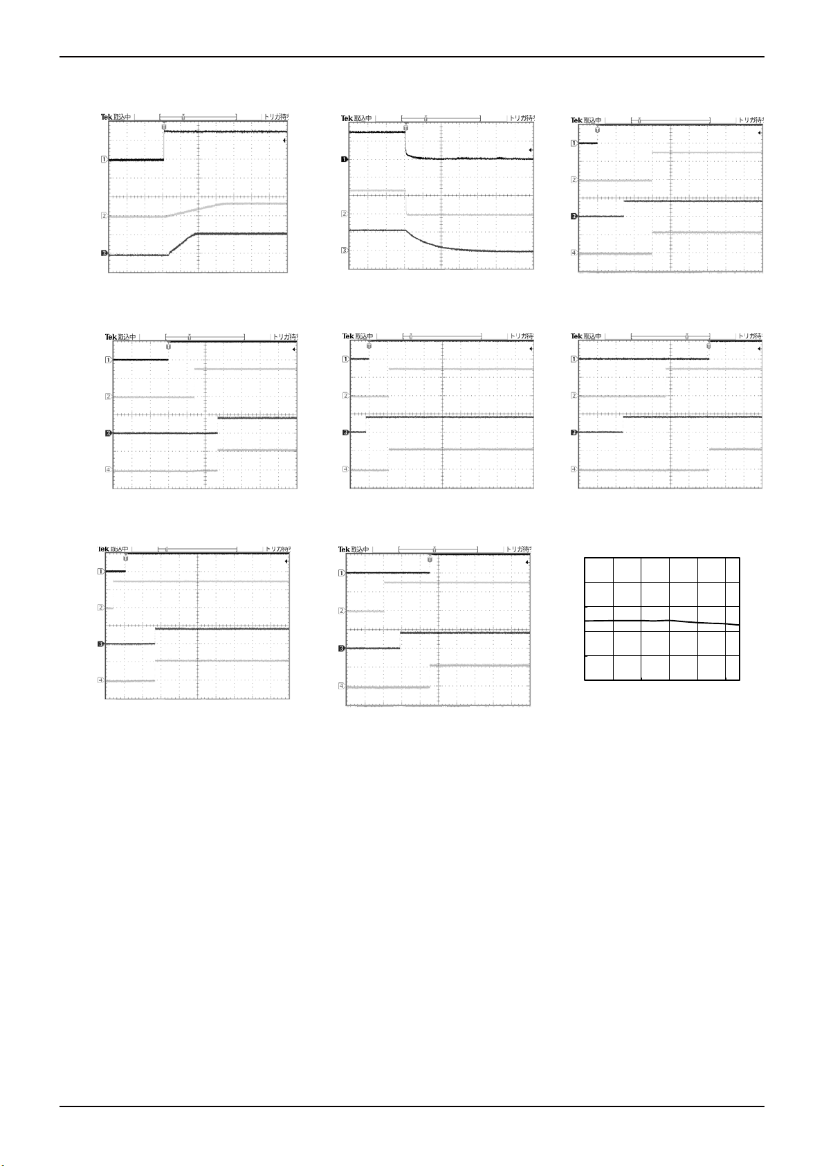
●Reference Data(BD3540NUV)
Technical Note
VCC
VCC
Ven
Ven
VIN
VIN
Fig.19 Waveform at output
Fig.20 Waveform at output OFF
VCC
Ven
VIN
Vo
Fig.21 Input sequence
VCC
Ven
VIN
Vo
VCC
Ven
VIN
Vo
VCC
Ven
VIN
Vo
Fig.22 Input sequence
Fig.23 Input sequence
Fig.24 Input sequence
1.25
VCC
VCC
1.23
Ven
VIN
Vo
Fig.25 Input sequence
VIN→Ven →VCC Ven→VIN→VCC
Ven
VIN
Vo
Fig.26 Input sequence
1.21
Vo(V)
1.19
1.17
1.15
-101030507090
Ta(℃)
Fig.27 Ta-Vo (Io=0mA)
www.rohm.com
© 2009 ROHM Co., Ltd. All rights reserved.
5/16
2009.04 - Rev.B
Page 6
BD3540NUV, BD3541NUV
IIN ( u A )
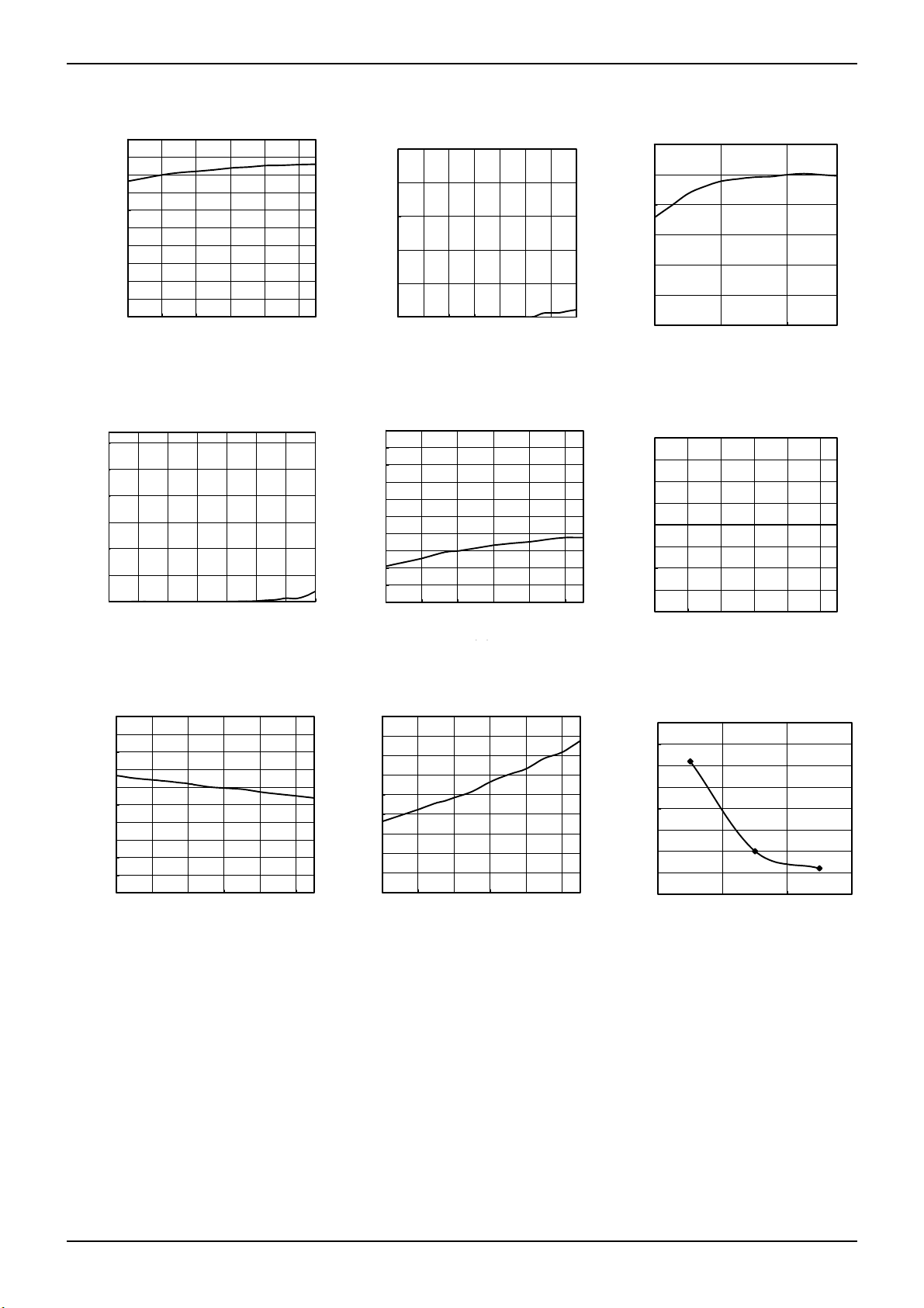
●Reference Data(BD3540NUV)
Technical Note
0.70
0.65
0.60
0.55
0.50
0.45
ICC(mA)
0.40
0.35
0.30
0.25
0.20
-10 10 30 50 70 90
Ta(℃)
Fig.28 Ta-ICC
30
25
20
15
10
5
0
-60 -30 0 30 60 90 120 150
Fig.31 Ta-IINSTB
Ta(℃)
100
100
0.10
0.08
0.06
0.04
ICC(uA)
0.02
0.00
-60 -30 0 30 60 90 120 150
Ta(℃)
Fig.29 Ta-ISTB
25
25
25
24
24
24
23
23
23
22
22
22
21
21
21
20
20
20
19
19
INRCS(uA)
19
INRCS(uA)
INRCS(uA)
18
18
18
17
17
17
16
16
16
15
15
15
-101030507090
-101030507090
-101030507090
Ta(℃)
Ta(℃)
Ta(℃)
Fig.32 Ta-INRCS
100
100
1.70
1.65
1.60
1.55
IIN(mA)
1.50
1.45
1.40
-10 30 70
Ta(℃)
Fig.30 Ta-IIN
20
20
15
15
10
10
5
5
0
0
IFB(nA)
IFB(nA)
-5
-5
-10
-10
-15
-15
-20
-20
-10 10 30 50 70 90
-10 10 30 50 70 90
Ta(℃)
Ta(℃)
Fig.33 Ta-IFB
100
100
100
10
10
9
9
8
8
7
7
6
6
5
5
Ien(uA)
4
Ien(uA)
4
3
3
2
2
1
1
0
0
-101030507090
-101030507090
Ta(℃)
Ta(℃)
Fig.34 Ta-Ien
100
100
180
150
170
170
160
140
160
150
150
130
)
)
)
140
Ω
140
Ω
Ω
120
130
130
RON(m
RON(m
RON(m
120
120
110
110
110
100
100
100
90
90
90
-101030507090
-10 10 30 50 70 90
-1010305070 90
Ta(℃)
Ta(℃)
Ta(℃)
Fig.35 Ta-RON
(VCC=5V/Vo=1.2V)
100
100
200
190
180
)
170
Ω
160
RON(m
150
140
130
120
2468
Vcc(V)
Fig.36 VCC-RON
www.rohm.com
© 2009 ROHM Co., Ltd. All rights reserved.
6/16
2009.04 - Rev.B
Page 7

BD3540NUV, BD3541NUV
C
V
V
V
Y
V
Technical Note
●Block Diagram
2
CC
1
Reference
Block
C1
UVLO
Current
CLEN
Limit
CC
IN
5
IN
C2
NRCS
CL
UVLO
TSD
EN
Power
Good
Thermal
Shutdown
TSD
Vo
6
7
R1
Vo
8
FB
R2
Vo
C
FB
C3
NRCS
9
NRCS
C
10
GND
4
C
PGDL
PGDLY
3
PG
●Pin Function Table
PIN No. PIN name PIN Function
1 VCC Power supply pin
2 EN Enable input pin
3 PG Power Good pin
4 PGDLY Power Good Delay capacitor connection pin
5 VIN Input voltage pin
6 VO Output voltage pin
7 VO Output voltage pin
8 FB Reference voltage feedback pin
9 NRCS In-rush current protection (NRCS) capacitor connection pin
10 GND Ground pin
●Pin Layout
◎VSON010V3030
0.1
±
3.0
1.0Max.
0.08 S
Lot No.
3.0±0.1
B D 3
5 4 ×
+0.03
2.0±0.1
15
Lot No.
-0.02
0.02
S
(0.22)
0.25
0.4±0.1
0.5
0.5
610
0.25
1.2±0.1
+0.05
-0.04
(Unit : mm)
www.rohm.com
© 2009 ROHM Co., Ltd. All rights reserved.
7/16
2009.04 - Rev.B
Page 8

BD3540NUV, BD3541NUV
pgdly
(μA)
●Operation of Each Block
・AMP
This is an error amp that compares the reference voltage (0.65V) with Vo to drive the output Nch FET (Ron=100mΩ~
400mΩ). Frequency optimization helps to realize rapid transient response, and to support the use of ceramic capacitors
on the output. AMP input voltage ranges from GND to 2.7V, while the AMP output ranges from GND to VCC. When EN is
OFF, or when UVLO is active, output goes LOW and the output of the NchFET switches OFF.
・EN
The EN block controls the regulator’s ON/OFF state via the EN logic input pin. In the OFF position, circuit voltage is
maintained at 0μA, thus minimizing current consumption at standby. The FET is switched ON to enable discharge of the
NRCS pin Vo, thereby draining the excess charge and preventing the IC on the load side from malfunctioning. Since no
electrical connection is required (e.g., between the VCC pin and the ESD prevention Diode), module operation is
independent of the input sequence.
・UVLO
To prevent malfunctions that can occur during a momentary decrease in VCC, the UVLO circuit switches the output OFF,
and (like the EN block) discharges NRCS and Vo. Once the UVLO threshold voltage (TYP2.5V) is reached, the power-on
reset is triggered and output continues.
・CURRENT LIMIT
When output is ON, the current limit function monitors the internal IC output current against the parameter value (2.0A or
more:BD3540NUV). When current exceeds this level, the current limit module lowers the output current to protect the
load IC. When the overcurrent state is eliminated, output voltage is restored to the parameter value.
・NRCS (Non Rush Current on Start-up)
The soft start function enabled by connecting an external capacitor between the NRCS pin and ground. Output ramp-up
can be set for any period up to the time the NRCS pin reaches VFB (0.65V). During startup, the NRCS pin serves as a
20μA (TYP) constant current source to charge the external capacitor. Output start time is calculated via formula (1) below.
t = C ・・・(1)
Tracking sequence is available by connecting the output voltage of external power supply instead of external capacitor.
And then, ratio-metric sequence is also available by changing the resistor division ratio of external power supply output
voltage. (See the next page)
・TSD (Thermal Shut down)
The shutdown (TSD) circuit automatically switches output OFF when the chip temperature gets too high, thus serving to
protect the IC against “thermal runaway” and heat damage. Because the TSD circuit is provided to shut down the IC in
the presence of extreme heat, in order to avoid potential problems with the TSD, it is crucial that the Tj (max) parameter
not be exceeded in the thermal design.
・VIN
The VIN line acts as the major current supply line, and is connected to the output NchFET drain. Since no electrical
connection (such as between the VCC pin and the ESD protection Diode) is necessary, VIN operates independent of the
input sequence. However, since an output NchFET body Diode exists between VIN and Vo, a VIN-Vo electric (Diode)
connection is present. Note, therefore, that when output is switched ON or OFF, reverse current may flow to VIN from Vo.
・PGOOD
It outputs the output voltage (Vo). PGOOD pin (open drain) is used to pull up the 100kΩ resistor. PGOOD will be
judged HIGH between the FB voltage 0.585V(TYP) to 0.715V(TYP), and will be judged LOW if the voltage is out of range.
・PGDLY
It is available to set PGOOD output delay. PGDLY pin should be connected to 100pF capacitor.
PGOOD delay time id determined by the following formula.
C(pF)×0.75
= (μsec)
t
pgdly
I
Technical Note
0.65V
20μA
www.rohm.com
© 2009 ROHM Co., Ltd. All rights reserved.
8/16
2009.04 - Rev.B
Page 9

BD3540NUV, BD3541NUV
●Timing Chart
EN ON/OFF
VIN
VCC
EN
NRCS
Vo
PGOOD
VCC ON/OFF
VIN
VCC
EN
NRCS
Vo
PGOOD
Tracking sequence
1.7V Output
1.2V Output
(R
=3.9kΩ, R2=3.3kΩ)
1
Tracking sequence
1.7V
1.2V
Ratio-metric sequence
0.65V(typ)
Vo×0.9V(typ)
UVLO
0.65V(typ)
Startup
Star tup
40μs (typ@100pF)
DC/DC
40uS(typ@ C=100pF)
1.7V
Vo
R2
R
1
Hysteresis
Technical Note
t
t
NRCS
V0
FB
1.2V
3.3kΩ
3.9kΩ
www.rohm.com
© 2009 ROHM Co., Ltd. All rights reserved.
9/16
2009.04 - Rev.B
Page 10

BD3540NUV, BD3541NUV
●Evaluation Board
BD354XNUV Evaluation Board Schematic
■■
Technical Note
BD354XNUV
BD354XNUV Evaluation Board Standard Component List
■■
Component Rating Manufacturer Product Name Component Rating Manufacturer Product Name
U1 - ROHM BD354XNUV C2 22uF KYOCERA CM32X5R226M10A
C1 1uF MURATA GRM188B11A105KD C13 1000pF MURATA GRM188B11H102KD
C10 0.01uF MURATA GRM188B11H103KD R1 3.9kΩ ROHM MCR03EZPF3301
R8 0Ω - Jumper R2 3.3kΩ ROHM MCR03EZPF3901
C5 22uF KYOCERA CM32X5R226M10A R4 100kΩ ROHM MCR03EZPF
BD354XNUV Evaluation Board Layout
■■
(2nd layer and 3rd layer are GND Line.)
www.rohm.com
© 2009 ROHM Co., Ltd. All rights reserved.
TOP Layer
10/16
Bottom Layer Silkscreen
2009.04 - Rev.B
Page 11

BD3540NUV, BD3541NUV
Technical Note
●Recommended Circuit Example
VCC
EN
VCC
C6
VIN
Component
Recommended
Val ue
R1/R2 3.9k/3.3k
C3 22μF
C1 1μF
C2 22μF
C4 0.01μF
R4
R5
C1
C2
1
2
3
4
5
10
9
8
7
6
R2
R1
GND
C4
FB
C5
VOUT1(1.2V)
C3
Programming Notes and Precautions
IC output voltage can be set with a configuration formula using the values for the internal
reference output voltage (V
values that will avoid the impact of the VREF
)and the output voltage resistors (R1, R2). Select resistance
FB
current (±100nA). The recommended total
resistance value is 10KΩ.
To assure output voltage stability, please be certain the VOUT1 pins and the GND pins are
connected. Output capacitors play a role in loop gain phase compensation and in
mitigating output fluctuation during rapid changes in load level. Insufficient capacitance
may cause oscillation, while high equivalent series reisistance (ESR) will exacerbate
output voltage fluctuation under rapid load change conditions. While a 22μF ceramic
capacitor is recomended, actual stability is highly dependent on temperature and load
conditions. Also, note that connecting different types of capacitors in series may result in
insufficient total phase compensation, thus causing oscillation. In light of this information,
please confirm operation across a variety of temperature and load conditions.
Input capacitors reduce the output impedance of the voltage supply source connected to
the (VCC) input pins. If the impedance of this power supply were to increase, input voltage
(VCC) could become unstable, leading to oscillation or lowered ripple rejection function.
While a low-ESR 1μF capacitor with minimal susceptibility to temperature is
recommended, stability is highly dependent on the input power supply characteristics and
the substrate wiring pattern. In light of this information, please confirm operation across a
variety of temperature and load conditions.
Input capacitors reduce the output impedance of the voltage supply source connected to
the (VIN) input pins. If the impedance of this power supply were to increase, input voltage
(VIN) could become unstable, leading to oscillation or lowered ripple rejection function.
While a low-ESR 22μF capacitor with minimal susceptibility to temperature is
recommended, stability is highly dependent on the input power supply characteristics and
the substrate wiring pattern. In light of this information, please confirm operation across a
variety of temperature and load conditions.
The Non Rush Current on Startup (NRCS) function is built into the IC to prevent rush
current from going through the load (VIN to VO) and impacting output capacitors at power
supply start-up. Constant current comes from the NRCS pin when EN is HIGH or the UVLO
function is deactivated. The temporary reference voltage is proportionate to time, due to
the current charge of the NRCS pin capacitor, and output voltage start-up is proportionate
to this reference voltage. Capacitors with low susceptibility to temperature are
recommended, in order to assure a stable soft-start time.
C5
-
This component is employed when the C3 capacitor causes, or may cause, oscillation. It
provides more precise internal phase correction.
R5 100k It is pull-up resistance of Open Drain pin. 100kΩ is recommended.
R4
www.rohm.com
© 2009 ROHM Co., Ltd. All rights reserved.
Several kΩ
~several 10kΩ
It is recommended that a resistance (several kΩ to several 10kΩ) be put in R4, in case
negative voltage is applied in EN pin.
11/16
2009.04 - Rev.B
Page 12

BD3540NUV, BD3541NUV
●Input-Output Equivalent Circuit Diagram
VCC
VCC
Technical Note
NRCS
1kΩ
1kΩ
10kΩ
VO1
VO2
●Reference landing pattern
VCC
50kΩ
Lead pitch
0.65 2.50 0.40 0.35
central pad length
3.00 1.90
*It is recommended to design suitable for the actual application.
1kΩ
1kΩ
EN
10kΩ
b2
L2
D3
1kΩ
VIN
10kΩ
VCC
VFB
100kΩ
100kΩ
20pF
MIE
E3
1kΩ
1kΩ
1kΩ
1kΩ
e
(Unit : mm)
Lead pitch
e
MIE
landing length
≧l2
landing pitch
b2
central pad pitch
D3 E3
350kΩ
www.rohm.com
© 2009 ROHM Co., Ltd. All rights reserved.
12/16
2009.04 - Rev.B
Page 13

BD3540NUV, BD3541NUV
●Notes for Use
1. Absolute maximum ratings
An excess in the absolute maximum ratings, such as supply voltage, temperature range of operating conditions, etc., can
break down the devices, thus making impossible to identify breaking mode, such as a short circuit or an open circuit. If
any over rated values will expect to exceed the absolute maximum ratings, consider adding circuit protection devices,
such as fuses.
2. GND voltage
The potential of GND pin must be minimum potential in all operating conditions.
3. Thermal design
Use a thermal design that allows for a sufficient margin in light of the power dissipation (Pd) in actual operating
conditions.
4. Actions in strong electromagnetic field
Use caution when using the IC in the presence of a strong electromagnetic field as doing so may cause the IC to
malfunction.
5. ASO
When using the IC, set the output transistor so that it does not exceed absolute maximum ratings or ASO.
6. Thermal shutdown circuit
The IC incorporates a built-in thermal shutdown circuit (TSD circuit: Latch type). The thermal shutdown circuit (TSD
circuit: Latch type) is designed only to shut the IC off to prevent thermal runaway. It is not designed to protect the IC or
guarantee its operation.
Do not continue to use the IC after operating this circuit or use the IC in an environment where the operation of this circuit
isassumed.
TSD ON temperature
[℃](typ.)
175
7. Ground Wiring Pattern
When using both small signal and large current GND patterns, it is recommended to isolate the two ground patterns,
placing a single ground point at the ground potential of application so that the pattern wiring resistance and voltage
variations caused by large currents do not cause variations in the small signal ground voltage. Be careful not to change
the GND wiring pattern of any external components, either.
8. Output voltage resistance setting (R1, R2)
Output voltage resistance is adjusted with resistor R1 and R2. This IC is calculated as V
recommended so that the output voltage is not affected by the V
9. Output capacitors (C3)
To assure output voltage stability, please be certain the V
capacitors play a role in loop gain phase compensation and in mitigating output fluctuation during rapid changes in load
level. Insufficient capacitance may cause oscillation, while high equivalent series resistance (ESR) will exacerbate output
voltage fluctuation under rapid load change conditions. While a 47uF ceramic capacitor is recommended, actual stability
is highly dependent on temperature and load conditions. Also, note that connecting different types of capacitors in series
may result in insufficient total phase compensation, thus causing oscillation. In light of this information, please confirm
operation across a variety of temperature and load conditions.
10. Input capacitors setting (C1, C2)
Input capacitors reduce the impedance of the voltage supply source connected to the (VCC, VIN) input pins. If the
impedance of this power supply were to increase, input voltage (VCC, VIN) could become unstable, leading to oscillation
or lowered ripple rejection function. Stability highly depends on the input power supply characteristic and the substrate
wiring pattern. Please confirm operation across a variety of temperature and load conditions.
Technical Note
Hysteresis temperature [℃]
(typ.)
15
×(R1+R2) / R1. Total 10kΩ is
FB
bias current.
FB
1, VO2, and VO3 pins and the GND pins are connected. Output
O
www.rohm.com
© 2009 ROHM Co., Ltd. All rights reserved.
13/16
2009.04 - Rev.B
Page 14

BD3540NUV, BD3541NUV
11. NRCS pin capacitors setting (Cnrcs)
The Non Rush Current on Startup (NRCS) function is built in the IC to prevent rush current from going through the load
(VIN to VO) and impacting output capacitors at power supply start-up. The constant current comes from the NRCS pin
when EN is HIGH or the UVLO function is deactivated. The temporary reference voltage is proportionate to time, due to
the current charge of the NRCS pin capacitor, and output voltage start-up is proportionate to this reference voltage. To
obtain a stable NRCS delay time, capacitors with low susceptibility to temperature are recommended.
12. Input pins (Vcc, VIN, EN)
This IC’s EN pin, VIN pin, and VCC pin are isolated, and the UVLO function is built in the VCC pin to prevent
undervoltage lockout. It does not depend on the Input pin order. Output voltage starts up when VCC and EN reach the
threshold voltage. However, note that when putting in VIN pin lastly, VO may result in overshooting.
13. Heat sink (FIN)
Since the heat sink (FIN) is connected to with the Sub, short it to the GND. It is possible to minimize the thermal
resistance by soldering it to substrate. Please solder properly.
14. Please add a protection diode when a large inductance component is connected to the output terminal, and
reverse-polarity power is possible at start-up or in output OFF condition.
15. Short-circuits between pins and mounting errors
Please be sure to install the IC in correct position and orientation. Mounting errors, such as incorrect positioning or
orientation, or connecting of the power supply in reverse polarity can also destroy the IC. Short-circuit between pins or pin
and the power supply, or between ground may also damage to the IC.
Technical Note
www.rohm.com
© 2009 ROHM Co., Ltd. All rights reserved.
14/16
2009.04 - Rev.B
Page 15

BD3540NUV, BD3541NUV
Technical Note
●Heat Loss
Thermal design should allow operation within the following conditions. Note that the temperatures listed are the allowed
temperature limits, and thermal design should allow sufficient margin from the limits.
1. Ambient temperature Ta can be no higher than 100℃.
2. Chip junction temperature (Tj) can be no higher than 150℃.
Chip junction temperature can be determined as follows:
① Calculation based on ambient temperature (Ta)
Tj=Ta+θj-a×W
<Reference values>
θj-a:VSON010V3030 178.6℃/W 1-layer substrate (copper foil density 0.2%)
98.4℃/W 1-layer substrate (copper foil density 7%)
41.3℃/W 2-layer substrate (copper foil density 65%)
Substrate size: 70×70×1.6mm
3
(substrate with thermal via)
It is recommended to layout the VIA for heat radiation in the GND pattern of reverse (of IC) when there is the GND pattern in
the inner layer (in using multiplayer substrate). This package is so small (size: 3.0mm×3.0mm) that it is not available to
layout the VIA in the bottom of IC. Spreading the pattern and being increased the number of VIA like the figure below).
enable to get the superior heat radiation characteristic. (This figure is the image. It is recommended that the VIA size and
the number is designed suitable for the actual situation.).
Most of the heat loss that occurs in the BD354XNUV is generated from the output Nch FET. Power loss is determined by the
IN-Vo voltage and output current. Be sure to confirm the system input and output voltage and the output current
total V
conditions in relation to the heat dissipation characteristics of the VIN and Vo in the design. Bearing in mind that heat
dissipation may vary substantially depending on the substrate employed (due to the power package incorporated in the
BD354XNUV) make certain to factor conditions such as substrate size into the thermal design.
Power consumption (W) = Input voltage (VIN)- Output voltage (Vo) (Vo≒VREF) ×Io(Ave)
Example) Where VIN=1.7V, VO=1.2V, Io(Ave) = 1A,
Power consumption (W) = 1.7(V)-1.2(V) ×1.0(A)
= 0.5(W)
●Heat Dissipation Characteristics
VSON010V3030
[W]
3.0
2.0
(3) 3.03W
(2) 1.27W
(1) Substrate (copper foil density: 0.2%…1-layer)
θj-a=178.6℃/W
(2) Substrate (copper foil density: 7%…1-layer)
θj-a=98.4℃/W
(3) Substrate (copper foil density: 65%…1-layer)
θj-a=41.3℃/W
Power Dissipation [Pd]
1.0
(1) 0.70W
0
0 25 75 100 125 150 50
Ambient Temperature [Ta]
www.rohm.com
© 2009 ROHM Co., Ltd. All rights reserved.
15/16
2009.04 - Rev.B
Page 16

BD3540NUV, BD3541NUV
●Ordering part number
B D 3 5 4 0 N U V - E 2
Technical Note
Part No. Part No.
VSON010V3030
0.08
0.4±0.1
3.0±0.1
1.0MAX
S
C0.25
0.5
3540 , 3541
1PIN MARK
0.02
+0.03
-
0.02
2.0±0.1
0.5
51
1.2±0.1
610
0.25
3.0±0.1
+0.05
-
0.04
(0.22)
S
(Unit : mm)
Package
NUV : VSON010V3030
<Tape and Reel information>
Embossed carrier tapeTape
Quantity
Direction
of feed
3000pcs
E2
The direction is the 1pin of product is at the upper left when you hold
()
reel on the left hand and you pull out the tape on the right hand
Reel
1pin
Packaging and forming specification
E2: Embossed tape and reel
Direction of feed
Order quantity needs to be multiple of the minimum quantity.
∗
www.rohm.com
© 2009 ROHM Co., Ltd. All rights reserved.
16/16
2009.04 - Rev.B
Page 17

Notes
No copying or reproduction of this document, in part or in whole, is permitted without the
consent of ROHM Co.,Ltd.
The content specied herein is subject to change for improvement without notice.
The content specied herein is for the purpose of introducing ROHM's products (hereinafter
"Products"). If you wish to use any such Product, please be sure to refer to the specications,
which can be obtained from ROHM upon request.
Examples of application circuits, circuit constants and any other information contained herein
illustrate the standard usage and operations of the Products. The peripheral conditions must
be taken into account when designing circuits for mass production.
Great care was taken in ensuring the accuracy of the information specied in this document.
However, should you incur any damage arising from any inaccuracy or misprint of such
information, ROHM shall bear no responsibility for such damage.
The technical information specied herein is intended only to show the typical functions of and
examples of application circuits for the Products. ROHM does not grant you, explicitly or
implicitly, any license to use or exercise intellectual property or other rights held by ROHM and
other par ties. ROHM shall bear no responsibility whatsoever for any dispute arising from the
use of such technical information.
Notice
The Products specied in this document are intended to be used with general-use electronic
equipment or devices (such as audio visual equipment, ofce-automation equipment, communication devices, electronic appliances and amusement devices).
The Products specied in this document are not designed to be radiation tolerant.
While ROHM always makes ef forts to enhance the quality and reliability of its Products, a
Product may fail or malfunction for a variety of reasons.
Please be sure to implement in your equipment using the Products safety measures to guard
against the possibility of physical injury, re or any other damage caused in the event of the
failure of any Product, such as derating, redundancy, re control and fail-safe designs. ROHM
shall bear no responsibility whatsoever for your use of any Product outside of the prescribed
scope or not in accordance with the instruction manual.
The Products are not designed or manufactured to be used with any equipment, device or
system which requires an extremely high level of reliability the failure or malfunction of which
may result in a direct threat to human life or create a risk of human injur y (such as a medical
instrument, transportation equipment, aerospace machinery, nuclear-reactor controller,
fuel-controller or other safety device). ROHM shall bear no responsibility in any way for use of
any of the Products for the above special purposes. If a Product is intended to be used for any
such special purpose, please contact a ROHM sales representative before purchasing.
If you intend to export or ship overseas any Product or technology specied herein that may
be controlled under the Foreign Exchange and the Foreign Trade Law, you will be required to
obtain a license or permit under the Law.
Thank you for your accessing to ROHM product informations.
More detail product informations and catalogs are available, please contact us.
ROHM Customer Support System
www.rohm.com
© 2009 ROHM Co., Ltd. All rights reserved.
http://www.rohm.com/contact/
R0039
A
 Loading...