

1/4
STRUCTURE Silicon Monolithic Integrated Circuit
TYPE Regulator IC for Memory Termination
PRODUCT SERIES
BD3538FVM
FUNCTION ・Built-in Push-pull Amplifier for Termination (VTT)
・Built-in Reference Voltage Circuit (VREF)
・Dual Channel (DDR-Ⅱ)
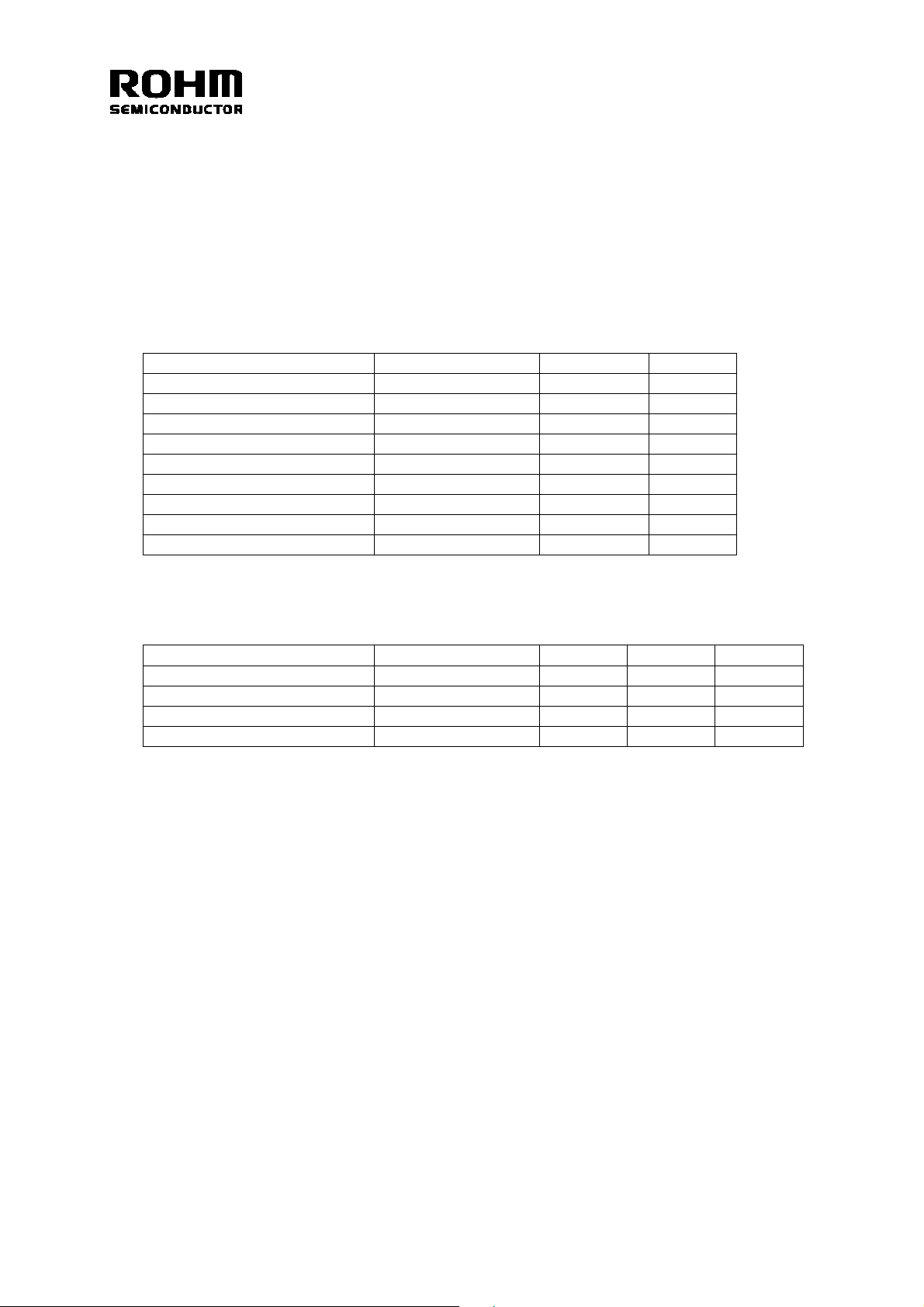
○ABSOLUTE MAXIMUM RATINGS(Ta=25℃)
Parameter Symbol Limit Unit
Input Voltage VCC 7
Enable Input Voltage VEN 7
Termination Input Voltage VTT_IN 7
VDDQ Reference Voltage VDDQ 7
*1*2
V
*1*2
V
*1*2
V
*1*2
V
Output Current ITT 1 A
Power Dissipation Pd 437.5 *3 mW
Operating Temperature Range Topr
Storage Temperature Range Tstg
Maximum Junction Temperature Tjmax +150
*1 Should not exceed Pd.
*2 Instantaneous surge voltage, back electromotive force and voltage under less than 10% duty cycle.
*3 Reduced by 3.5mW for each increase in Ta of 1℃ over 25℃(With no heat sink).
-40~+105 ℃
-55~+150 ℃
℃
○OPERATING CONDITIONS(Ta=25℃)
Parameter Symbol MIN MAX Unit
Input Voltage VCC 2.7 5.5 V
Termination Input Voltage VTT_IN 1.0 5.5 V
VDDQ Reference Voltage VDDQ 1.0 2.75 V
Enable Input Voltage VEN -0.3 5.5 V
★ This product is designed for protection against radioactive rays.
Status of this document
The Japanese version of this document is the official specification.
This translated version is intended only as a reference, to aid in understanding the official version.
If there are any differences between the original and translated versions of this document, the official Japanese language version takes priority.
REV. B
2/4
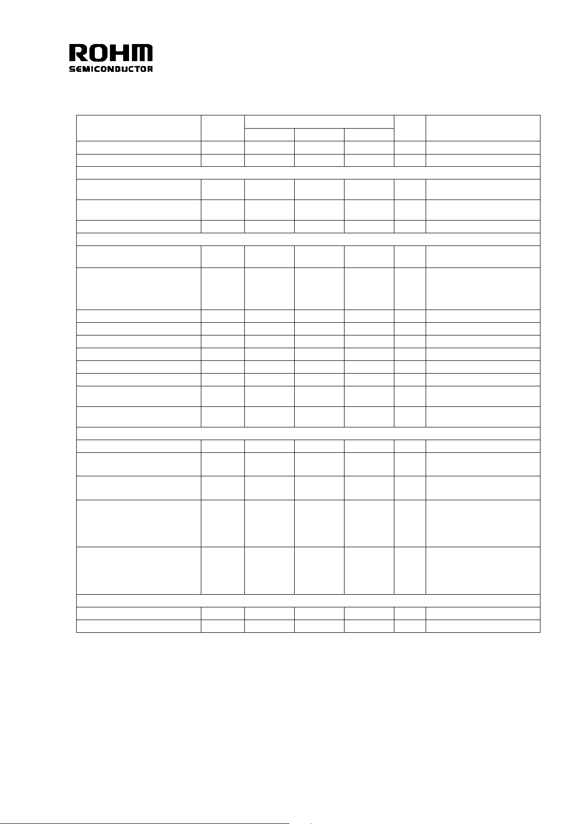
○ELECTRICAL CHARACTERISTICS
Parameter Symbol
(unless otherwise noted, Ta=25℃, VCC=3.3V, VEN=3V, VDDQ=1.8V, VTT_IN=1.8V)
Standard Value
MIN TYP MAX
Unit Condition
Standby Current IST - 0.5 1.0 mA VEN=0V
Bias Current ICC - 2 4 mA VEN=3V
[Enable]
High Level Enable Input
Voltage
Low Level Enable Input
Voltage
VENHIGH 2.3 - 5.5 V
VENLOW -0.3 - 0.8 V
Enable Pin Input Current IEN - 7 10 uA VEN=3V
[Termination]
Termination Output Voltage 1 VTT1 VREF-30m VREF VREF+30m V
ITT=-1.0A to 1.0A
Ta=0℃ to 105℃
VCC=5V, VDDQ=2.5V
Termination Output Voltage 2 VTT2 VREF-30m VREF VREF+30m V
VTT_IN=2.5V
ITT=-1.0A to 1.0A
Ta=0℃ to 105℃
Source Current ITT+ 1.0 - - A
Sink Current ITT- - - -1.0 A
Load Regulation
⊿VTT
- - 50 mV ITT=-1.0A to 1.0A
Line Regulation Reg.l - 20 40 mV
Upper Side ON Resistance 1 HRON1 - 0.45 0.9
Lower Side ON Resistance 1 LRON1 - 0.45 0.9
Upper Side ON Resistance 2 HRON2 - 0.4 0.8
Lower Side ON Resistance 2 LRON2 - 0.4 0.8
Ω
Ω
Vcc=5V, VDDQ=2.5V
Ω
VTT_IN=2.5V
Vcc=5V, VDDQ=2.5V
Ω
VTT_IN=2.5V
[Input of Reference Voltage]
Input Impedance ZVDDQ 70 100 130
Output Voltage 1 VREF1
Output Voltage 2 VREF2
1/2×VDDQ
-18m
1/2×VDDQ
-40m
1/2×VDDQ
1/2×VDDQ
1/2×VDDQ
+18m
1/2×VDDQ
+40m
kΩ
IREF=-5mA to 5mA
V
Ta=0℃ to 105℃
IREF=-10mA to 10mA
V
Ta=0℃ to 105℃
VCC=5V, VDDQ=2.5V
Output Voltage 3 VREF3
1/2×VDDQ
-25m
1/2×VDDQ
1/2×VDDQ
+25m
VTT_IN=2.5V
V
IREF=-5mA to 5mA
Ta=0℃ to 105℃
VCC=5V, VDDQ=2.5V
Output Voltage 4 VREF4
1/2×VDDQ
-40m
1/2×VDDQ
1/2×VDDQ
+40m
VTT_IN=2.5V
V
IREF=-10mA to 10mA
Ta=0℃ to 105℃
[UVLO]
UVLO OFF Voltage VUVLO 2.40 2.55 2.70 V VCC : sweep up
Hysteresis Voltage
⊿VUVLO
100 160 220 mV VCC : sweep down
REV. B

○PHYSICAL DIMENSION
3/4
D 3 5
3
8
1PIN MARK
Lot No.
(UNIT:mm)
MSOP8
○BLOCK DIAGRAM ○Pin number Pin name
VCC
C2
VDDQ
VTT_IN
C3
EN
Enable
Reference
Thermal
Protection
2
6
Block
EN
VCC
VDDQ
5 7
VCC
+
UVLO
TSD
1
GND
VCC
UVLO
SOFT
TSD
EN
UVLO
VCC
+
-
VCC
+
TSD
EN
UVLO
TSD
EN
UVLO
VTT_IN
VTT
8
3
VTTS
VREF
4
Pin
number
Pin name
1 GND
2 EN
VTT
C4
3 VTTS
4 VREF
5 VDDQ
6 VCC
7 VTT_IN
C1
½×
VDDQ
8 VTT
REV. B
4/4
○NOTES FOR USE
(1) Absolute maximum range
Although the quality of this product is rigorously controlled, and circuit operation is guaranteed within the operation ambient
temperature range, the device may be destroyed when applied voltage or operating temperature exc eeds its absolute maximum
rating. Because the failure mode (such as short mode or open mode) cannot be identified in this instance, it is important to take
physical safety measures such as fusing if a specific mode in excess of absolute rating limits is considered for implementation.
(2) Ground potential
Make sure the potential for the GND pin is always kept lower than the potentials of all other pins, regardless of the operating
mode, including transient conditions.
(3) Thermal Design
Provide sufficient margin in the thermal design to account for the allowable power dissipation (Pd) expected in actual use.
(4) Using in the strong electromagnetic field
Use in strong electromagnetic fields may cause malfunctions.
(5) ASO
Be sure that the output transistor for this IC does not exceed the absolute maximum ratings or ASO value.
(6) Thermal shutdown circuit
The IC is provided with a built-in thermal shutdown (TSD) circuit. When chip temperature reaches the threshold temperature
shown below, output goes to a cut-off (open) state. Note that the TSD circuit is designed exclusively to shut down the IC in
abnormal thermal conditions. It is not intended to protect the IC per se or guarantee performance when extreme heat occurs.
Therefore, the TSD circuit should not be employed with the expectation of continued use or subsequent operation once TSD is
operated.
(7) GND pattern
When both a small-signal GND and high current GND are present, single-point grounding (at the set standard point) is
recommended, in order to separate the small-signal and high current patterns, and to be sure the voltage change stemming from
the wiring resistance and high current does not cause any voltage change in the small-signal GND. In the same way, care must
be taken to avoid wiring pattern fluctuations in any connected external component GND.
(8) Output Capacitor (C1)
Mount an output capacitor between VREF and GND for stability purposes. The VREF output capacitor is for the open loop gain
phase compensation. If the capacitor value is not large enough, the output voltage may oscillate. A ceramic 1.0 - 10uF capacitor
with minimal susceptibility to temperature is recommended. However, this stability depends on the characteristics of temperature
and load. Please confirm operation across a variety of temperature and load conditions.
(9) Output Capacitor (C4)
Mount an output capacitor between VTT and GND for stability purposes. The output capacitor is for the open loop gain phase
compensation and reduces the output voltage load regulation. If the capacitor value is not large enough, the output voltage may
oscillate. And if the equivalent series resistance (ESR) is too large, the output voltage rise/drop increases during a sudden load
change. A 47 - 220uF polymer capacitor is recommended. However, the stability depends on the characteristics of temperature
and load conditions. And if a small ESR capacitor such as a ceramic capacitor is utilized, the output voltage may oscillate due to
lack of phase margin. In this case, measures can be taken by adding a resistor in series with this capacitor. Please confirm
operation across a variety of temperature and load conditions.
(10) Input Capacitor (C2, C3)
The input capacitor reduces the output impedence of the voltage supply source connected in the VCC and VTT_IN. If the output
impedence of this power supply increases, the input voltage (VCC,VTT_IN) may become unstable. This may result in the output
voltage oscillation or lowering ripple rejection. A low ESR 1uF capacitor in VCC and 10uF capacitor in VTT_IN with minimal
susceptibility to temperature are preferable, but stability depends on power supply characteristics and the substrate wiring
pattern (a parasitic capacitance and impedance). Please confirm operation across a variety of temperature and load conditions.
(11) Input (VCC, VDDQ, VTT_IN, EN)
The VCC, VDDQ, VTT_IN, and EN are isolated. The UVLO function is integrated to protect faulty operation due to low voltage
levels of VCC. VTT output voltage starts up when VCC reaches the UVLO threshold level and EN reaches the threshold level
respectively regardless of the start up order in those inputs. And also VREF output voltage starts up when VCC reaches the
UVLO threshold level. When the VDDQ and VTT_IN has the same voltage and are supposed to connect each other, VDDQ pin
voltage may change due to the voltage drop on the VTT_IN and VDDQ common wiring caused by VTT_IN input cu rrent change.
This may result in the voltage change of the VTT output. Avoid drawing wiring pattern of VDDQ and VTT_IN so that they do not
have common wiring. If the common wiring is inevitable due to limited PCB area, it is recommended that CR filter be added
between VTT_IN and VDDQ.
(12) VTTS
VTTS is to improve load regulation of VTT output. For precise load regulation, VTTS is connected close by VTT to avoid
common impedance.
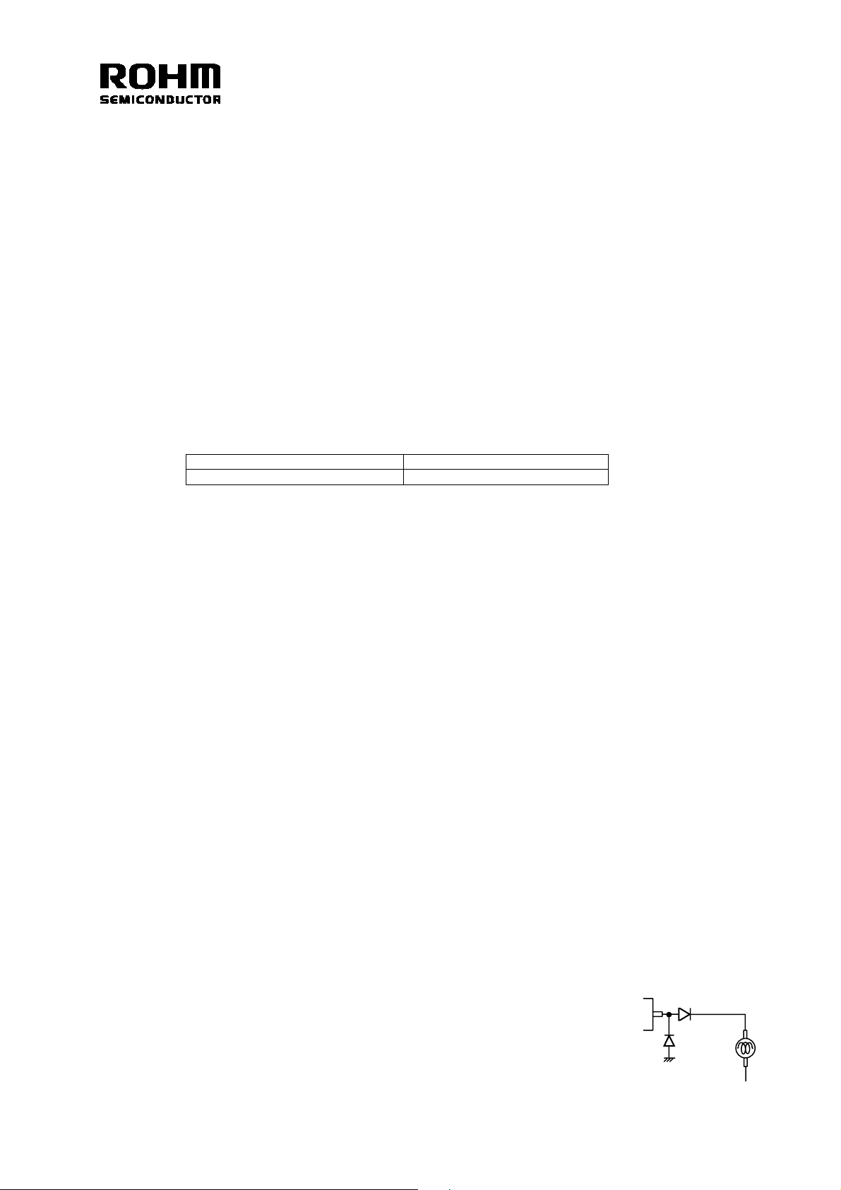
(13) Please add a protection diode when a large inductance component is
connected to the output terminal, and reverse-polarity power is possible at
startup or in output OFF condition.
TSD ON temperature [℃] (typ.) Hysteresis temperature [℃] (typ.)
175 15
(Example)
OUTPUT PIN
REV. B

Appendix
No copying or reproduction of this document, in part or in whole, is permitted without the consent of ROHM
CO.,LTD.
The content specified herein is subject to change for improvement without notice.
The content specified herein is for the purpose of introducing ROHM's products (hereinafter "Products"). If you
wish to use any such Product, please be sure to refer to the specifications, which can be obtained from ROHM
upon request.
Examples of application circuits, circuit constants and any other information contained herein illustrate the
standard usage and operations of the Products. The peripheral conditions must be taken into account
when designing circuits for mass production.
Great care was taken in ensuring the accuracy of the information specified in this document. However, should
you incur any damage arising from any inaccuracy or misprint of such information, ROHM shall bear no re-
sponsibility for such damage.
The technical information specified herein is intended only to show the typical functions of and examples
of application circuits for the Products. ROHM does not grant you, explicitly or implicitly, any license to
use or exercise intellectual property or other rights held by ROHM and other parties. ROHM shall bear no re-
sponsibility whatsoever for any dispute arising from the use of such technical information.
The Products specified in this document are intended to be used with general-use electronic equipment
or devices (such as audio visual equipment, office-automation equipment, communication devices, elec-
tronic appliances and amusement devices).
The Products are not designed to be radiation tolerant.
While ROHM always makes efforts to enhance the quality and reliability of its Products, a Product may fail or
malfunction for a variety of reasons.
Please be sure to implement in your equipment using the Products safety measures to guard against the
possibility of physical injury, fire or any other damage caused in the event of the failure of any Product, such as
derating, redundancy, fire control and fail-safe designs. ROHM shall bear no responsibility whatsoever for your
use of any Product outside of the prescribed scope or not in accordance with the instruction manual.
The Products are not designed or manufactured to be used with any equipment, device or system
which requires an extremely high level of reliability the failure or malfunction of which may result in a direct
threat to human life or create a risk of human injury (such as a medical instrument, transportation equipment,
aerospace machinery, nuclear-reactor controller, fuel-controller or other safety device). ROHM shall bear
no responsibility in any way for use of any of the Products for the above special purposes. If a Product is intend-
ed to be used for any such special purpose, please contact a ROHM sales representative before purchasing.
If you intend to export or ship overseas any Product or technology specified herein that may be controlled under
the Foreign Exchange and the Foreign Trade Law, you will be required to obtain a license or permit under the Law.
Notes
Thank you for your accessing to ROHM product informations.
More detail product informations and catalogs are available, please contact your nearest sales office.
ROHM Customer Support System
www.rohm.com
Copyright © 2009 ROHM CO.,LTD.
21 Saiin Mizosaki-cho, Ukyo-ku, Kyoto 615-8585, Japan
THE AMERICAS / EUROPE / ASIA / JAPAN
Contact us : webmaster@ rohm.co. jp
TEL : +81-75-311-2121
FAX : +81-75-315-0172
Appendix-Rev4.0
 Loading...