

Page 1
TECHNICAL NOTE
High-performance Regulator IC Series for PCs
Termination Regulators
for DDR-SDRAMs
BD3533F/FVM/EKN(1A),BD3531F(1.5A),BD3532F/EFV/KN(3A)
Description
BD3533/31/32 is a termination regulator compatible with JEDEC DDR-SDRAM, which functions as a linear po wer supply
incorporating an N-channel MOSFET and provides a sink/source current capability up to 1A, 1.5A, and 3A respectively. A
built-in high-speed OP-AMP specially designed offers an excellent transient response. Requires 3.3 volts or 5.0 volts as a
bias power supply to drive the N-channel MOSFET. Has an independent reference voltage input pin (VDDQ) and an
independent feedback pin (VTTS) to maintain the accuracy in voltage required by JEDEC, and offers an excellent o utput
voltage accuracy and load regulation. Also has a reference power supply output pin (VREF) for DDR-SDRAM or a
memory controller. When EN pin turns to “Low”, VTT output becomes “Hi-Z” while VREF output is kept unchanged,
compatible with “Self Refresh” state of DDR-SDRAM.
Features
1) Incorporates a push-pull power supply for termination (VTT)
2) Incorporates a reference voltage circuit (VREF)
3) Incorporates an enabler
4) Incorporates an undervoltage lockout (UVLO)
5). Employs SOP8 package
6) Employs MSOP8 package
7) Employs HQFN20V package
8) Employs HTSSOP-B20 package
9) Employs VQFN28V package
10) Incorporates a thermal shutdown protector (TSD)
11) Operates with input voltage from 2.7 to 5.5 volts
12) Compatible with Dual Channel (DDR-II)
Use
Power supply for DDR I/II - SDRAM
●Line up
Parameter BD3533F/FVM/EKN BD3531F BD3532F/EFV/KN
Output Current ±1.0A ±1.5A ±3A
Vcc Range 2.7V~5.5V 4.5V~5.5V 4.3~5.5V
Soft Start Function ○ × ○
Temperature -20~100℃ -10~100℃ -40~100℃
Package SOP8/MSOP8/HQFN20V SOP8 SOP8/HTSSOP-B20/VQFN28
Oct. 2008
Page 2
●ABSOLUTE MAXIMUM RATINGS
◎BD3533F/FVM/EKN
Parameter Symbol
Input Voltage VCC 7
Enable Input Voltage VEN 7
Termination Input Voltage VTT_IN 7
VDDQ Reference Voltage VDDQ 7
Output Current ITT 3 1 3 A
Power Dissipation1 Pd1 560 *3 437.5
Power Dissipation2 Pd2 690 *4
Power Dissipation3 Pd3
Power Dissipation4 Pd4
Operating Temperature Range Topr -20~+100 -20~+100 -20~+100 ℃
Storage Temperature Range Tstg -55~+150 -55~+150 -55~+150 ℃
Maximum Junction Temperature Tjmax +150 +150 +150 ℃
*1 Should not exceed Pd.
*2 Instantaneous surge voltage, back electromotive force and voltage under less than 10% duty cycle.
*3 Reduced by 4.48mW for each increase in Ta of 1℃ over 25℃(With no heat sink).
*4 Reduced by 5.52mW for each increase in Ta of 1℃ over 25℃(When mounted on a board 70mm×70mm×1.6mm Glass-epoxyPCB).
*5 Reduced by 3.5mW for each increase in Ta of 1℃ over 25℃(With no heat sink).
*6 Ta≧25℃(no heat sink)4mW/℃ increase.
*7 Ta≧25℃(when mounted on 70mm x 70mm x 1.6mm Glass-epoxy PCB which does not have copper on the back side).
*8 Ta≧25℃(when mounted on 70mm x 70mm x 1.6mm Glass-epoxy PCB which has 1 layer ( 60mm x 60mm ) of copper on the back side)14mW/℃ increase.
*9 Ta≧25℃(When mounted on board 70mm x 70mm x 1.6mm Glass-epoxy PCB which has 2 layers ( 60mm x 60mm ) of copper on the back side )16mW/℃
increase.
◎BD3531F
Parameter Symbol Limit Unit
Input Voltage VCC 7 *1 V
EN Input Voltage VEN 7 *1 V
Termination Input Voltage VTT_IN 7 *1 V
VDDQ Reference Voltage VDDQ 7 *1 V
Output Current ITT 3 A
Power Dissipation1 Pd1 560 *2 mW
Power Dissipation2 Pd2 690 *3 mW
Operating Temperature Range Topr
Storage Temperature Range Tstg
Maximum Junction Temperature Tjmax +150 ℃
*1 Should not exceed Pd.
*2 Reduced by 4.48mW for each increase in Ta of 1℃ over 25℃(With no heat sink).
*3 Reduced by 5.52mW for each increase in Ta of 1℃ over 25℃(When mounted on a board 70mm×70mm×1.6mm Glass-epoxyPCB).
◎BD3532F/EFV/KN
Parameter Symbol
Input Voltage VCC 7 *1 7 *1 7 *1 V
Enable Input Voltage VEN 7 *1 7 *1 7 *1 V
Termination Input Voltage VTT_IN 7 *1 7 *1 7 *1 V
VDDQ Reference Voltage VDDQ 7 *1 7 *1 7 *1 V
Output Current ITT 3 3 3 A
Power Dissipation1 Pd1 560 *2 - 460 *5 mW
Power Dissipation2 Pd2 690 *3
Operating Temperature Range Topr -40~+100 -40~+100 -40~+100 ℃
Storage Temperature Range Tstg -55~+150 -55~+150 -55~+150 ℃
Maximum Junction Temperature Tjmax +150 +150 +150 ℃
*1 Should not exceed Pd.
*2 Reduced by 4.48mW for each increase in Ta of 1℃ over 25℃(With no heat sink).
*3 Reduced by 5.52mW for each increase in Ta of 1℃ over 25℃(When mounted on a board 70mm×70mm×1.6mm Glass-epoxyPCB).
*4 Reduced by 8.0mW for each increase in Ta of 1℃ over 25℃(When mounted on a board 70mm×70mm×1.6mm Glass-epoxyPCB).
*5 Reduced by 3.68mW for each increase in Ta of 1℃ over 25℃(With no heat sink).
*6 Reduced by 5.80mW for each increase in Ta of 1℃ over 25℃(When mounted on a board 70mm×70mm×1.6mm Glass-epoxyPCB).
BD3533F BD3533FVM
*1*2
7
*1*2
7
*1*2
7
*1*2
7
*1*2
7
*1*2
7
*1*2
7
*1*2
7
*5
500
-
- -
- -
-10~
-55~
BD3532F BD3532EFV
℃
℃
1000 *
BD3532KN Unit
4
2/16
BD3533EKN Unit
*1*2
V
*1*2
V
*1*2
V
*1*2
V
*6
mW
750 *7 mW
1750 *8 mW
2000 *9 mW
6
725 *
mW
Page 3
●RECOMMENDED OPERATING CONDITIONS
◎BD3533F/FVM/EKN(Ta=25℃)
Parameter Symbol MIN MAX Unit
Input Voltage VCC 2.7 5.5 V
Termination Input Voltage VTT_IN 1.0 5.5 V
VDDQ Reference Voltage VDDQ 1.0 2.75 V
Enable Input Voltage VEN -0.3 5.5 V
◎BD3531F(Ta=25℃)
Parameter Symbol MIN MAX Unit
Input Voltage VCC 4.5 5.5 V
Termination Input Voltage VTT_IN 1.0 5.5 V
EN Input Voltage VEN -0.3 5.5 V
◎BD3532F/EFV/KN(Ta=25℃)
Parameter Symbol MIN MAX Unit
Input Voltage VCC 4.3 5.5 V
Termination Input Voltage VTT_IN 1.0 5.5 V
EN Input Voltage VEN -0.3 5.5 V
★ No radiation-resistant design is adopted for the present product.
●ELECTRICAL CHARACTERISTICS
◎BD3533F/FVM/EKN
ELECTRICAL CHARACTERISTICS(unless otherwise noted, Ta=25℃ VCC=3.3V VEN=3V VDDQ=1.8V VTT_IN=1.8V)
Parameter Symbol
Standard Value
MIN TYP MAX
Unit Condition
Standby Current IST - 0.8 1.6 mA VEN=0V
Bias Current ICC - 2 4 mA VEN=3V
[Enable]
High Level Enable Input Voltage VENHIGH 2.3 - 5.5 V
Low Level Enable Input Voltage VENLOW -0.3 - 0.8 V
Enable Pin Input Current IEN - 7 10 uA VEN=3V
[Termination]
Termination Output Voltage 1 VTT1
VREF
-30m
VREF
VREF
+30m
ITT=-1.0A to 1.0A
V
Ta =0 ℃ to 100℃
VCC=5V, VDDQ=2.5V
Termination Output Voltage 2 VTT2
VREF
-30m
VREF
VREF
+30m
VTT_IN=2.5V
V
ITT=-1.0A to 1.0A
Ta =0 ℃ to 100℃
Source Current ITT+ 1.0 - - A
Sink Current ITT- - - -1.0 A
Load Regulation ⊿VTT - - 50 mV ITT=-1.0A to 1.0A
Line Regulation Reg.l - 20 40 mV
Upper Side ON Resistance 1 HRON1 - 0.45 0.9 Ω
Lower Side ON Resistance 1 LRON1 - 0.45 0.9 Ω
Upper Side ON Resistance 2 HRON2 - 0.4 0.8 Ω
Lower Side ON Resistance 2 LRON2 - 0.4 0.8 Ω
VCC=5V, VDDQ=2.5V
VTT_IN=2.5V
VCC=5V, VDDQ=2.5V
VTT_IN=2.5V
*7 Design Guarantee
*7
*7
3/16
Page 4
●ELECTRICAL CHARACTERISTICS
◎BD3533F/FVM/EKN
ELECTRICAL CHARACTERISTICS(unless otherwise noted, Ta=25℃ VCC=3.3V VEN=3V VDDQ=1.8V VTT_IN=1.8V)
Parameter Symbol
MIN TYP MAX
Standard Value
Unit Condition
[Input of Reference Voltage]
Input Impedance ZVDDQ 70 100 130 kΩ
Output Voltage1 VREF1
Output Voltage2 VREF2
Output Voltage3 VREF3
1/2×VDDQ
-18m
1/2×VDDQ
-40m
1/2×VDDQ
-25m
1/2×VDDQ
1/2×VDDQ
1/2×VDDQ
1/2×VDDQ
+18m
1/2×VDDQ
+40m
1/2×VDDQ
+25m
IREF=-5mA to 5mA
V
Ta =0 ℃ to 100℃
IREF=-10mA to 10mA
V
Ta =0 ℃ to 100℃*7
VCC=5V, VDDQ=VTT_IN=2.5V
IREF=-5mA to 5mA
V
Ta =0 ℃ to 100℃
*7
*7
VCC=5V, VDDQ=VTT_IN=2.5V
IREF=-10mA to 10mA
V
Ta =0 ℃ to 100℃
*7
Output Voltage4 VREF4
1/2×VDDQ
-40m
1/2×VDDQ
1/2×VDDQ
+40m
[Reference voltage]
Source Current IREF+ 20 - - mA
Sink Current IREF- - - -20 mA
[UVLO]
UVLO OFF Voltage VUVLO 2.40 2.55 2.70 V VCC : sweep up
Hysteresis Voltage ⊿VUVLO 100 160 220 mV VCC : sweep down
*7 Design Guarantee
◎BD3531F
ELECTRICAL CHARACTERISTICS(unless otherwise noted, Ta=25℃ VCC=5V VEN=3V VDDQ=2.5V VTT_IN=2.5V)
Parameter Symbol
Standard Value
MIN TYP MAX
Unit Condition
Standby Current IST - 0.8 1.6 mA VEN=0V
Bias Current ICC - 2 4 mA
[Enable]
Hi Level Enable Input Voltage VENHI 2 - 5.5 V
Low Level Enable Input Voltage VENLOW -0.3 - 0.8 V
Enable Pin Input Current IEN - 7 10 uA VEN=3V
[Termination]
Termination Output Voltage VTT
VREF
-30mV
VREF
VREF
+30mV
Io=-1.5A to 1.5A
V
Ta =0 ℃ to 100℃ *
8
Source Current ITT+ 1.5 - - A
Sink Current ITT- - - -1.5 A
Load Regulation ⊿VTT - - 40 mV Io=-1.5A to 1.5A
Line Regulation Reg.l - 20 40 mV VCC=4.5V to 5.5V
Upper Side ON Resistance HRON - 0.4 0.8 Ω
Lower Side ON Resistance LRON - 0.4 0.8 Ω
[Input of Reference Voltage]
Input Impedance ZVDDQ - 100 - kΩ
[Reference voltage]
Output Voltage1 VREF1 1/2×VDDQ-30m 1/2×VDDQ 1/2×VDDQ+30m V IREF=0mA
Output Voltage2 VREF2
1/2×VDDQ
-40m
1/2×VDDQ
1/2×VDDQ
+40m
IREF=-10mA to 10mA
V
Ta =0 ℃ to 100℃ *8
Source Current IREF+ 10 20 - mA
Sink Current IREF- - -20 -10 mA
[UVLO]
UVLO OFF Voltage VUVLO 4.2 4.35 4.5 V VCC : Sweep up
Hysteresis Voltage ⊿VUVLO 100 160 220 mV VCC : Sweep down
*8 Design Guarantee
4/16
Page 5

◎BD3532F/EFV/KN
ELECTRICAL CHARACTERISTICS(unless otherwise noted, Ta=25℃ VCC=5V VEN=3V VDDQ=2.5V VTT_IN=2.5V)
Parameter Symbol
MIN TYP MAX
Standard Value
Unit Condition
Standby Current IST - 0.8 1.6 mA VEN=0V
Bias Current ICC - 2 4 mA
[Enable]
Hi Level Enable Input
Voltage
Low Level Enable Input
Voltage
VENHI 2.3 - 5.5 V
VENLOW -0.3 - 0.8 V
VCC=4.3V to 5.5V
Ta =0 ℃ to 100℃ *
VCC=4.3V to 5.5V
Ta =0 ℃ to 100℃ *
9
9
Enable Pin Input Current IEN - 7 10 uA VEN=3V
[Termination]
Termination Output Voltage VTT
VREF
-30mV
VREF
VREF
+30mV
Io=-3A to 3A
V
Ta =0 ℃ to 100℃ *9
Source Current ITT+ 3 - - A
Sink Current ITT- - - -3 A
Load Regulation ⊿VTT - - 40 mV Io=-3A to 3A
Line Regulation Reg.l - 20 40 mV VCC=4.3V to 5.5V
Upper Side ON Resistance HRON - 0.2 0.4 Ω
Lower Side ON Resistance LRON - 0.2 0.4 Ω
[Input of Reference Voltage]
Input Impedance ZVDDQ 70 100 130 kΩ
Output Voltage1 VREF1
Output Voltage2 VREF2
Output Voltage1’ VREF1’
Output Voltage2’ VREF2’
1/2×VDDQ
-30mV
1/2×VDDQ
-40mV
1/2×VDDQ
-30mV
1/2×VDDQ
-40mV
1/2×VDDQ
1/2×VDDQ
1/2×VDDQ
1/2×VDDQ
1/2×VDDQ
+30mV
1/2×VDDQ
+40mV
1/2×VDDQ
+30mV
1/2×VDDQ
+40mV
V IREF=0mA
IREF=-10mA to 10mA
V
Ta =0 ℃ to 100℃ *9
VDDQ=VTT_IN1=VTT_IN2=1.8V
V
IREF=0mA
VDDQ=VTT_IN1=VTT_IN2=1.8V
V
IREF=-10mA to 10mA
Ta =0 ℃ to 100℃ *
9
Source Current1 IREF1+ 20 - - mA
Sink Current1 IREF1- - - -20 mA
Source Current2 IREF2+ 20 - - mA VDDQ=VTT_IN1=VTT_IN2=1.8V
Sink Current2 IREF2- - - -20 mA VDDQ=VTT_IN1=VTT_IN2=1.8V
[UVLO]
UVLO OFF Voltage VUVLO 4.0 4.15 4.3 V VCC : sweep up
Hysteresis Voltage ⊿VUVLO 100 160 220 mV VCC : sweep down
*9 Design Guarantee
5/16
Page 6
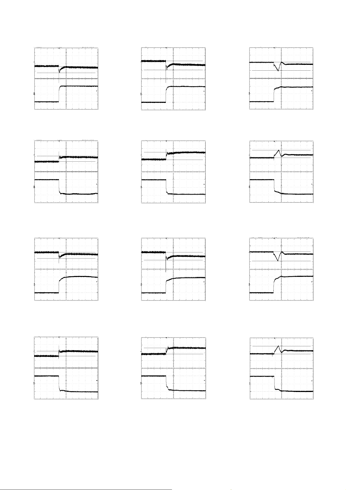
●Reference Data
(
VTT(10mV/Div)
VTT(10mV/Div)
VTT(20mV/Div)
ITT(1A/Div)
10μsec/Div 10μsec/Div 10μsec/Div
ITT(1A/Div)
ITT(1A/Div)
Fig.1 DDRⅠ(-1A→1A) BD3531 Fig.3 DDRⅠ(-1A→1A) BD3533
Fig.2 DDRⅠ(-1A→1A) BD3532
VTT
10mV/Div)
VTT(10mV/Div)
VTT(20mV/Div)
ITT(1A/Div)
ITT(1A/Div)
ITT(1A/Div)
10μsec/Div 10μsec/Div 10μsec/Div
Fig.4 DDRⅠ(1A→-1A) BD3531 Fig.5 DDRⅠ(1A→-1A) BD3532 Fig.6 DDRⅠ(1A→-1A) BD3533
VTT(10mV/Div)
VTT(10mV/Div)
VTT(20mV/Div)
Fig.7 DDRⅡ(-1A→1A) BD3531 Fig.8 DDRⅡ(-1A→1A) BD3532 Fig.9 DDRⅡ(-1A→1A) BD3533
ITT(1A/Div)
10μsec/Div 10μsec/Div 10μsec/Div
ITT(1A/Div)
ITT(1A/Div)
VTT(10mV/Div)
VTT(10mV/Div)
VTT(20mV/Div)
ITT(1A/Div)
10μsec/Div 10μsec/Div 10μsec/Div
ITT(1A/Div)
ITT(1A/Div)
Fig.10 DDRⅡ(1A→-1A) BD3531 Fig.11 DDRⅡ(1A→-1A) BD3532 Fig.12 DDRⅡ(1A→-1A) BD3533
6/16
Page 7

(mA)
(
)
1.252
1.251
VREF(V)
1.249
1.25
VREF(V)
0.902
0.901
0.9
0.899
0.898
1.248
-10 -5 0 5 10
Fig.13 IREF-VREF (DDR-Ⅰ) Fig.14 IREF-VREF (DDR-Ⅱ) Fig.15 ITT-VTT (DDR-Ⅰ)
IREF (mA)
0.897
-10 -5 0 5 10
IREF
1.258
1.256
1.254
1.252
1.250
VTT(V)
1.248
1.246
1.244
-2 -1 0 1 2
ITT(A)
0.91
0.912
0.91
0.910
0.90
0.908
0.90
0.906
V
0.90
0.904
VTT
VTT(V)
0.90
0.902
0.90
0.900
0.89
0.898
0.896
0.89
-2 -1 0 1 2
Fig.16 ITT-VTT (DDR-Ⅱ)
ITT(A)
VCC
EN
VDDQ
VTT IN
VTT
Fig.17 Input Sequence 1
VCC
EN
VDDQ
VTT IN
VTT
Fig.18 Input Sequence 2
VCC
EN
VTT_IN
VTT
VDDQ
VTT IN
VTT
VREF
ITT_IN
(1A/div)
Fig.19 Input Sequence 3
Fig.20 Start up Wave Form
7/16
Page 8

●BLOCK DIAGRAM
◎BD3533F/FVM/EKN
Enable
◎BD3531F
Enable
◎BD3532F/FVM/EKN
Enable
EN
EN
EN
VCC
VCC
Reference
Block
Thermal
Protection
EN
VCC
VCC
Reference
Block
Thermal
Protection
VCC
VCC
Reference
Block
Thermal
Protection
EN
VCC
VCC
TSD
EN
UVLO
TSD
EN
UVLO
TSD
EN
UVLO
TSD
EN
UVLO
TSD
EN
UVLO
TSD
EN
UVLO
VTT_IN
VTT_IN
VTT_IN
VTT_IN
VTT
VTT
VTTS
VREF
VREFS
VTT_IN
VTT_IN
VTT
VTTS
VREF
VTT
VTTS
VREF
VTT
½×
VDDQ
VTT
½×
VDDQ
VTT
½×
VDDQ
VDDQ
SOFT
TSD
EN
UVLO
UVLO
VTT_IN
VCC
SOFT
VDDQ
VCC VCC VCC
UVLO
UVLO
TSD
DGND PGND
VDDQ
VDDQ
VCC VCC
UVLO
VDDQ
VDDQ
VCC VCC
UVLO
TSD
TSD
VCC
GND
GND
VCC
50kΩ
UVLO
50kΩ
50kΩ
UVLO
50kΩ
8/16
Page 9

◎BD3533F/BD3533FVM/BD3531F/BD3532F
●PIN CONFIGRATION ●PIN FUNCTION
PIN No.
GND
1
EN
2
VTTS
3
4 5
VREF
8
7
6
VTT
VTT_IN
VCC
VDDQ
1 GND GND Pin
2 EN Enable Input Pin
3 VTTS Detector Pin for Termination Voltage
4 VREF Reference Voltage Output Pin
5 VDDQ Reference Voltage Input Pin
6 VCC VCC Pin
7 VTT_IN Termination Input Pin
8 VTT Termination Output Pin
◎BD3532KN
●PIN CONFIGRATION ●PIN FUNCTION
PIN No. PIN NAME PIN FUNCTION
1 PGND1 Power Ground Pin 1
2 PGND2 Power Ground Pin 2
3 SGND Ground Pin for Reference Voltage
4 EN Enable Input Pin
5 N.C. Non Connection
6 VTTS Detector Pin for Termination Voltage
7 N.C. Non Connection
8 N.C. Non Connection
9 N.C. Non Connection
10 VREF Reference Voltage Output Pin
11 VREFS Detector Pin for Reference Voltage
12 VDDQ Reference Voltage Input Pin
13 N.C. Non Connection
14 N.C. Non Connection
15 N.C. Non Connection
16 VCC VCC Pin
17 N.C. Non Connection
18 N.C. Non Connection
19 VTT_IN1 Termination Input Pin 1
20 VTT_IN2 Termination Input Pin 2
21 N.C. Non Connection
22 N.C. Non Connection
23 N.C. Non Connection
24 VTT1 Termination Output Pin 1
25 VTT2 Termination Output Pin 2
26 N.C. Non Connection
27 N.C. Non Connection
28 N.C. Non Connection
NC
NC
VTT1
VTT2
NC
NC
NC
VTT_IN2
NC
PGND1
VTT_IN1
SGND
PGND2
EN
NC
VCC
NC
NC
NC
VDDQ
VREFS
VREF
NC
NC
NC
VTTS
◎BD3533EKN
●PIN CONFIGRATION ●PIN FUNCTION
PIN No.
1 DGND Digital Ground Pin
2 EN Enable Input Pin
3 NC Non Connection
4 VTTS Detector Pin for Termination Voltage
5 VREF Reference Voltage Output Pin
6 VREFS Detector Pin for Reference Voltage
7 NC Non Connection
8 NC Non Connection
9 NC Non Connection
10 VDDQ Reference Voltage Input Pin
11 NC Non Connection
12 VCC VCC Pin
13 VTT_IN
14 VTT_IN
15 VTT Termination Output Pin
16 VTT Termination Output Pin
17 NC Non Connection
18 NC Non Connection
19 NC Non Connection
20 PGND Power Ground Pin
VTT
NC
NC
NC
PGND
VTT VTT_IN VTT_IN
15 14 13 12 11
16
17
18
19
20
1 2 3 4 5
DGND
VCC
VREF VTTS NC EN
NC
10
9
8
7
6
VDDQ
NC
NC
NC
VREFS
PIN NAME PIN FUNCTION
PIN NAME PIN FUNCTION
Termination Input Pin
Termination Input Pin
9/16
Page 10

◎BD3532EFV
A
●PIN CONFIGRATION ●PIN FUNCTION
VTT1
VTT2
PGND1
PGND2
SGND
EN
VTTS
NC
VREF
VREFS
GND
NC
NC
VTT_IN
VTT_IN
NC
VCC
NC
VDDQ
NC
PIN No.
1 VTT1 Termination Output Pin 1
2 VTT2 Termination Output Pin 2
3 PGND1 Power Ground Pin 1
4 PGND2 Power Ground Pin 2
5 SGND Ground Pin for Reference Voltage
6 EN Enable Input Pin
7 VTTS Detector Pin for Termination Voltage
8 N.C. Non Connection
9 VREF Reference Voltage Output Pin
10 VREFS Detector Pin for Reference Voltage
11 N.C. Non Connection
12 VDDQ Reference Voltage Input Pin
13 N.C. Non Connection
14 VCC VCC Pin
15 N.C. Non Connection
16 VTT_IN1 Termination Input Pin 1
17 VTT_IN2 Termination Input Pin 2
18 N.C. Non Connection
19 N.C. Non Connection
20 AGND Ground Pin for Analog Ground
- FIN Substrate (Connected to AGND)
PIN NAME PIN FUNCTION
●Description of operations
・VCC
In BD3533/31/32, an independent power input pin is provided for an internal circuit operation of the IC. This is used to drive
the amplifier circuit of the IC, and its maximum current rating is 4 mA. The power supply voltage is 3.3 to 5.5 volts (BD3533)
or 5 volts (BD3531/32). It is recommended to connect a bypass capacitor of 1 μF or so to VCC.
・VDDQ
Reference input pin for the output voltage, that may be used to satisfy the JEDEC requirement for DDR-SDRAM (VTT =
1/2VDDQ) by dividing the voltage inside the IC with two 50 kΩ voltage-divider resistors
For BD3533, care must be taken to an input noise to VDDQ pin because this IC also cuts such noise input into half and
provides it with the voltage output divided in half. Such noise may be reduced with an RC filter consisting of such resistance
and capacitance (220 Ω and 2.2 μF, for instance) that may not give significant effect to voltage dividing inside the IC.
・VTT_IN
VTT_IN is a power supply input pin for VTT output. Voltage in the range between 1.0 and 5.5 volts may be supplied to this
VTT_IN terminal, but care must be taken to the current limitation due to on-resistance of the IC and the change in allowable
loss due to input/output voltage difference.
Generally, the following voltages are supplied:
・ DDR I VTT_IN=2.5V
・ DDRII VTT_IN=1.8V
Higher impedance of the voltage input at VTT_IN may result in oscillation or degradation in ripple rejection, which must be
noted. To VTT_IN terminal, it is recommended to use a 10 μF capacitor characterized with less change in capacitance. But
it may depend on the characteristics of the power supply input and the impedance of the pc board wiring, which must be
carefully checked before use.
・VREF
In BD3533/31/32, a reference voltage output pin independent from VTT output is given to provide a reference input for a
memory controller and a DRAM. Even if EN pin turns to “Low” level, VREF output is kept unchanged, compatible with “Self
Refresh” state of DRAM. The maximum current capability of VREF is 20 mA, and a suitable capacitor is needed to stabilize
the output voltage. It is recommended to use a combination of a 1.0 to 2.2 μF ceramic capacitor characterized with less
change in capacitance and a 0.5 to 2.2 Ω phase compensator resistor, or a 10μF ceramic or tantalum capacitor instead. For
an application where VREF current is low, a capacitor of lower capacitance may be used. If VREF current is 1 mA or less, it
is possible to secure a phase margin with a ceramic capacitor of 1 μF more or less.
・VTTS
An independent pin provided to improve load regulation of VTT output. In case that longer wiring is needed to the load at
VTT output, connecting VTTS from the load side may improve the load regulation.
10/16
Page 11

・VTT
A DDR memory termination output pin. BD3533/31/32 has a sink/source current capability of ±1.0A/±1.5A/±3.0A
respectively. The output voltage tracks the voltage divided in half at VDDQ pin. VTT output is turned to OFF when VCC
UVLO or thermal shutdown protector is activated with EN pin level turned to “Low”. Do not fail to connect a capacitor to
VTT output pin for a loop gain phase compensation and a reduction in output voltage variation in the event of sudden change
in load. Insufficient capacitance may cause an oscillation. High ESR (Equivalent Series Resistance) of the capacitor may
result in increase in output voltage variation in the event of sudden change in load. It is recommended to use a 220 μF
functional polymer capacitor (OS-CON, POS-CAP, NEO-CAP), though it depends on ambient temperature and other
conditions. A low ESR ceramic capacitor may reduce a loop gain phase margin and may cause an oscillation, which may
be improved by connecting a resistor in series with the capacitor.
・EN
With an input of 2.3 volts or higher, the level at EN pin turns to “High” to provide VTT output. If the input is lowered to 0.8
volts or less, the level at EN pin turns to “Low” and VTT status turns to Hi-Z. But if VCC and VDDQ are established, VREF
output is maintained.
●Evaluation Board
BD3533F Evaluation Board Circuit
■■
VTT_IN
C5,C6
VCC
VCC
SW1
EN
VDDQ
J2 R4
C3,C4
C9
2
7
5
6
1
BD3533F
EN
VTT_IN
VDDQ
VCC
GND
U1
VTT
VTTS
VREF
8
3
4
C2
VTTS
J1
C7 C8 C10
R1
C1
GND
GND
VTT
VREF
■
BD3533F Evaluation Board Application Components
■
Part No Value Company Parts Name Part No Value Company Parts Name
U1 - ROHM BD3533F C4 - - -
R1 - - - C5 10uF KYOCERA CM21B106M06A
R4 220Ω ROHM MCR032200 C6 - - J1 0Ω - - C7 - - J2 0Ω - - C8 - - -
C1 - - - C9 2.2uF KYOCERA CM105B225K06A
C2 10uF KYOCERA CM21B106M06A C10 220uF SANYO 2R5TPE220MF
C3 1uF KYOCERA CM105B105K06A
BD3533F(SOP8) Evaluation Board Layout
■■
Silk Screen TOP Layer Bottom Layer
In addition, BD3533F/FVM/EKN(1A), BD3531F(1.5A), and BD3532F/EFV/KN(3A) are available
Versions for MSOP8 and HQFN20V packages are also available.
.
11/ 16
Page 12

● Heat loss
Thermal design must be conducted with the operation under the conditions listed below (which are the guaranteed
temperature range requiring consideration on appropriate margins etc.):
1. Ambient temperature Ta: 100°C or lower
2. Chip junction temperature Tj: 150°C or lower
The chip junction temperature Tj can be considered as follows. See Page 14/16 for θja.
Most of heat loss in BD3533/31/32 occurs at the output N-channel FET. The power lost is determined by multiplying the
voltage between VIN and Vo by the output current. As this IC employs the power PKG, the thermal derating characteristics
significantly depends on the pc board conditions. When designing, care must be taken to the size of a pc board to be used.
Power dissipation (W) = {Input voltage (V
) – Output voltage (VTT=1/2VDDQ)}×Io (Ave)
TT_IN
If VTT_IN = 1.8 volts, VDDQ=1.8 volts, and Io (Ave)=0.5 A, for instance, the power dissipation is determined as follows:
Power dissipation (W) = {1.8 (V) – 0.9 (V)} × 0.5 (A) = 0.4 (W)
●NOTE FOR USE
1.Absolute maximum ratings
For the present product, thoroughgoing quality control is carried out, but in the event that applied voltage, working
temperature range, and other absolute maximum rating are exceeded, the present product may be destroyed. Because it is
unable to identify the short mode, open mode, etc., if any special mode is assumed, which exceeds the absolute maximum
rating, physical safety measures are requested to be taken, such as fuses, etc.
2.GND potential
Bring the GND terminal potential to the minimum potential in any operating condition.
3.Thermal design
Consider allowable loss (Pd) under actual working condition and carry out thermal design with sufficient margin provided.
4.Terminal-to-terminal short-circuit and erroneous mounting
When the present IC is mounted to a printed circuit board, take utmost care to direction of IC and displacement. In the event
that the IC is mounted erroneously, IC may be destroyed. In the event of short-circuit caused by foreign matter that enters in
a clearance between outputs or output and power-GND, the IC may be destroyed.
5.Operation in strong electromagnetic field
The use of the present IC in the strong electromagnetic field may result in maloperation, to which care must be taken.
6.Built-in thermal shutdown protection circuit
The present IC incorporates a thermal shutdown protection circuit (TSD circuit). The working temperature is 175°C
(standard value) and has a -15°C (standard value) hysteresis width. When the IC chip temperature rises and the TSD circuit
operates, the output terminal is brought to the OFF state. The built-in thermal shutdown protection circuit (TSD circuit) is first
and foremost intended for interrupt IC from thermal runaway, and is not intended to protect and warrant the IC.
Consequently, never attempt to continuously use the IC after this circuit is activated or to use the circuit with the activation of
the circuit premised.
7.Capacitor across output and GND
In the event a large capacitor is connected across output and GND, when Vcc and VIN are short-circuited with 0V or GND for
some kind of reasons, current charged in the capacitor flows into the output and may destroy the IC. Use a capacitor smaller
than 1000 μF between output and GND.
8.Inspection by set substrate
In the event a capacitor is connected to a pin with low impedance at the time of inspection with a set substrate, there is a fear
of applying stress to the IC. Therefore, be sure to discharge electricity for every process. As electrostatic measures,
provide grounding in the assembly process, and take utmost care in transportation and storage. Furthermore, when the set
substrate is connected to a jig in the inspection process, be sure to turn OFF power supply to connect the jig and be sure to
turn OFF power supply to remove the jig.
9. Inputs to IC terminals
This device is a monolithic IC with P
the N-layer of each element form a PN junction which works as:
・a diode if the electric potentials at the terminals satisfy the following relationship; GND>Terminal A>Terminal B, or
・a parasitic transistor if the electric potentials at the terminals satisfy the following relationship; Terminal B>GND Terminal A.
The structure of the IC inevitably forms parasitic elements, the activation of which may cause interference among circuits,
and/or malfunctions contributing to breakdown. It is therefore requested to take care not to use the device in such manner
that the voltage lower than GND (at P-substrate) may be applied to the input terminal, which may result in activation of
parasitic elements.
(PIN A)
Resistor NPN Transistor Structure (NPN)
P+ P+
N N
P substrate
P
N
Parasitic diode
GND GND
+
isolation between P-substrate and each element as illustrated below. This P-layer and
(PIN A)
(PIN B)
P+ P+
N
Parasitic diode
C
B
N
P
N
P substrate
E
GND
(PIN B)
N
Nearby other device
Parasitic diode
GND
C
B
E
GND
Parasitic diode
12/16
Page 13

10. GND wiring pattern
When both a small-signal GND and high current GND are present, single-point grounding (at the set standard point) is
recommended, in order to separate the small-signal and high current patterns, and to be sure the voltage change stemming
from the wiring resistance and high current does not cause any voltage change in the small-signal GND. In the same way,
care must be taken to avoid wiring pattern fluctuations in any connected external component GND.
11. Output capacitor (C1)
Do not fail to connect a output capacitor to VREF output terminal for stabilization of output voltage. The capacitor connected
to VREF output terminal works as a loop gain phase compensator. Insufficient capacitance may cause an oscillation. It is
recommended to use a low temperature coefficient 1-10 μF ceramic capacitor, though it depends on ambient temperature and
load conditions. It is therefore requested to carefully check under the actual temperature and load conditions to be applied.
12. Output capacitor (C4)
Do not fail to connect a capacitor to VTT output pin for stabilization of output voltage. This output capacitor works as a loop
gain phase compensator and an output voltage variation reducer in the event of sudden change in load. Insufficient
capacitance may cause an oscillation. And if the equivalent series resistance (ESR) of this capacitor is high, the variation in
output voltage increases in the event of sudden change in load. It is recommended to use a 47-220 μF functional polymer
capacitor, though it depends on ambient temperature and load conditions. Using a low ESR ceramic capacitor may reduce a
loop gain phase margin and cause an oscillation, which may be improved by connecting a resistor in series with the capacitor.
It is therefore requested to carefully check under the actual temperature and load conditions to be applied.
13. Input capacitors (C2 and C3)
These input capacitors are used to reduce the output impedance of power supply to be connected to the input terminals (VCC
and VTT_IN). Increase in the power supply output impedance may result in oscillation or degradation in ripple rejecting
characteristics. It is recommended to use a low temperature coefficient 1μF (for VCC) and 10μF (for VTT_IN) capacitor, but
it depends on the characteristics of the power supply input, and the capacitance and impedance of the pc board wiring pattern.
It is therefore requested to carefully check under the actual temperature and load conditions to be applied.
14. Input terminals (VCC, VDDQ, VTT_IN and EN)
VCC, VDDQ, VTT_IN and EN terminals of this IC are made up independent one another. To VCC terminal, the UVLO
function is provided for malfunction protection. Irrespective of the input order of the inputs terminals, VTT output is activated
to provide the output voltage when UVLO and EN voltages reach the threshold voltage while VREF output is activated when
UVLO voltage reaches the threshold. If VDDQ and VTT_IN terminals have equal potential and common impedance, any
change in current at VTT_IN terminal may result in variation of VTT_IN voltage, which affects VDDQ terminal and may cause
variation in the output voltage. It is therefore required to perform wiring in such manner that VDDQ and VTT_IN terminals
may not have common impedance. If impossible, take appropriate corrective measures including suitable CR filter to be
inserted between VDDQ and VTT_IN terminals.
15. VTTS terminal
A terminal used to improve load regulation of VTT output. Connection with VTT terminal must be done not to have common
impedance with high current line, which may offer better load regulation of VTT output.
16. Operating range
Within the operating range, the operation and function of the circuits are generally guaranteed at an ambient temperature
within the range specified. The values specified for electrical characteristics may not be guaranteed, but drastic change may
not occur to such characteristics within the operating range.
17. Allowable loss Pd
For the allowable loss, the thermal derating characteristics are shown in the Exhibit, which should be used as a guide. Any
uses that exceed the allowable loss may result in degradation in the functions inherent to IC including a decrease in current
capability due to chip temperature increase. Use within the allowable loss.
18. Built-in thermal shutdown protection circuit
Thermal shutdown protection circuit is built-in to prevent thermal breakdown. Turns VTT output to OFF when the thermal
shutdown protection circuit activates. This thermal shutdown protection circuit is originally intended to protect the IC itself.
It is therefore requested to conduct a thermal design not to exceed the temperature under which the thermal shutdown
protection circuit can work.
19. The use in the strong electromagnetic field may sometimes cause malfunction, to which care must be taken.
In the event that load containing a large inductance component is connected to the output terminal, and generation of
back-EMF at the start-up and when output is turned OFF is assumed, it is requested to insert a protection diode.
20. In the event that load containing a large inductance component is
connected to the output terminal, and generation of back-EMF at the
start-up and when output is turned OFF is assumed, it is requested
to insert a protection diode.
21. We are certain that examples of applied circuit diagrams are recommendable,
but you are requested to thoroughly confirm the characteristics before using the IC.
In addition, when the IC is used with the external circuit changed, decide the IC with sufficient margin provided
while consideration is being given not only to static characteristics but also variations of external parts and our IC including
transient characteristics.
(Example)
OUTPUT PIN
13/16
Page 14

●POWER DISSIPATION
◎SOP8(BD3533F/31F/32F) ◎MSOP8(BD3533FVM) ◎HQFN20V(BD3533EKN)
[mW]
700
(1) 690mW
600
500
(2) 560mW
400
300
200
Power Dissipation [Pd]
100
0
0 25 75 100 125 150 50
(1) 70mm×70mm×1.6mm Glass-epoxy PCB
(2) With no heat sink
Ambient Temperature [Ta]
θj-c=181℃/W
θj-a=222℃/W
100℃
[℃]
[mW]
500
400
300
200
Power Dissipation [Pd]
100
0
0 25 75 100 125 150 50
437.5mW
100℃
Ambient Temperature [Ta]
With no heat sink
θj-a=286℃/W
[W]
2.5
(1) 2.0W
2.0
(2) 1.75W
1.5
1.0
(3) 0.75W
Power Dissipation [Pd]
(4) 0.5W
0.5
0
0 25 75 100 125 150 50
[℃]
(1) With no heat sink
θj-a=250℃/W
(2) PCB (
θj-a=166.7℃/W
(3) PCB
(substrate surface copper foil area : 15mm×15mm)
θj-a=71.4℃/W
(4) PCB
substrate surface copper foil area : 60mm×60mm)
(
θj-a=62.5℃/W
Ambient Temperature [Ta]
substrate surface copper foil area : None)
Single-layer substrate
Double-layer substrate
◎HTSSOP-B20(BD3532EFV) ◎VQFN28(BD3532KN)
5
4
Power Dissipation [Pd]
3
2
1
④3.20W
③2.30W
②1.45W
①1.00W
PCB①:θja=125.0℃/W
PCB②:θja=86.2℃/W
PCB③:θja=54.3℃/W
PCB④:θja=39.1℃/W
measure:TH-156(Kuwano Denki)
measure condition:Rohm Standard Board
PCB size:70mm×70mm×1.6mmt
(Thermal vias in the board) Connect the board with the exposed
area at the bottom surface of the package by soldering.
PCB①:
PCB②:
PCB③:
25 50
0
Ambient Temperature Ta (℃)
Single-layer substrate
Double-layer substrate(substrate surface copper foil area : 15mm×15mm)
Double-layer substrate(substrate surface copper foil area : 70mm×70mm)
75 100 125 150
[mW]
800
(1) 725mW
700
600
500
(2) 460mW
400
300
200
Power Dissipation [Pd]
100
0
0 25 75 100 125 150 50
Ambient Temperature [Ta]
(2) 70mm×70mm×1.6mm Glass-epoxy PCB
θj-c=172℃/W
(2) With no heat sink
θj-a=270℃/W
100℃
[℃]
[℃]
14/16
Page 15

●Ordering part number
V
y
p
y
p
p
B D 3 5 3 3
Part Number
・BD3533
・BD3531
・BD3532
<Dimension>
4.4±0.2
6.2±0.3
1.27
0.11
1.5±0.1
MSOP8
<Dimension>
2.9 ± 0.1
4.0 ± 0.2
0.475
0.1
±
2.8
0.9Max.
0.75 ± 0.05
0.65
0.08 ± 0.05
HTSSOP-B20
<Dimension>
0.2
±
6.4
0.325
1.0Max.
0.05
±
0.85
0.1
±
4.4
0.05
±
0.08
5.0±0.2
85
41
0.4±0.1
58
41
0.22
0.08 S
6.5
±
0.1
20 11
0.65
0.2
Package Type
・F : SOP8
・FVM : MSOP8
・HFV : HTSSOP-B20
・KN : VQFN28
・EKN : HQFN20V
0.3Min.
0.15±0.1
0.1
(Unit:mm)
0.6 ± 0.2
0.29 ± 0.15
+0.05
0.145
−0.03
+0.05
−0.04
0.08
M
(Unit:mm)
0.15
0.2
±
±
0.5
S
0.08
0.17
1.0
+0.05
−0.03
S
101
+0.05
−0.04
(Unit:mm)
TR Emboss tape reel opposite draw-out side: 1 pin
E2 Emboss tape reel opposite draw-out side: 1 pin
<Tape and Reel information>
Tape
Quantit
Direction
of feed
Embossed carrier tape
2500pcs
E2
(The direction is the 1pin of product is at the upper left when you hold
reel on the left hand and you pull out the tape on the right hand)
1234
1234
1234
Reel
※When you order , please order in times the amount of package quantity.
<Tape and Reel information>
Tape
Quantity
Direction
of feed
Embossed carrier tape
cs
3000
TR
(The direction is the 1pin of product is at the upper light when you hold
reel on the left hand and you pull out the tape on the right hand)
XX
X
X X
X
X
Reel
XX
X
X
X X
X
※When you order , please order in times the amount of package quantity.
<Tape and Reel information>
Tape
Quantit
Direction
of feed
Embossed carrier ta
2500
cs
E2
(The direction is the 1pin of product is at the upper left when you hold
reel on the left hand and you pull out the tape on the right hand)
1234
1234
1234
Reel
※When you order , please order in times the amount of package quantity.
M
1Pin
1Pin
1234
1pin
1234
X
X X
- T R F
1234
1234
1234
1234
Direction of feed
XX
X
X
X X
X
X X
X
X
Direction of feed
e
1234
1234
Direction of feed
X X
X
X X
X
1234
X
1234
15/16
Page 16

(
VQFN28
<Dimension>
HQFN20V
<Dimension>
(1.1)
0.22 ±0.05
(0.6 )
0.1
±
4.2
0.22±0.05
<Tape and Reel information>
5.2±0.1
5.0±0.1
15
21
22
28
1
0.05
0.22 ± 0.05
+
0.1
−
0.3
(0.5)
14
5.0±0.1
5.2±0.1
8
7
0.03
0.02
+
−
0.02
0.95MAX
0.05
3−(0.35)
(0.22)
0.5
Quantity
Direction
Unit:mm)
Tape
Embossed carrier tape(with dry pack)
2500pcs
E2
(The direction is the 1pin of product is at the upper left when you hold
reel on the left hand and you pull out the tape on the right hand)
1234
1234
Reel
※When you order , please order in times the amount of package quantity.
1234
1pin
1234
1234
Direction of feed
1234
<Tape and Reel information>
Embossed carrier tape(with dry pack)
2500pcs
E2
(The direction is the 1pin of product is at the upper left when you hold
reel on the left hand and you pull out the tape on the right hand)
1234
1234
Reel
※When you order , please order in times the amount of package quantity.
1234
1pin
1234
1234
Direction of feed
1234
(1.1)
Tape
Quantity
Direction
(0.22)
3−(0.35)
(2.1)
0.5
(2.1)
+
0.1
0.6
−
(0.5)
0.3
4.2±0.1
4.0±0.1
15 11
16
0.1
±
4.0
10
6
20
5
1
0.05
0.03
0.02
+
0.05
±
0.22
−
0.02
0.95MAX
0.05
(Unit:mm)
16/16
Catalog No.08T461A '08.10 ROHM ©
Page 17

Appendix
No copying or reproduction of this document, in part or in whole, is permitted without the consent of ROHM
CO.,LTD.
The content specified herein is subject to change for improvement without notice.
The content specified herein is for the purpose of introducing ROHM's products (hereinafter "Products"). If you
wish to use any such Product, please be sure to refer to the specifications, which can be obtained from ROHM
upon request.
Examples of application circuits, circuit constants and any other information contained herein illustrate the
standard usage and operations of the Products. The peripheral conditions must be taken into account when
designing circuits for mass production.
Great care was taken in ensuring the accuracy of the information specified in this document. However, should
you incur any damage arising from any inaccuracy or misprint of such information, ROHM shall bear no responsibility for such damage.
The technical information specified herein is intended only to show the typical functions of and examples of
application circuits for the Products. ROHM does not grant you, explicitly or implicitly, any license to use or
exercise intellectual property or other rights held by ROHM and other parties. ROHM shall bear no responsibility
whatsoever for any dispute arising from the use of such technical information.
The Products specified in this document are intended to be used with general-use electronic equipment or
devices (such as audio visual equipment, office-automation equipment, communication devices, electronic
appliances and amusement devices).
The Products are not designed to be radiation tolerant.
While ROHM always makes efforts to enhance the quality and reliability of its Products, a Product may fail or
malfunction for a variety of reasons.
Please be sure to implement in your equipment using the Products safety measures to guard against the
possibility of physical injury, fire or any other damage caused in the event of the failure of any Product, such as
derating, redundancy, fire control and fail-safe designs. ROHM shall bear no responsibility whatsoever for your
use of any Product outside of the prescribed scope or not in accordance with the instruction manual.
The Products are not designed or manufactured to be used with any equipment, device or system
which requires an extremely high level of reliability the failure or malfunction of which may result in a direct
threat to human life or create a risk of human injury (such as a medical instrument, transportation equipment,
aerospace machinery, nuclear-reactor controller, fuel-controller or other safety device). ROHM shall bear no
responsibility in any way for use of any of the Products for the above special purposes. If a Product is intended
to be used for any such special purpose, please contact a ROHM sales representative before purchasing.
If you intend to export or ship overseas any Product or technology specified herein that may be controlled under
the Foreign Exchange and the Foreign Trade Law, you will be required to obtain a license or permit under the Law.
Notes
Thank you for your accessing to ROHM product informations.
More detail product informations and catalogs are available, please contact your nearest sales office.
ROHM Customer Support System
www.rohm.com
Copyright © 2008 ROHM CO.,LTD.
21 Saiin Mizosaki-cho, Ukyo-ku, Kyoto 615-8585, Japan
THE AMERICAS / EUROPE / ASIA / JAPAN
Contact us : webmaster@ rohm.co. jp
TEL : +81-75-311-2121
FAX : +81-75-315-0172
Appendix1-Rev3.0
 Loading...