


*
1
Sound Processors for Home Theater System
7.1ch
Sound Processor
BD3452KS
●Description
BD3452KS is a sound processor where the functions including Input Selector, 8ch Volume and Gain Amp required for
applications such as AV receivers, home theater systems and mini-component systems are integrated into a single chip.
Adopting the BiCMOS process achieves low distortion, low noise and a wide dynamic range.
●Features
1) Dynamic range: 132dB (VOL=MUTE, IHF-A)
2) Independent 8 channels for Master Volume (0 to -99 dB, MUTE 1dB/Step)
3) Supporting 2nd room entertainment
4) Low current consumption design achieved by adopting the BiCMOS process
5) Built-in Output Gain Amp useful for adjusting output signal voltages (0 to 15dB, 1dB/Step)
6) BD3841FS (9-input selector), BD3843FS (6-input selector) and BUS are common to be controlled simultaneously.
7) Built-in 2ch output port
8) 2-wire serial control (For both 3.3V and 5V)
●Applications
AV receivers, home theater systems and mini-component systems
●Absolute maximum ratings (Ta=25℃)
Parameter Symbol Ratings Unit
No.10081EAT01
Power Supply Voltage
Input Signal Voltage VIN VCC+0.3 to VEE-0.3 V
Power Dissipation Pd 1300 *2 mW
Operating Temperature Range Topr -20 to 75 ℃
Storage Temperature Range Tastg -55 to 125 ℃
*1 Even in the specified range of Power Supply Voltage, applying voltage only to the VCC side may cause an
excessive current to give a permanent damage to the IC.
When starting up power supplies, VEE and VCC should be powered on simultaneously or VEE first; then followed by VCC.
*2 Over Ta25℃, reduce at the rate of 13mW/℃. When installed on the standard board (size: 70701.6mm).
●Operating conditions
It must function normally at Ta25℃.
Parameter Symbol
Operating Supply Voltage
VCC 7.5
VEE -7.5
Ratings
Min. Typ. Max.
VCC 6.5 7 7.3
VEE -7.3 -7 -6.5
V
Unit
V
www.rohm.com
© 2010 ROHM Co., Ltd. All rights reserved.
1/9
2010.06 - Rev.A

BD3452KS
●Electrical characteristics
Ta =2 5℃, VCC=7V, VEE=-7V, f=1kHz, Vin=1Vrms, RL=10kΩ, Rg=600Ω, Input Gain=0dB,
Master volume=0dB, Output gain=0dB, unless otherwise noted.
Circuit Current
Output Voltage Gain Gv -2 0 2 dB Measure : Pin87,88
Parameter Symbol
VCC
VEE -40 -20 -
IQ
Min. Typ. Max.
Limits
- 20 40
Unit Conditions
mA No signal
Technical Note
Total Harmonic
Distortion Ratio
Maximum Output Voltage Vomax 3.6 4.2 - Vrms
Output Noise Voltage Vno - 1.4 12 µVrms
Total Output
Residual Noise Voltage Vnor - 1 8 µVrms
Cross-talk
between Channels
Cross-talk
between Selectors
Input Impedance Rin 32 47 62 kΩ
V Output Voltage Gain GVV -2 0 2 dB Measure : Pin 81,82,83,84,85,86,87,88
V Total Harmonic
Distortion Ratio
V Residual Noise Voltage VnorV - 1 8 µVrms
THD - 0.0006 0.03 %
CTC - -95 -80 dB
CTS - -95 -80 dB
THDV - 0.0006 0.03 %
Measure : Pin87,88
BW=400 to 30kHz
Measure : Pin87,88
THD=1
Measure : Pin87,88, Rg=0Ω,
BW=IHF-A
Measure : Pin87,88, Rg=0Ω,
BW=IHF-A, Volume=MUTE
Measure : Pin88(OUTFL),87 (OUTFR)
Rg=0Ω, BW=IHF-A
Reference : Pin87(OUTFR),
88(OUTFL)=1Vrms
Measure : Pin87,88
Rg=0Ω, BW=IHF-A
Measure : Pin 81,82,83,84,85,86,87,88
BW=400 to 30kHz
Measure : Pin 81,82,83,84,85,86,87,88
BW=IHF-A, Rg=0Ω,Volume=MUTE
Volume Output
Volume Setting Error VOLE1 -0.5 0 0.5 dB
Maximum Attenuation VOLmin - -115 -105 dB
Input Gain Control Range GIG 10 12 14 dB
Gain
Input
Output Gain Control Range GOG 13 15 17 dB
Output Gain Setting Error GOE -0.5 0 0.5 dB
Output Gain
R Output Impedance RoutR - 20 100 Ω Measure : Pin 44,45,46,47
R Voltage Gain GVR -2 0 2 dB
REC Out
R Total Harmonic
Distortion Ratio
Port H Output PH 4.0 4.9 5.4 V
Port
Port Output Current PI - - 1.0 mA Measure : Pin 62,63
(*) If two RECOUTs are ON, total load resistances of these two (RL) should be 10 kΩ.
* This product is not of "anti radiation design".
THDR - 0.005 0.09 %
Measure : Pin 81,82,83,84,85,86,87,88
Volume=0dB, Vin=3Vrms
Measure : Pin 81,82,83,84,85,86,87,88
Vin=3Vrms, BW=IHF-A
Measure : Pin 81,82,83,84,85,86,87,88
Input Gain=12dB, Vin=0.3Vrms
Measure : Pin 81,82,83,84,85,86,87,88
Output Gain=15dB, Vin=0.3Vrms
Measure : Pin 81,82,83,84,85,86,87,88
Output Gain=0dB, Vin=0.3Vrms
Measure : Pin 44,45,46,47
(*)RL=10kΩ
Measure : Pin 44,45,46,47
BW=400 to 30kHz, (*)RL=10kΩ
Measure : Pin 62,63
RL=10kΩ
www.rohm.com
© 2010 ROHM Co., Ltd. All rights reserved.
2/9
2010.06 - Rev.A
BD3452KS
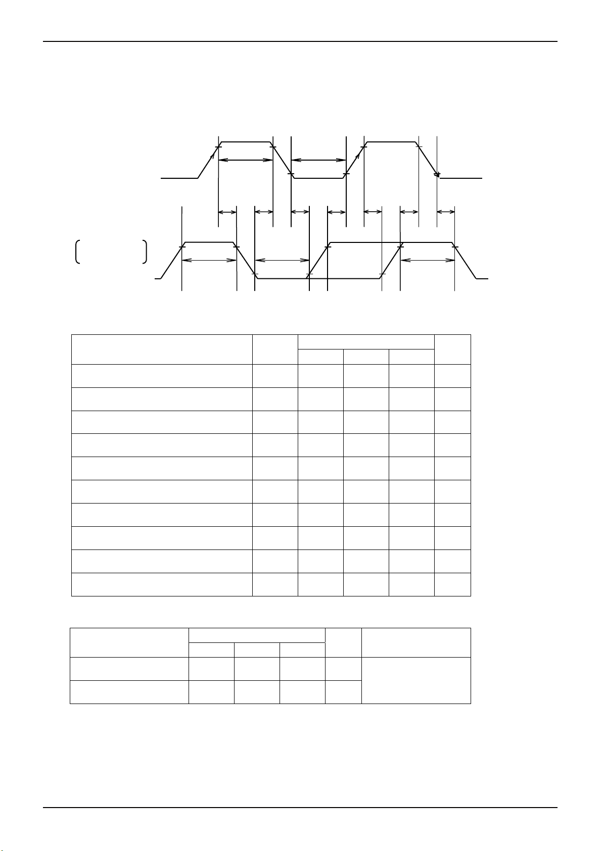
●Timing chart
1) Signal Timing Conditions
・Data is read on the rising edge of the clock.
・Latch is read on the falling edge of the clock.
・Latch signal must terminate with the LOW state.
*To avoid malfunctions, clock and data signals must terminate with the LOW state.
(CLOCK)
CL
90% 90% 90% 90%
twc
10% 10% 10%
twc
thd thdth ts tsl thl tsd
DA
DATA
LATCH
90% 90% 90%
twd
DATA DATA
twh
10%
Fig.1
Parameter Symbol
Min. Typ. Max.
Limits
90% 90%
twl
10% 10%
LATCH
Unit
Technical Note
Terminate with
LOW
Minimum Clock Width twc 1.0 - - µs
Minimum Data Width twd 1.0 - - µs
Minimum Latch Width twl 1.0 - - µs
LOW Hold Width twh 1.0 - - µs
Data Set-up Time (DATACLK) tsd 0.5 - - µs
Data Hold Time (CLKDATA) thd 0.5 - - µs
Latch Set-up Time (CLKLATCH) tsl 0.5 - - µs
Latch Hold Time (DATALATCH) thl 0.5 - - µs
Latch Low Set-up Time ts 0.5 - - µs
Latch Low Hold Time th 0.5 - - µs
2) Voltage Conditions for Control Signals
Parameter
Limits
Min. Typ. Max.
Unit Conditions
“H” Input Voltage 2.2 - 5.5 V
“L” Input Voltage 0 - 1.0 V
www.rohm.com
© 2010 ROHM Co., Ltd. All rights reserved.
3/9
Vcc = 6.5~7.3V
VEE=-6.5~-7.3V
2010.06 - Rev.A

BD3452KS
3) Basic Configuration of Control Data Formats
Input direction
MSB
D16 D15 D14 D13 D12 D11 D10 D9 D8 D7 D6 D5 D4 D3 D2 D1 D0
Data
・Control Data Formats
Input direction
D16 D15 D14 D13 D12 D11 D10 D9 D8 D7 D6 D5 D4 D3 D2 D1 D0
Data
(1)
Data
(2)
Data
(3)
Data
(4)
Input selector 1 Input selector 2 Input ATT Input gain * * 0 0 0
D16 D15 D14 D13 D12 D11 D10 D9 D8 D7 D6 D5 D4 D3 D2 D1 D0
FLR Input
Selector
D16 D15 D14 D13 D12 D11 D10 D9 D8 D7 D6 D5 D4 D3 D2 D1 D0
Output gain 7ch Output gain SWch * * * * * 1 0 0 1
D16 D15 D14 D13 D12 D11 D10 D9 D8 D7 D6 D5 D4 D3 D2 D1 D0
Master volume FLch Master volume FRch 0 1 0
SBLR Input
Selector
Technical Note
Data Select Address
Select Address
Multi Input
Selector
RECA RECB Port A Port
B
* 0 0 0 1
LSB
D16 D15 D14 D13 D12 D11 D10 D9 D8 D7 D6 D5 D4 D3 D2 D1 D0
Data
(5)
Data
(6)
Data
(7)
By changing the setting of Select Address, seven different control formats are selectable.
For Select Address, the values except those shown above must not be specified.
Each time of power-on, all of the address data must be initialized.
* indicates 0 or 1.
(Example)
MSB LSB MSB LSB MSB LSB MSB LSB MSB LSB MSB LSB MSB LSB
Data(1) L Data(2) L Data(3) L Data(4) L Data(5) L Data(6) L Data(7) L
“L” means latch.
After power-on, for the second and subsequent times, only the desired data can be selected for setting.
(Example) When changing Output Gain SWch,Input direction
Master volume Cch Master volume SWch 0 1 1
D16 D15 D14 D13 D12 D11 D10 D9 D8 D7 D6 D5 D4 D3 D2 D1 D0
Master volume SLch Master volume SRch 1 1 0
D16 D15 D14 D13 D12 D11 D10 D9 D8 D7 D6 D5 D4 D3 D2 D1 D0
Master volume SBLch Master volume SBRch 1 1 1
Input direction
MSB LSB
Data(3) L
“L” means latch.
www.rohm.com
© 2010 ROHM Co., Ltd. All rights reserved.
4/9
2010.06 - Rev.A
BD3452KS
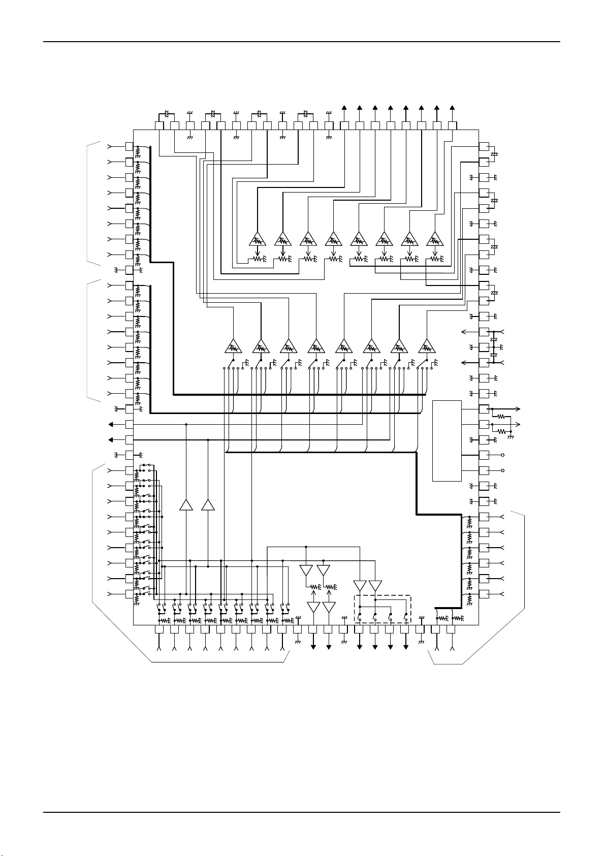
●Application circuit
FL
FR
C
SL
SR
SBL
SBR
SW
FL
FR
8ch Input 8ch Input
SL
SR
SBL
SBR
SW
BOUT1
BOUT2
10
11
C
12
13
15
16
17
18
19
20
21
L
22
R
23
L
24
25
R
L
26
R
27
L
28
29
R
L
30
Technical Note
OUTC
Volume
SBL
Gain
45 46
OUTSL
OUTSBL
OUTSR
84
OUTSBR
OUTSW
83
82
80
+
10µ
79
78
77
+
10µ
76
75
Gain
Gain
Output
Volume
Gain
Output
Output
Volume
74
+
10µ
73
72
71
+
10µ
70
69
R
SB
Gain
Input
VEE
S
W
Gain
Input
VCC
68
67
66
+
+
47µ
47µ
VEE
VCC
65
64
logic
63
62
61
60
59
58
10K
10K
DA
CL
DGN
D
PORTB
PORTA
57
SW
56
47K
SBR
55
47K
SBL
54
47K
SR
53
47K
SL
52
REC
47K 47K
49
4847
FL
ROUTA2
ROUTB2
ROUTB1
47K
C
51
47K
50
8ch Input (DSP)
FR
UNIT
RESISTOR : Ω
CAPACITOR : F
OUTFL
10µ
+
100
99 95
1
47K
2
47K
3
47K
4
47K
5
47K
6
47K
7
47K
8
47K
10µ
+
9698 97 81
10µ
+
10µ
+
94 93 899092 91 88
Gain
Gain
Gain
Output
Output
Volume
Volume
Volume
Gain
Output
Output
Volume
OUTFR
87 86 85
Gain
Output
Volume
9
47K
47K
47K
47K
1
4
47K
47K
47K
47K
47K
47K
47K
47K
47K
47K
47K
47K
47K
47K 47K 47K 47K 47K 47K 47K 47K 47K
31
32
33 34
R
L
R
9ch Input Selector
FL
Gain
Gain
Input
Input
36
35
L
37 38
R
R
L
C
FR
Gain
Input
39 40
L
SL
42
AOUT1
Gain
Input
43
AOUT2
SR
Input
44
ROUTA1
Gain
Input
ATT
Input
41
R
Fig.2
www.rohm.com
© 2010 ROHM Co., Ltd. All rights reserved.
5/9
2010.06 - Rev.A

BD3452KS
●Reference data
25
20
15
10
5
0
-5
-10
-15
CIRCUIT CURRENT (mA)
-20
0246810
POWER SUPPLY (V)
Fig.3 Circuit Current - Power Supply
VCC
VEE
10
8
6
4
2
0
-2
GAIN (dB)
-4
-6
-8
-10
10 100 1000 10000 100000
FREQUENCY (Hz)
Fig.4 Voltage Gain - Frequency
Technical Note
10
1
0.1
0.01
OUTPUT VOLTAGE (Vrms)
0.001
0.001 0.01 0.1 1 10
IN PUT VOLTAGE (Vrms)
Fig.5 Output Voltage - Input Voltage
10
1
0.1
0.01
THD+N (%)
0.001
0.0001
0.001 0.01 0.1 1 10
INPUT VOLTAGE (Vrms)
Fig.6 THD+N - Input Voltage
0
-10
-20
-30
-40
-50
-60
-70
-80
-90
OUTPUT ATTENUATION (dB)
-100
-100 -80 -60 -40 -20 0
VOLUME DATA (dB)
Fig.9 Volume Attenuation -
Volume Settin
2
0
-2
-4
-6
-8
GAIN (dB)
-10
-12
-14
10 100 1000 10000 100000
FREQUENCY (Hz)
Fig.7 Input Attenuation - Frequency
16
14
12
10
8
6
GAIN (dB)
4
2
0
-2
10 100 1000 10000 100000
15dB
10dB
5dB
0dB
FREQUENCY (Hz)
Fig.10 Output Gain - Frequency
14
12
10
8
6
4
GAIN (dB)
2
0
-2
10 100 1000 10000 100000
12dB
6dB
0dB
FREQUENCY (Hz)
Fig.8 Input Gain - Frequency
0
-20
-40
-60
-80
CROSSTALK (dB)
-100
-120
10 100 1000 10000 100000
FREQUENCY (Hz)
Fig.11 Cross-talk between Channels -
Frequency
0
-20
-40
-60
-80
CR OSSTALK (dB)
-100
-120
10 100 1000 10000 100000
FREQUENCY (Hz)
Fig.12 Cross-talk between Selectors -
Frequency
www.rohm.com
© 2010 ROHM Co., Ltd. All rights reserved.
5.0
4.5
4.0
3.5
3.0
2.5
2.0
1.5
NOISE (μVrm s)
1.0
0.5
0.0
246810
POWER SU PPLY (V)
Fig.13 Output Noise Voltage -
Power Supply Voltage
6/9
6
5
4
3
2
PORT VOLTAGE (V)
1
0
110100
IMPEDANCE (Ω)
Fig.14 Port H Voltage –
Load Resistance
2010.06 - Rev.A

BD3452KS
●Notes for use
(1) Numbers and data in entries are representative design values and are not guaranteed values of the items.
(2) Although we are confident in recommending the sample application circuits, carefully check their characteristics further
when using them. When modifying externally attached component constants before use, determine them so that they have
sufficient margins by taking into account variations in externally attached components and the Rohm LSI, not only for static
characteristics but also including transient characteristics.
(3) Absolute maximum ratings
If applied voltage, operating temperature range, or other absolute maximum ratings are exceeded, the LSI may be
damaged. Do not apply voltages or temperatures that exceed the absolute maximum ratings. If you think of a case in
which absolute maximum ratings are exceeded, enforce fuses or other physical safety measures and investigate how not
to apply the conditions under which absolute maximum ratings are exceeded to the LSI.
(4) VEE potential
Make the VEE pin voltage such that it is the lowest voltage even when operating below it. Actually confirm that the voltage
of each pin does not become a lower voltage than the VEE pin, including transient phenomena.
(5) Thermal design
Perform thermal design in which there are adequate margins by taking into account the allowable power dissipation in
actual states of use.
(6) Shorts between pins and misinstallation
When mounting the LSI on a board, pay adequate attention to orientation and placement discrepancies of the LSI. If it is
misinstalled and the power is turned on, the LSI may be damaged. It also may be damaged if it is shorted by a foreign
substance coming between pins of the LSI or between a pin and a power supply or a pin and a GND.
(7) Operation in strong magnetic fields
Adequately evaluate use in a strong magnetic field, since there is a possibility of malfunction.
(8) About Operating Voltage Range and Operating Temperature Range
The circuit functional operations are guaranteed within the Operating Voltage Range and Operating Temperature Range.
The standard values of electrical characteristics, however, are guaranteed under the specific conditions. Accordingly,
careful consideration of the IC characteristic variations is required to design a set of circuit.
(9) About power ON/OFF
(a) At power ON/OFF, a shock sound will be generated and, therefore, use MUTE on the set.
(b) When turning on power supplies, VEE and VCC should be powered on simultaneously or VEE first;
then followed by VCC. If the VCC side is started up first, an excessive current may pass VCC through VEE.
(10) About serial control
For the CL and DA terminals, the patterned and other wirings should be routed not to cause interference with the
analog-signal-related lines.
(11) About function switching
When switching Input Selector or Input Gain, use MUTE on Master Volume.
Technical Note
www.rohm.com
© 2010 ROHM Co., Ltd. All rights reserved.
7/9
2010.06 - Rev.A
BD3452KS
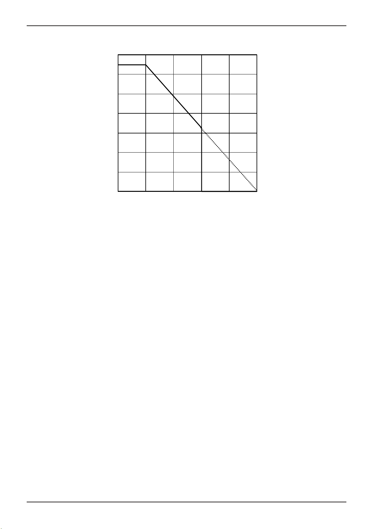
●Thermal derating characteristic
1400
1200
1000
800
600
400
Power Dissipation Pd (mW)
200
0
BD3452KS
ROHM standard board packaging time value
Board size: 70 x 70 x 1.6mm Raw material : FR4 glass epoxy board (copper area 3% or below)
Technical Note
1300mW
0 25 50 75 100 125
Ta(℃)
Fig.15
www.rohm.com
© 2010 ROHM Co., Ltd. All rights reserved.
8/9
2010.06 - Rev.A
BD3452KS
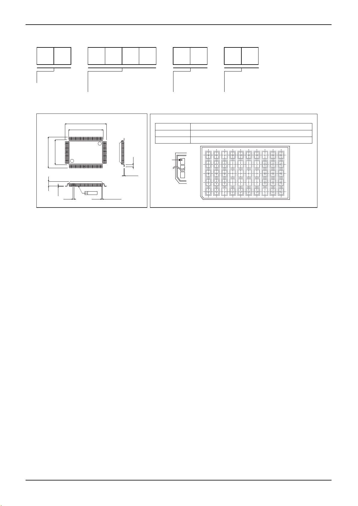
●Ordering part number
Technical Note
B D
3 4 5 2 K S -
Part No. Part No. Package
SQFP100
81
14.0±0.2
18.0±0.3
100
2.7±0.1
0.05
0.65
24.0±0.3
20.0±0.2
0.15
51
30
0.3±0.1
50
31
1.2
0.15±0.1
(Unit : mm)
80
1
<Tape and Reel information>
Quantity
Direction of feed
1pin
KS: SQFP100
Tray (with dry pack)Container
500pcs
Direction of product is fixed in a tray
Order quantity needs to be multiple of the minimum quantity.
∗
Packaging and forming specification
None :Tray
www.rohm.com
© 2010 ROHM Co., Ltd. All rights reserved.
9/9
2010.06 - Rev.A

Notes
No copying or reproduction of this document, in part or in whole, is permitted without the
consent of ROHM Co.,Ltd.
The content specied herein is subject to change for improvement without notice.
The content specied herein is for the purpose of introducing ROHM's products (hereinaf ter
"Products"). If you wish to use any such Product, please be sure to refer to the specications,
which can be obtained from ROHM upon request.
Examples of application circuits, circuit constants and any other information contained herein
illustrate the standard usage and operations of the Products. The peripheral conditions must
be taken into account when designing circuits for mass production.
Great care was taken in ensuring the accuracy of the information specied in this document.
However, should you incur any damage arising from any inaccuracy or misprint of such
information, ROHM shall bear no responsibility for such damage.
The technical information specied herein is intended only to show the typical functions of and
examples of application circuits for the Products. ROHM does not grant you, explicitly or
implicitly, any license to use or exercise intellectual property or other rights held by ROHM and
other parties. ROHM shall bear no responsibility whatsoever for any dispute arising from the
use of such technical information.
Notice
The Products specied in this document are intended to be used with general-use electronic
equipment or devices (such as audio visual equipment, ofce-automation equipment, communication devices, electronic appliances and amusement devices).
The Products specied in this document are not designed to be radiation tolerant.
While ROHM always makes efforts to enhance the quality and reliability of its Products, a
Product may fail or malfunction for a variety of reasons.
Please be sure to implement in your equipment using the Products safety measures to guard
against the possibility of physical injury, re or any other damage caused in the event of the
failure of any Product, such as derating, redundancy, re control and fail-safe designs. ROHM
shall bear no responsibility whatsoever for your use of any Product outside of the prescribed
scope or not in accordance with the instruction manual.
The Products are not designed or manufactured to be used with any equipment, device or
system which requires an extremely high level of reliability the failure or malfunction of which
may result in a direct threat to human life or create a risk of human injury (such as a medical
instrument, transportation equipment, aerospace machinery, nuclear-reactor controller, fuelcontroller or other safety device). ROHM shall bear no responsibility in any way for use of any
of the Products for the above special purposes. If a Product is intended to be used for any
such special purpose, please contact a ROHM sales representative before purchasing.
If you intend to export or ship overseas any Product or technology specied herein that may
be controlled under the Foreign Exchange and the Foreign Trade Law, you will be required to
obtain a license or permit under the Law.
Thank you for your accessing to ROHM product informations.
More detail product informations and catalogs are available, please contact us.
ROHM Customer Support System
www.rohm.com
© 2010 ROHM Co., Ltd. All rights reserved.
http://www.rohm.com/contact/
R1010
A
 Loading...