TECHNICAL NOTE
Power Management LSI Series for Automotive Body Control
Regulators with
Voltage Detector and
W atchdog Timer
BD3004HFP,BD3005HFP
zDescription
The BD3004HFP,BD3005HFP low bias current regulator and watchdog timer features a high 50 V breakdown voltage and is compatible
with on-board vehicle microcontrollers. It offers an output current of 500 mA while limiting bias current to 80 µA (Typ.). The series supports
the use of ceramic capacitors as output phase compensation capacitors.The reset detection voltage can be changed by connecting a
resistor to the Vs pin.(BD3004HFP)The watchdog timer can be switched on and off using the INH pin input logic.(BD3005HFP)
zFeatures
1) 5 V/500 mA regulators for microcontrollers
BD3004HFP: Adjustable detection voltage (Vs pin)
BD3005HFP:Built-in watchdog timer reset circuit (INH pin: watchdog timer on/off)
2) Super-low bias current: 80 µA (Typ.)
3) Low-saturation voltage type P-channel DMOS output transistors
4) High precision output voltage: 5 V ±2%
5) Low-ESR ceramic capacitors can be used as output capacitors
6) Vcc Maximum applied voltage: 50 V
7) Built-in overcurrent protection circuit and thermal shutdown circuit
8) Built-in reverse connection breakdown prevention circuit
9) Back current flow protection during sudden battery failures, making it a highly reliable 5 V regulator.
10) HRP7 package
zApplications
Onboard devices (Vehicle equipment, Car stereos, Satellite navigation systems, etc.)
zAbsolute maximum ratings (Ta = 25°C)
Parameter Symbol Limit Unit
Vcc applied voltage Vcc 15 to +50*1 V
Vs pin voltage(BD3004HFP) Vs 0.3 to +15 V
INH pin voltage(BD3005HFP) VINH 0.3 to +15 V
Regulator output pin voltage VOUT 0.3 to +15 V
Reset output pin voltage VRO 0.3 to +15 V
Watchdog input pin voltage VCLK 0.3 to +15 V
Reset delay setting pin voltage VCT 0.3 to +15 V
Output current IOUT 500 mA
Power dissipation Pd 1.6*2 W
Operating temperature range Topr 40 to +125 °C
Storage temperature range Tstg 55 to +150 °C
Maximum junction temperature Tjmax 150 °C
*1 Must not exceed Pd.
*2 Reduced by 12.8 mW/°C over 25°C, when mounted on a glass epoxy board (70 mm × 70 mm × 1.6 mm).
Ver.B July 2006

zOperating power supply voltage range (Ta = 25°C)
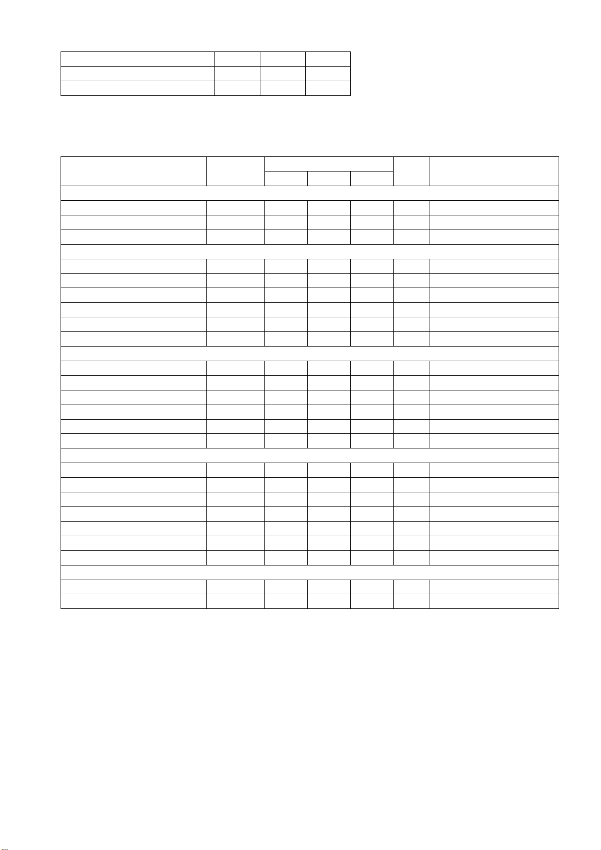
Parameter Min. Max. Unit
Operating power supply voltage range 5.5* 36** V
Output current - 500 mA
* For the output voltage, consider the voltage drop (min. I/O voltage differential) due to the output current.
** Must not exceed Pd.
zElectrical Characteristics (Unless otherwise specified, Ta = 40°C to 125°C, Vcc = 13.5 V)
Parameter Symbol
[Overall]
Total supply current 1 Icc1 — 80 130 µA Io=0mA
Total supply current 2 Icc2 — 80 130 µA Io=200mA
Total supply current 3(BD3005HFP) Icc3 — 80 130 µA VINH=0V
[Regulator]
Output voltage VOUT 4.90 5.00 5.10 V
Input stability Line.Reg — 10 20 mV Vcc=6.2~25 V
Load stability
Min. I/O voltage differential
Output current
Ripple rejection
[Reset]
Detection voltage(BD3004HFP)
Detection voltage(BD3005HFP) Vdet 4.40 4.50 4.60 V
Hysteresis width VHS 50 100 150 mV
Output delay time Low → High TdLH 12 21 40 mS CT=0.1µF*1
Low output voltage VRST — 0.2 0.5 V IRST=2mA
Min. operating voltage VOPL 1.0 — — V
[Watchdog timer]
High-side switching threshold voltage VthH 1.16 1.26 1.36 V
Low-side switching threshold voltage VthL 0.20 0.24 0.28 V
Discharge current Ictc 1 2 3 µA
Charge current Icto 3 6 10 µA
Watchdog monitor time TWH 32 51 90 mS CT=0.1µF*2
Watchdog reset time TWL 10 17 30 mS CT=0.1µF*3
Clock input pulse width TWCLK 500 — — nS
[INH]
WDT off voltage(BD3005HFP) VUINH 3.2 — 8.0 V
WDT on voltage(BD3005HFP) VLINH 0 — 1.8 V
*1 TdLH can be varied by changing the CT capacitance value.
TdLH (s) ≈ (1.26 × CT (µF)) / Icto (µA) (Calculation uses Typ. values)
*2 TWH can be varied by changing the CT capacitance value.
TWH (s) ≈ (1.02 × CT (µF)) / Ictc (µA) (Calculation uses Typ. values)
*3 TWL can be varied by changing the CT capacitance value.
TWL (s) ≈ (1.02 × CT (µF)) / Icto (µA) (Calculation uses Typ. values)
Note: This IC is not designed to be radiation-resistant.
Load.Reg — 15 30 mV Io=5~200mA
Vd — 0.78 1.1 V Vcc=4.75 V, Io=200mA
IOUT 500 — — mA VOUT=4.9V
R.R. 45 55 — dB f=120Hz, ein=1Vrms, Io=200mA
Vdet 4.02 4.10 4.18 V
Min. Typ. Max.
Limit
Unit Conditions
2/8

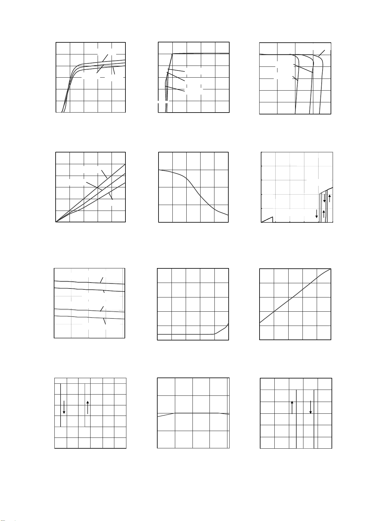
zReference data (Unless otherwise specified, Ta = 25°C)
120
100
Ta=125℃
80
60
40
Ta=25℃
Ta=-40℃
20
CIRCUIT CURRENT: Icc [µA]
0
0 5 10 15 20 25
SUPPLY VOLTAGE: Vcc [V]
Fig. 1 Circuit Current
3
2.5
2
1.5
1
0.5
Ta=125℃
Ta=25℃
DROPOUT VOLTAGE: Vd [V]
0
0 100 200 300 400 500
OUTPUT CURRENT: IOUT [mA]
Fig. 4 I/O Voltage Difference
Ta=-40℃
RIPPLE REJECTON: R.R. [dB]
4.8
4.6
4.4
4.2
4.0
DETECTION VOLTAGE: [V]
3.8
BD3005HFP
BD3004HFP
-40 0
Rising Edge Detection Voltage
Falling Edge Detection Voltage
Rising Edge Detection Voltage
Falling Edge Detection Voltage
40 80 120
AMBIENT TEMPERA TURE:Ta[℃]
Fig. 7 Reset Detection Voltage
Temperature
0.5
0.4
0.3
0.2
0.1
CIRCUIT CURRENT: Icc [mA]
2
0
-2
-4
5.25
-6
-8
CT PIN CURRENT: ICT [µA]
-10
0 0.5 1 1.5 2 2.5 3
CT PIN VOLTAGE: VC T [V]
Fig. 10 CT Pin Charge vs
Discharge Current
4.75
OUTPUT VOLTAGE: VOUT [V]
6
5
4
3
2
1
Ta=-40℃
Ta=25℃
Ta=125℃
OUTPUT VOLTAGE: VOUT [V]
0
0 5 10 15 20 25
SUPPLY VOLTAGE: Vcc [V]
Fig. 2 Output Voltage vs
Supply Voltage
80
60
40
20
0
10 100 1000 10000 100000 1E+06
FREQUENCY: f [Hz]
Fig. 5 Ripple Rejection
0
0 100 200 300 400 500
OUTPUT CURRENT: IOUT [mA]
Fig. 8 Total Supply Current
Classified by Load
5.5
5
4.5
-40 0 40 80 120
AMBIENT TEMPER ATUR E: Ta [℃]
Fig. 11 Output Voltage vs
Temperature
3/8
6
5
4
3
2
1
Ta=25℃
Ta=125℃
Ta=-40℃
OUTPUT VOLTAGE: VOUT [V]
0
0 500 1000 1500 2000
OUTPUT CURRENT: IOUT [mA]
Fig. 3 Output Voltage vs Load
10
8
6
4
2
RESET VOLTAGE: VRESET[V]
0
0
1 2 3 4 5
OUTPUT VOLTAGE: VOUT [V]
Fig. 6 Reset Detection Voltage
0
-10
-20
-30
-40
CIRCIT CURRENT: Icc [µA]
-50
-15 -12 -9 -6 -3 0
BD3005HFP
BD3004HFP
SUPPLY VOLTAGE: Vcc [V]
Fig. 9 Back Current
6
5
4
3
2
1
OUTPUT VOLTAGE: VOUT [V]
0
100 120 140 160 180 200
AMBIENT TEMPERATUR E: Ta [℃]
Fig. 12 Thermal Shutdown
Circuit
 Loading...