

TECHNICAL NOTE
Power Management LSI Series for Automotive Body Control
Regulators with
Voltage Detector and
W atchdog Timer
BD3004HFP,BD3005HFP
zDescription
The BD3004HFP,BD3005HFP low bias current regulator and watchdog timer features a high 50 V breakdown voltage and is compatible
with on-board vehicle microcontrollers. It offers an output current of 500 mA while limiting bias current to 80 µA (Typ.). The series supports
the use of ceramic capacitors as output phase compensation capacitors.The reset detection voltage can be changed by connecting a
resistor to the Vs pin.(BD3004HFP)The watchdog timer can be switched on and off using the INH pin input logic.(BD3005HFP)
zFeatures
1) 5 V/500 mA regulators for microcontrollers
BD3004HFP: Adjustable detection voltage (Vs pin)
BD3005HFP:Built-in watchdog timer reset circuit (INH pin: watchdog timer on/off)
2) Super-low bias current: 80 µA (Typ.)
3) Low-saturation voltage type P-channel DMOS output transistors
4) High precision output voltage: 5 V ±2%
5) Low-ESR ceramic capacitors can be used as output capacitors
6) Vcc Maximum applied voltage: 50 V
7) Built-in overcurrent protection circuit and thermal shutdown circuit
8) Built-in reverse connection breakdown prevention circuit
9) Back current flow protection during sudden battery failures, making it a highly reliable 5 V regulator.
10) HRP7 package
zApplications
Onboard devices (Vehicle equipment, Car stereos, Satellite navigation systems, etc.)
zAbsolute maximum ratings (Ta = 25°C)
Parameter Symbol Limit Unit
Vcc applied voltage Vcc 15 to +50*1 V
Vs pin voltage(BD3004HFP) Vs 0.3 to +15 V
INH pin voltage(BD3005HFP) VINH 0.3 to +15 V
Regulator output pin voltage VOUT 0.3 to +15 V
Reset output pin voltage VRO 0.3 to +15 V
Watchdog input pin voltage VCLK 0.3 to +15 V
Reset delay setting pin voltage VCT 0.3 to +15 V
Output current IOUT 500 mA
Power dissipation Pd 1.6*2 W
Operating temperature range Topr 40 to +125 °C
Storage temperature range Tstg 55 to +150 °C
Maximum junction temperature Tjmax 150 °C
*1 Must not exceed Pd.
*2 Reduced by 12.8 mW/°C over 25°C, when mounted on a glass epoxy board (70 mm × 70 mm × 1.6 mm).
Ver.B July 2006

zOperating power supply voltage range (Ta = 25°C)
Parameter Min. Max. Unit
Operating power supply voltage range 5.5* 36** V
Output current - 500 mA
* For the output voltage, consider the voltage drop (min. I/O voltage differential) due to the output current.
** Must not exceed Pd.
zElectrical Characteristics (Unless otherwise specified, Ta = 40°C to 125°C, Vcc = 13.5 V)
Parameter Symbol
[Overall]
Total supply current 1 Icc1 — 80 130 µA Io=0mA
Total supply current 2 Icc2 — 80 130 µA Io=200mA
Total supply current 3(BD3005HFP) Icc3 — 80 130 µA VINH=0V
[Regulator]
Output voltage VOUT 4.90 5.00 5.10 V
Input stability Line.Reg — 10 20 mV Vcc=6.2~25 V
Load stability
Min. I/O voltage differential
Output current
Ripple rejection
[Reset]
Detection voltage(BD3004HFP)
Detection voltage(BD3005HFP) Vdet 4.40 4.50 4.60 V
Hysteresis width VHS 50 100 150 mV
Output delay time Low → High TdLH 12 21 40 mS CT=0.1µF*1
Low output voltage VRST — 0.2 0.5 V IRST=2mA
Min. operating voltage VOPL 1.0 — — V
[Watchdog timer]
High-side switching threshold voltage VthH 1.16 1.26 1.36 V
Low-side switching threshold voltage VthL 0.20 0.24 0.28 V
Discharge current Ictc 1 2 3 µA
Charge current Icto 3 6 10 µA
Watchdog monitor time TWH 32 51 90 mS CT=0.1µF*2
Watchdog reset time TWL 10 17 30 mS CT=0.1µF*3
Clock input pulse width TWCLK 500 — — nS
[INH]
WDT off voltage(BD3005HFP) VUINH 3.2 — 8.0 V
WDT on voltage(BD3005HFP) VLINH 0 — 1.8 V
*1 TdLH can be varied by changing the CT capacitance value.
TdLH (s) ≈ (1.26 × CT (µF)) / Icto (µA) (Calculation uses Typ. values)
*2 TWH can be varied by changing the CT capacitance value.
TWH (s) ≈ (1.02 × CT (µF)) / Ictc (µA) (Calculation uses Typ. values)
*3 TWL can be varied by changing the CT capacitance value.
TWL (s) ≈ (1.02 × CT (µF)) / Icto (µA) (Calculation uses Typ. values)
Note: This IC is not designed to be radiation-resistant.
Load.Reg — 15 30 mV Io=5~200mA
Vd — 0.78 1.1 V Vcc=4.75 V, Io=200mA
IOUT 500 — — mA VOUT=4.9V
R.R. 45 55 — dB f=120Hz, ein=1Vrms, Io=200mA
Vdet 4.02 4.10 4.18 V
Min. Typ. Max.
Limit
Unit Conditions
2/8
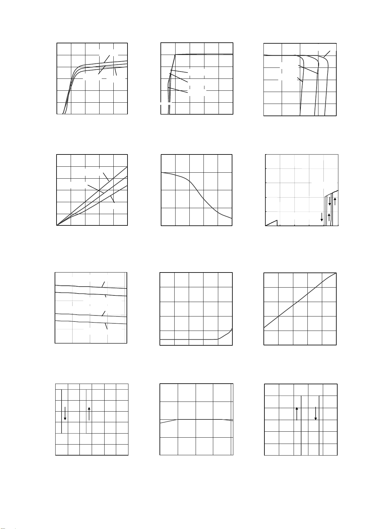
zReference data (Unless otherwise specified, Ta = 25°C)
120
100
Ta=125℃
80
60
40
Ta=25℃
Ta=-40℃
20
CIRCUIT CURRENT: Icc [µA]
0
0 5 10 15 20 25
SUPPLY VOLTAGE: Vcc [V]
Fig. 1 Circuit Current
3
2.5
2
1.5
1
0.5
Ta=125℃
Ta=25℃
DROPOUT VOLTAGE: Vd [V]
0
0 100 200 300 400 500
OUTPUT CURRENT: IOUT [mA]
Fig. 4 I/O Voltage Difference
Ta=-40℃
RIPPLE REJECTON: R.R. [dB]
4.8
4.6
4.4
4.2
4.0
DETECTION VOLTAGE: [V]
3.8
BD3005HFP
BD3004HFP
-40 0
Rising Edge Detection Voltage
Falling Edge Detection Voltage
Rising Edge Detection Voltage
Falling Edge Detection Voltage
40 80 120
AMBIENT TEMPERA TURE:Ta[℃]
Fig. 7 Reset Detection Voltage
Temperature
0.5
0.4
0.3
0.2
0.1
CIRCUIT CURRENT: Icc [mA]
2
0
-2
-4
5.25
-6
-8
CT PIN CURRENT: ICT [µA]
-10
0 0.5 1 1.5 2 2.5 3
CT PIN VOLTAGE: VC T [V]
Fig. 10 CT Pin Charge vs
Discharge Current
4.75
OUTPUT VOLTAGE: VOUT [V]
6
5
4
3
2
1
Ta=-40℃
Ta=25℃
Ta=125℃
OUTPUT VOLTAGE: VOUT [V]
0
0 5 10 15 20 25
SUPPLY VOLTAGE: Vcc [V]
Fig. 2 Output Voltage vs
Supply Voltage
80
60
40
20
0
10 100 1000 10000 100000 1E+06
FREQUENCY: f [Hz]
Fig. 5 Ripple Rejection
0
0 100 200 300 400 500
OUTPUT CURRENT: IOUT [mA]
Fig. 8 Total Supply Current
Classified by Load
5.5
5
4.5
-40 0 40 80 120
AMBIENT TEMPER ATUR E: Ta [℃]
Fig. 11 Output Voltage vs
Temperature
3/8
6
5
4
3
2
1
Ta=25℃
Ta=125℃
Ta=-40℃
OUTPUT VOLTAGE: VOUT [V]
0
0 500 1000 1500 2000
OUTPUT CURRENT: IOUT [mA]
Fig. 3 Output Voltage vs Load
10
8
6
4
2
RESET VOLTAGE: VRESET[V]
0
0
1 2 3 4 5
OUTPUT VOLTAGE: VOUT [V]
Fig. 6 Reset Detection Voltage
0
-10
-20
-30
-40
CIRCIT CURRENT: Icc [µA]
-50
-15 -12 -9 -6 -3 0
BD3005HFP
BD3004HFP
SUPPLY VOLTAGE: Vcc [V]
Fig. 9 Back Current
6
5
4
3
2
1
OUTPUT VOLTAGE: VOUT [V]
0
100 120 140 160 180 200
AMBIENT TEMPERATUR E: Ta [℃]
Fig. 12 Thermal Shutdown
Circuit
zBlock diagram
K
OUT
Vcc
Cin
Vs
(BD3004HFP)
INH
(BD3005HFP)
3
2
2
Pre Reg
Reverse Polarity Protection
Vref
TSD
OCP
OUT
OUT
OUT
5
Co
HRP7
FIN
RESET
Cin: 0.33 µF to 1000 µF
Signal from
microcontroller
Co: 0.1 µF to 1000 µF
CT: 0.001 µF to 22 µF
CL
GND
1
4
FIN
WDT
6
CT
7
CT
1 2 3 4 5 6 7
Fig.13
zPin descriptions
Pin. No
1
2
3
4
5
6
Pin name
CLK
Vs(BD3004HFP)
INH(BD3005HFP)
Vcc
GND
OUT
RESET
Function
Clock input from microcontroller
Reset
detection voltage adjustment function pin
WDT on/off function pin (WDT off when INH = high; WDT on when INH = low)
Power supply pin
GND pin
Voltage output pin
Reset output pin
7 CT Reset output delay time, WDT monitor time setting external capacitance connection pin
FIN
GND
GND pin
zI/O Circuit diagram
CLK (1 pin) Vs(2 pin) INH (2 pin)
Vcc
PREREG
Vcc
PREREG
Vcc
PREREG
Ω
CLK
100KΩ
Vs
OUT (5 pin) RESET (6 pin)
OUT
Vcc
RESET
Rb
Ra
100KΩ
OUT
Fig.14
3.56M
1.56MΩ
470KΩ
OUT
INH
100KΩ
CT (7 pin)
OUT
CT
OUT
* All resistance values are typical ones.
4/8
● Detection voltage adjustment
R4
Vs Detection voltage
1,25V(Typ.)
R3
OUT
For a basic detection voltage of 4.1 V,
R2=3.56MΩ
To change the detection voltage,
insert pull-down resistor R3 (with a resistance value lower than R1)
R1=1.56MΩ
between the Vs and GND pins, and pull-up resistor R4 (with a
resistance value lower than R2) between the Vs and Vo pins.
(All resistance values are typical ones.)
Vdet = Vs × (R1 + R2 / R1)
Vdet = Vs × (R3 + R4 / R3) [R3<<R1, R4<<R2]
Fig.15
zTiming chart
Vcc
VOUT
VINH
0
VdetH
Vdet
0
0
When VINH = high
WDT current off
VHS
VdetH = Vdet + VHS
CLK
VCT
0
VthH
VthL
0
TdLH
TWL
TWH
TWCLK
TWCLK
RESET
0
(1)
(2)
(3)
(4) (7) (5)
(6)
(4)
(8) (9) (10)
(5)
(4)
(5)
(2)
(3)
(10)(2) (4)
(3)
(5)
(10)
(11)
Fig.16
zExplanation
(1) When the output voltage (VOUT) reaches 1.0 V, the reset pin voltage (RESET) will switch to low level.
(2) When VOUT reaches or exceeds the reset clear voltage (VdetH), the external capacitor connected to the CT pin will begin to charge.
When the CT pin voltage (VCT) reaches the upper switching threshold voltage (VthH), RESET will maintain a low-level signal. When
VCT reaches the VthH voltage, RESET will switch from low to high level. The time from VCT reaching or exceeding the VdetH voltage
until RESET reverses (the RESET transmission delay time: TdLH) is given by the following equation:
TdLH (s) ≈ (1.26 × CT (µF)) / Icto (µA)
[1]
(3) The watchdog timer operates when RESET rises.
(4) When VCT reaches the lower s witching threshold voltage (VthL), the CT pin switches from discharging to charging, and RESET
switches from high level to low level. The watchdog timer reset time TWL is given by the following equation:
TWL(s) ≈ (1.02 × CT (µF)) / Icto (µA)
[2]
(5) The CT pin state switches from charge to discharge when VCT reaches VthH, and RESET switches from low to high.
The watchdog timer monitor time TWH is given by the following equation:
TWH(s) ≈ (1.02 × CT (µF)) / Ictc (µA)
[3]
(6) The CT pin state may not switche from charge to discharge when the CLK input pulse width (TWCLK) is short.
Use a TWCLK input pulse width of at least 500 ns.
(7) When a pulse (positive edge trigger) of at least 500 ns is input to the CLK pin while the CT pin is discharging, VCT switches from
discharging to charging and then switches back to discharging once it charges to VthH.
(8) Watchdog timer operation is forced off when the INH pin switches to high. At that time, only the watchdog timer will be turned off, and
reset detection will operate normally.
(9) The watchdog timer function turns on when the INH pin switches to low. At that time, the external capacitor on the CT pin will be
discharged.
(10) RESET switches from high to low when OUT falls to the RESET detection voltage (VDET) or lower.
(11) When VOUT falls to 0 V, the RESET signal stays low until VOUT reaches 1.0 V
5/8

zSetting of heat
2.0
1.6
1.2
0.8
ROHM standard board
Board size: 70 mm
θja = 78.1 (°C /W)
× 70 mm × 1.6 mm
0.4
POWER DISSIPATON: Pd [W]
0
0 25 50 75
AMBIENT TEMPERA TURE: Ta [℃]
125
150100
Fig.17
Refer to the dissipation reduction illustrated in Fig.17 when using the IC in an environment where Ta 25°C. T he characteristics of the IC are
greatly influenced by the operating temperature. If the temperature exceeds the maximum junction temperature Tjmax, the elements of the IC
may be damaged. It is necessary to give sufficient consideration to the heat of the IC in view of two points, i.e., the protection of the IC from
instantaneous damage and the maintenance of the reliability of the IC in long-time operation.
In order to protect the IC from thermal destruction, the operating temperature of the IC must not exceed the maximum junction temperature
Tjmax. Fig.17 illustrates the power dissipation/heat mitigation characteristics for the HRP-7 package. Always operate the IC within the power
dissipation (Pd). The following method is used to calculate the power consumption Pc (W).
Pc = (Vcc VOUT) × IOUT + Vcc × Icc Vcc : Input voltage
Power dissipation Pd Pc VOUT : Output voltage
IOUT : Load current
The load current Io is obtained to operate the IC within the power dissipation. Icc : Total supply current
Pd – Vcc × Icc
IOUT
Vcc VOUT
For Icc, see Fig. 1.
From the above, the maximum load current IOUTmax for the applied voltage Vcc can be calculated during the thermal design process.
Calculation example
Example: at Ta = 85°C, Vcc = 12 V, VOUT = 5 V
0.832 12 × Icc
IOUT
12 5
IOUT 118 mA (Icc = 80 µA)
θja = 78.1°C/W → 12.8 mW/°C
25°C = 1.6 W → 85°C = 0.832 mW
Make a thermal calculation in consideration of the above equations so that the whole operating temperature range will be within the po wer
dissipation. The power consumption Pc of the IC, in the event of shorting (i.e., if the Vo and GND pins are shorted), will be obtained from the
following equation:
Pc = Vcc × (Icc + Ishort) Ishort = Short current
zExternal settings for pins and precautions
1) Vcc pin
Insert capacitors with a capacitance of 0.33 µF to 1,000 µF between the Vcc and GND pins.
The capacitance varies with the application. Be sure to design the capacitance with a sufficient margin.
2) Output pin
Capacitors for stopping oscillation must be placed between each output pin and the GND pin. Capacitor capacitance values can be
used in a range between 0.1 µF and 1,000 µF. Since oscillation does not occur even for ESR values from 0.001 Ω to 100 Ω, a ceramic
capacitor can be used. Abrupt input voltage and load fluctuations can affect output voltages. Output capacitor capacitance values
should be determined after sufficient testing of the actual application
3) CT pin
Be sure to connect a capacitor to the CT pin. The reset output delay time is given by equation (1) on P. 5. The WDT time is given by
equations (2) and (3) on P.5. The setting times are proportional to the capacitance value of CT pin from the equations, so the maximum
and minimum setting times can be calculated from the electrical characteristics according to the capacitance. Note however that the
electrical characteristics do not include the external capacitor's temperature characteristics. The recommended connection capacity for
the CT pin is 0.001 µF to 22 µF.
6/8

zOperation Notes
1. Absolute maximum ratings
An excess in the absolute maximum ratings, such as supply voltage, temperature range of operating conditions, etc., can
break down the devices, thus making impossible to identify breaking mode, such as a short circuit or an open circuit. If
any over rated values will expect to exceed the absolute ma ximum ratings, consider adding circuit protection devices,
such as fuses.
2. GND voltage
The potential of GND pin must be minimum potential in all operating conditions.
3. Thermal design
Use a thermal design that allows for a sufficient margin in light of the power dissipation (Pd) in actual operating conditions.
4. Inter-pin shorts and mounting errors
Use caution when positioning the IC for mounting on printed circuit boards. The IC may be damaged if there is any connection error or if
pins are shorted together.
5. Actions in strong electromagnetic field
Use caution when using the IC in the presence of a strong electromagnetic field as doing so may cause the IC to malfunction.
6. Testing on application boards
When testing the IC on an application board, connecting a capacitor to a pin with low impedance subjects the IC to stress. Always
discharge capacitors after each process or step. Always turn the IC's power supply off before connecting it to or removing it from a jig or
fixture during the inspection process. Ground the IC during assembly steps as an antistatic measure. Use similar precaution when
transporting or storing the IC.
7. Regarding input pin of the IC
This monolithic IC contains P+ isolation and P substrate layers between adjacent elements in order to keep them isolated.
P-N junctions are formed at the intersection of these P layers with the N layers of other elements, creating a parasitic diode or transistor.
For example, the relation between each potential is as follows:
When GND > Pin A and GND > Pin B, the P-N junction operates as a parasitic diode.
When GND > Pin B, the P-N junction operates as a parasitic transistor.
Parasitic diodes can occur inevitable in the structure of the IC. The operation of parasitic diodes can result in mutual interference among
circuits, operational faults, or physical damage. Accordingly, methods by which parasitic diodes operate, such as applying a voltage that
is lower than the GND (P substrate) voltage to an input pin, should not be used.
(Pin A)
Resistor
(Pin B)
N N
P
P
N
P+ P+
N N
Parasitic element
GND
Parasitic element
or transistor
Fig. 18 Example of IC structure
8. Ground Wiring Pattern
When using both small signal and large current GND patterns, it is recommended to isolate the two ground patterns, placing a single
ground point at the ground potential of application so that the pattern wiring resistance and voltage variations caused by large currents do
not cause variations in the small signal ground voltage. Be careful not to change the GND wiring pattern of any external components,
either.
9. Thermal shutdown circuit (TSD)
The IC incorporates a built-in thermal shutdown circuit (TSD circuit). The thermal shutdown circuit (TSD circuit) is designed only to shut
the IC off to prevent runaway thermal operation. It is not designed to protect the IC or guarantee its operation. Do not continue to use the
IC after operating this circuit or use the IC in an environment where the operation of this circuit is assumed.. (See Fig. 12)
10. Overcurrent protection circuit (OCP)
The IC incorporates a built-in overcurrent protection circuit that operates according to the output current capacity. This circ uit serves to
protect the IC from damage when the load is shorted. The protection circuit is designed to limit current flow by not latching i
and instantaneous current flow originating from a large capacitor or other component. These protection circuits are effective in
a large
preventing damage due to sudden and unexpected accidents. However, the IC should not be used in applications characterized by the
continuous operation or transitioning of the protection circuits. At the time of thermal designing, keep in mind that the current capability
has negative characteristics to temperatures. (See Fig. 3)
11. Negative surge application to Vcc pin
The IC incorporates a built-in reverse connection breakdown prevention circuit that prevents IC damage even if Vcc carries a lower
voltage than the GND pin. However, note that the absolute maximum rating for the negative power supply voltage is -15 V.
12. Back current flow when the Vcc power supply is suddenly interrupted
These ICs limit generation of back current flow when the Vcc power supply is suddenly interrupted to protect the IC from damage. Sinking
current is also limited, making the series compatible with designs where high-capacitance capacitors are used to lengthen the amount of
time over which the output voltage can be maintained.
Transistor (NPN)
C
P+
B
E
P
N
P substrate
GND
P+
(Pin B)
(Pin A)
C B
E
GND
Parasitic element or
transistor
Parasitic element
n the event of
7/8

zSelecting a model name when ordering
p
B
D 03
ROHM model
name
Part number
3004:Adjustable
detection voltage
3005:Stable
detection voltage
HRP7
<Dimension>
9.395 ± 0.125
(MAX 9.745 include BURR)
0.28.0
±
1.017
0.13
±
0.8875
0.05
±
0.08
8.82 – 0.1
(5.59)
765432S1
0.08
1.905 ± 0.1
(7.49)
4.5
0.27
S
0.73 ± 0.11.27
4 P
Package type
HFP: HRP7
<Tape and Reel informati on>
Tape
Quantity
Direction
of feed
Embossed carrier tape
cs
2000
TR
(The direction is the 1pin of product is at the upper light when you hold
reel on the left hand and you pull out the tape on the right hand)
x x x x x x x x x x x x x x x x x x x x x x x x
Reel
※When you order , please order in times the amount of package quantity.
0.13
±
0.15
0.2
±
±
10.54
1.523
0.835
+
5.5
-
4.5
+
0.1
-
0.05
(Unit:mm)
T R 0 F H
Taping
TR: Reel-wound embossed taping
1pin
Direction of feed
8/8
Catalog No.06T148A '06.7 ROHM C 1000 TSU

Appendix
Notes
No technical content pages of this document may be reproduced in any form or transmitted by any
means without prior permission of ROHM CO.,LTD.
The contents described herein are subject to change without notice. The specifications for the
product described in this document are for reference only. Upon actual use, therefore, please request
that specifications to be separately delivered.
Application circuit diagrams and circuit constants contained herein are shown as examples of standard
use and operation. Please pay careful attention to the peripheral conditions when designing circuits
and deciding upon circuit constants in the set.
Any data, including, but not limited to application circuit diagrams information, described herein
are intended only as illustrations of such devices and not as the specifications for such devices. ROHM
CO.,LTD. disclaims any warranty that any use of such devices shall be free from infringement of any
third party's intellectual property rights or other proprietary rights, and further, assumes no liability of
whatsoever nature in the event of any such infringement, or arising from or connected with or related
to the use of such devices.
Upon the sale of any such devices, other than for buyer's right to use such devices itself, resell or
otherwise dispose of the same, no express or implied right or license to practice or commercially
exploit any intellectual property rights or other proprietary rights owned or controlled by
ROHM CO., LTD. is granted to any such buyer.
Products listed in this document are no antiradiation design.
The products listed in this document are designed to be used with ordinary electronic equipment or devices
(such as audio visual equipment, office-automation equipment, communications devices, electrical
appliances and electronic toys).
Should you intend to use these products with equipment or devices which require an extremely high level
of reliability and the malfunction of which would directly endanger human life (such as medical
instruments, transportation equipment, aerospace machinery, nuclear-reactor controllers, fuel controllers
and other safety devices), please be sure to consult with our sales representative in advance.
It is our top priority to supply products with the utmost quality and reliability. However, there is always a chance
of failure due to unexpected factors. Therefore, please take into account the derating characteristics and allow
for sufficient safety f eatures, such as extra margin, anti-flammability, and f ail-safe measures when designing in
order to prevent possible accidents that may result in bodily harm or fire caused by component failure. ROHM
cannot be held responsible for any damages arising from the use of the products under conditions out of the
range of the specifications or due to non-compliance with the NOTES specified in this catalog.
Thank you for your accessing to ROHM product infor mations.
More detail product informations and catalogs are available, please contact your nearest sales office.
ROHM Customer Support System
www.rohm.com
THE AMERICAS / EUROPE / ASIA / J APAN
Contact us : webmaster@ rohm.co.jp
Copyright © 2008 ROHM CO.,LTD.
21 Saiin Mizosaki-cho, Ukyo-ku, Kyoto 615-8585, Japan
TEL : +81-75-311-2121
FAX : +81-75-315-0172
Appendix1-Rev2.0
 Loading...