

Page 1
A
System LED Drivers for Mobile phones
6LEDs
Illumination
BD2802GU
●Description
The BD2802GU is a RGB LED driver specifically engineered for decoration purposes.This RGB driver incorporates lighting
patterns and illuminates without imposing any load on CPU.This RGB driver is best-suited for illumination using RGB LEDs
and decoration using monochrome LEDs.In addition, this RGB driver has been successfully miniaturized through the use of
a VCSP85H2 (2.8 mm 0.5 mm pitch) chip size package.
●Features
1) RGB LED driver (dual drivers)
- A slope control function is incorporated (allowing dual drivers to be controlled independently).
- Slope control can be implemented using the DC current.
- Two modes “continuous illumination mode” and “illumination single cycle mode” are supported.
- Independent external ON/OFF synchronizing terminals (of dual drivers) are provided.
- Multiple drivers can be used concurrently by using the I
2) Thermal shutdown
3) I2C BUS fast mode support (maximum rate: 400 kHz)
- A device address can be changed via an external pin.
* This driver has not been designed for anti-radiation.
* This document may be altered without prior notice.
* This document does not provide for delivery.
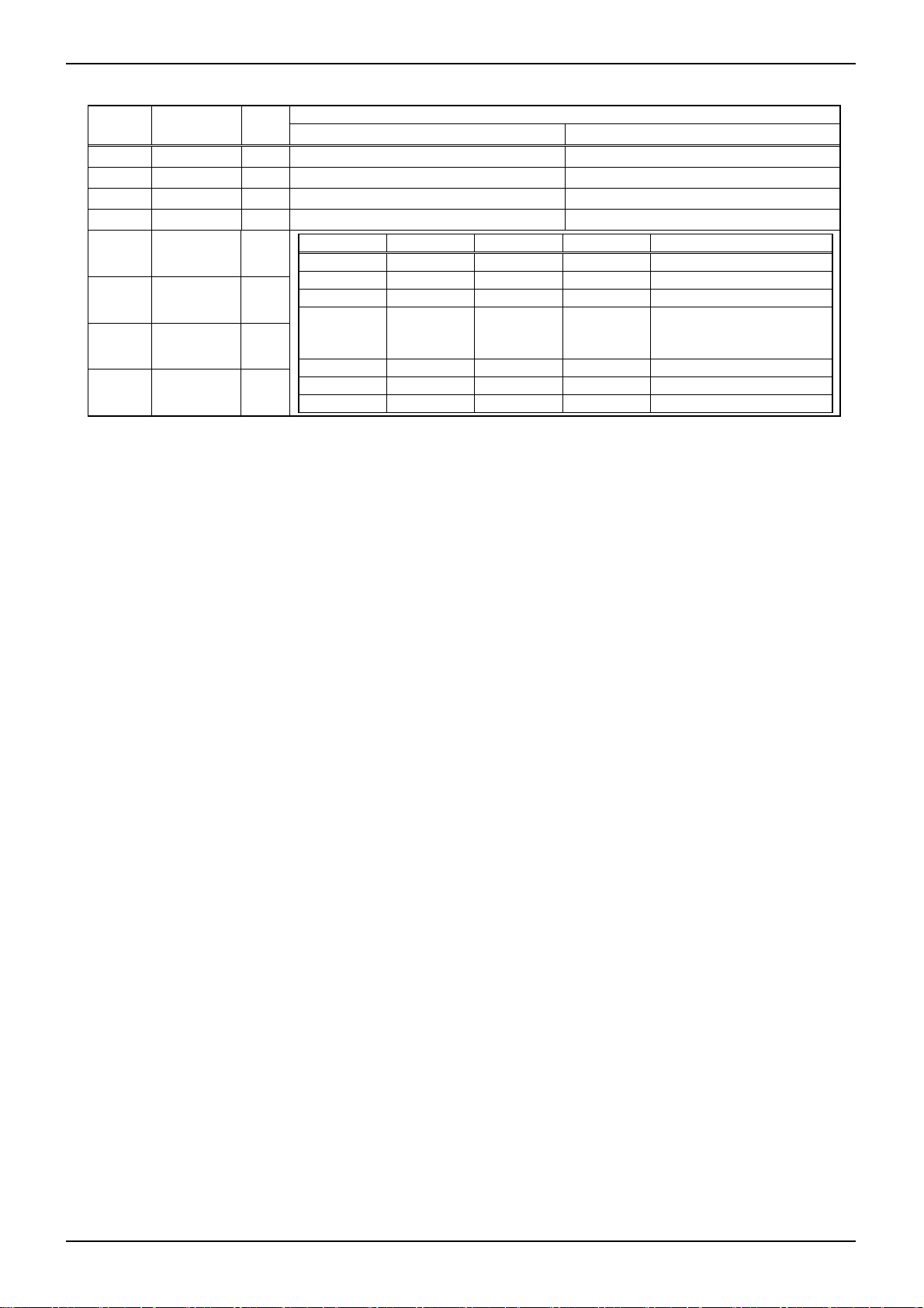
●Absolute Maximum Ratings(Ta=25℃)
2
C address change function and supporting reference clock I/O.
No.11041EAT12
Parameter Symbol Limits Unit
Maximum Applied voltage VMAX 7 V
Power Dissipation Pd 1250
Operating Temperature Range Topr -40 ~ +85 ℃
Storage Temperature Range Tstg -55 ~ +150 ℃
(Note1)Power dissipation deleting is 10.0mW/ oC, when it’s used in over 25 oC.
(It’s deleting is on the board that is ROHM’s standard)
●Recommended Operating Conditions(VBAT≧VIO, Ta=-40~85℃)
Parameter Symbol Limits Unit
VBAT input voltage VBAT 2.7 ~ 5.5 V
VIO pin voltage VIO 1.65 ~ 3.3 V
(Note1)
mW
www.rohm.com
© 2011 ROHM Co., Ltd. All rights reserved.
1/27
2011.04 - Rev.
Page 2

A
BD2802GU
●Electrical Characteristics(Unless otherwise specified, Ta=25℃, VBAT=3.6V, VIO=1.8V)
Parameter Symbol
【Circuit Current】
VBAT Circuit current 1 IBAT1 - 0.1 3.0 A RESETB=0V, VIO =0V
VBAT Circuit current 2 IBAT2 - 0.5 3.0 A RESETB=0V, VIO=1.8V
VBAT Circuit current 3 IBAT3 - 0.8 1.2 mA
【LED Driver】
LED current Step ILEDSTP 128 step RGB1 group, RGB2 group
Min. Typ. Max.
Limits
Unit Condition
LED 6Ch ON, ILED=10mA setting
Exclusive of LED current,
RGBISET =120k
Technical Note
LED Maximum setup
curren
LED current accurate ILED 18 20 22 mA
LED current Matching ILEDMT - 5 10 %
LED OFF Leak current ILKL - - 1.0 A
【OSC】
OSC oscillation frequency fosc 0.8 1.0 1.2 MHz
【SDA, SCL】(I2C interface )
L level input voltage VILI -0.3 - 0.25×VIO V
H level input voltage VIHI 0.75×VIO - VBAT+0.3 V
Hysteresis of Schmitt
trigger input
L level output voltage VOLI 0 - 0.3 V SDA pin, IOL=3 mA
Input current linI -10 - 10 A Input voltage = 0.1×VIO~0.9×VIO
【RESETB】(CMOS input pin)
L level input voltage VILR -0.3 - 0.25×VIO V
H level input voltage VIHR 0.75×VIO - VBAT+0.3 V
Input current IinR -10 - 10 A Input voltage = 0.1×VIO~0.9×VIO
【ADDSEL】(CMOS input pin)
L level input voltage VILADD -0.3 - 0.25×VBAT V
H level input voltage VIHADD 0.7 ×VBAT - VBAT+0.3 V
Input current IinADD -10 - 10 A Input voltage = 0.1×VBAT~0.9×VBAT
【RGB1CNT, RGB2CNT】(CMOS input pin with Pull-down resistance)
L level input voltage VILCNT -0.3 - 0.25×VIO V
H level input voltage VIHCNT 0.75×VIO - VBAT+0.3 V
Input current IinCNT - 3.6 10 A Input voltage = 1.8V
【CLKIO(Output)】(CMOS output pin)
L level output voltage VOLCLK - - 0.2 V IOL=1mA
H level output voltage VOHCLK VIO-0.2 - - V IOH=1mA
Output frequency fclk 200 250 300 kHz
【CLKIO (Input)】(CMOS input pin)
L level input voltage VILCLK -0.3 - 0.25×VIO V
H level input voltage VIHCLK 0.75×VIO - VIO+0.3 V
Input current IinCLK - 3.6 10 A Input voltage = 1.8V
IMAX - - 30.48 mA
VhysI 0.05×VIO - - V
RGB1 group, RGB2 group
RGBISET=100k
RGB1 group, RGB2 group,
Terminal voltage =1V
ILED=20mA setting, RGBISET
=120k
RGB1 group, between RGB2 group,
Terminal voltage =1V
ILED=20mA setting
www.rohm.com
© 2011 ROHM Co., Ltd. All rights reserved.
2/27
2011.04 - Rev.
Page 3
A
BD2802GU
A
A
A
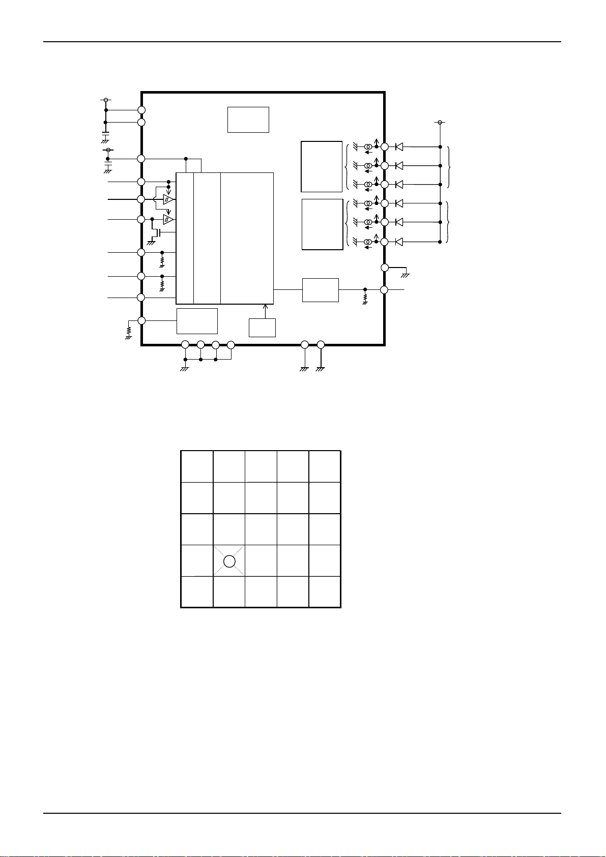
●Block Diagram / Application Circuit example
VBAT
VBAT2
VBAT1
1µF/10V
1µF/10V
RESETB
VIO
SCL
SD
I/O
Level
Shift
RGB1CNT
RGB2CNT
ADDSEL
RGBISET
IREF
T3
T1
T2
Fig.3 Block Diagram / Application Circuit example
●Pin Arrangement [Bottom View]
E
T4
G2LED
B2LED R2LED B1LED R1LED VBAT1
D
C
B
VBAT2
GND1
RGBISE
index
RGB2CNT
T1
1 2 3 4 5
VREF
I2C interface
Digital Control
TSD
T4
RGBGND
RGB1CNT
CLKIO SCL SDA
VIO RESETB
Slope
Control
(RGB1)
Slope
Control
(RGB2)
CLKIO
GND1
GND2
G1LED T3
DDSEL GND2
T2
R1LED
G1LED
B1LED
R2LED
G2LED
B2LED
RGBGND
CLKIO
VBAT
Technical Note
RGB1
RGB2
www.rohm.com
© 2011 ROHM Co., Ltd. All rights reserved.
3/27
2011.04 - Rev.
Page 4
A
BD2802GU
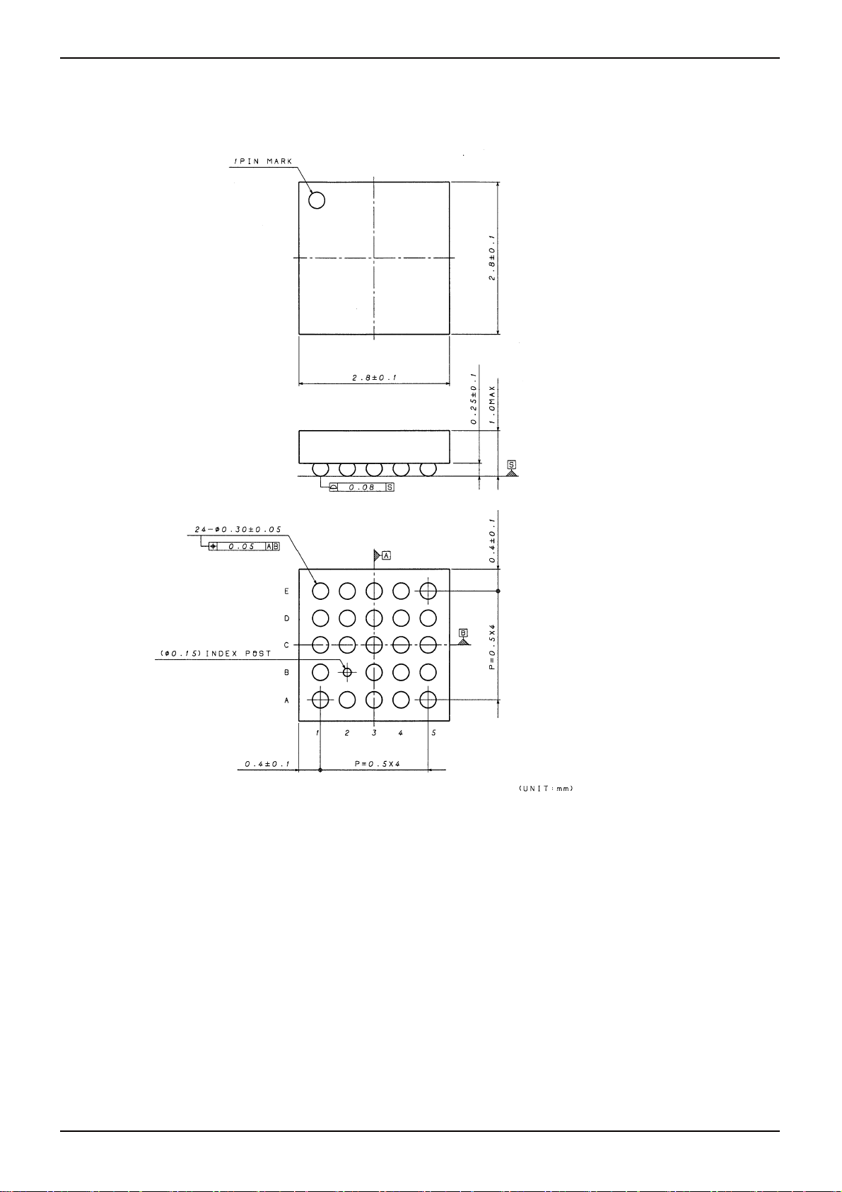
●Outside size figure
VCSP85H2 CSP small Package
Size : 2.8mm×2.8mm (Tolerance : ± 0.1mm each side) height 1.0mm max
Ball pitch : 0.5 mm
Technical Note
www.rohm.com
© 2011 ROHM Co., Ltd. All rights reserved.
4/27
2011.04 - Rev.
Page 5

A
BD2802GU
Technical Note
●Pin Functions
No Pin No. Pin Name I/O
Input Level
For Power For GND
ESD Diode Functions
1 D5 VBAT1 - - GND Battery is connected A
2 C1 VBAT2 - - GND Battery is connected A
3 A1 T1 - VBAT GND Test Pin (short to GND) S
4 A5 T2 - VBAT GND Test Pin (short to GND) S
5 E5 T3 - VBAT GND Test Pin (short to GND) S
6 E1 T4 - VBAT - Test Pin (short to GND) B
7 A3 VIO - VBAT GND I/O voltage source is connected C
8 A4 RESETB I VBAT GND Reset input (L: RESET, H: RESET cancel) H
9 B5 SDA I/O VBAT GND I2C data input I
10 B4 SCL I VBAT GND I2C clock input H
11 B1 GND1 - VBAT - Ground B
12 C5 GND2 - VBAT - Ground B
13 E3 RGBGND - VBAT - Ground B
14 C2 RGBISET I VBAT GND RGB LED reference current O
15 D4 R1LED I - GND Red LED1 connected E
16 E4 G1LED I - GND Green LED1 connected E
17 D3 B1LED I - GND Blue LED1 connected E
18 D2 R2LED I - GND Red LED2 connected E
19 E2 G2LED I - GND Green LED2 connected E
20 D1 B2LED I - GND Blue LED2 connected E
21 C3 RGB1CNT I VBAT GND
22 A2 RGB2CNT I VBAT GND
RGB1 LED external ON/OFF Synchronism
(L:OFF, H:ON)*
RGB2 LED external ON/OFF Synchronism
(L:OFF, H:ON)*
J
J
23 C4 ADDSEL I VBAT GND I2C device address change terminal R
24 B3 CLKIO I/O VBAT GND Standard clock input-and-output terminal V
* A setup of a register is separately necessary to validate it.
www.rohm.com
© 2011 ROHM Co., Ltd. All rights reserved.
5/27
2011.04 - Rev.
Page 6
A
BD2802GU
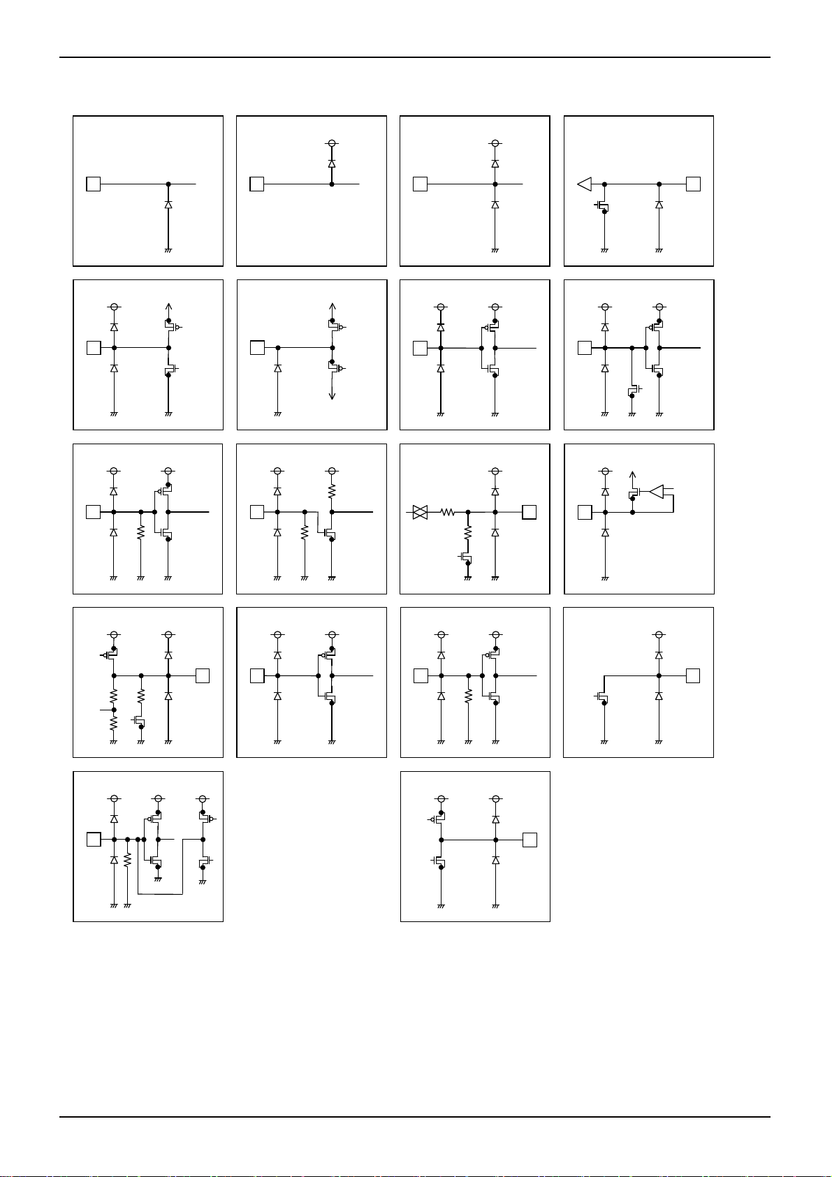
●Equivalent circuit diagram
A VBATB E
F G
VBAT
C
H
VBAT
VIOVBAT
Technical Note
I
VIO VBAT
J
Q
VBAT VBAT
VIO VBAT
R
VIO VBAT V
VIO
VBATVBAT L
VBATVBAT
N
S
X
VBAT VBAT
VBAT
VBATVBAT
O
VBAT
VBAT U
www.rohm.com
© 2011 ROHM Co., Ltd. All rights reserved.
6/27
2011.04 - Rev.
Page 7
A
BD2802GU
Technical Note
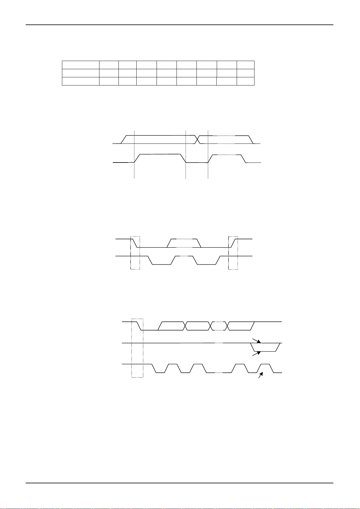
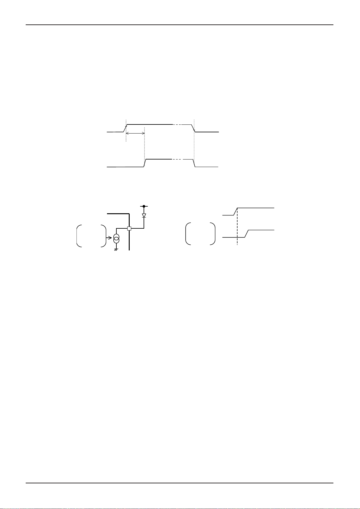
●I2C BUS format
The writing operation is based on the I2C slave standard.
・Slave address
A7 A6 A5 A4 A3 A2 A1 R/W
ADDSEL=L 0 0 1 1 0 1 0 0
ADDSEL=H 0 0 1 1 0 1 1 0
Slave address can be changed with the external terminal ADDSEL.
・Bit Transfer
SCL transfers 1-bit data during H. SCL cannot change signal of SDA during H at the time of bit transfer. If SDA changes
while SCL is H, START conditions or STOP conditions will occur and it will be interpreted as a control signal.
SDA
SCL
SDA a state of stability
Data are effective
SDA
:
It can change
・START and STOP condition
When SDA and SCL are H, data is not transferred on the I
2
C- bus. This condition indicates, if SDA changes from H to L
while SCL has been H, it will become START (S) conditions, and an access start, if SDA changes from L to H while SCL
has been H, it will become STOP (P) conditions and an access end.
SDA
SCL
S P
START condition
STOP condition
・Acknowledge
It transfers data 8 bits each after the occurrence of START condition. A transmitter opens SDA after transfer 8bits data, and
a receiver returns the acknowledge signal by setting SDA to L.
DATA OUTPUT
BY TRANSMITTER
DATA OUTPUT
BY RECEIVER
SCL
START condition
S
12 89
not acknowledge
acknowledge
clock pulse for
acknowledgement
www.rohm.com
© 2011 ROHM Co., Ltd. All rights reserved.
7/27
2011.04 - Rev.
Page 8
A
BD2802GU
AAA
A
A7 A6 A5 A4 A3 A2A1A
A
A
S
Technical Note
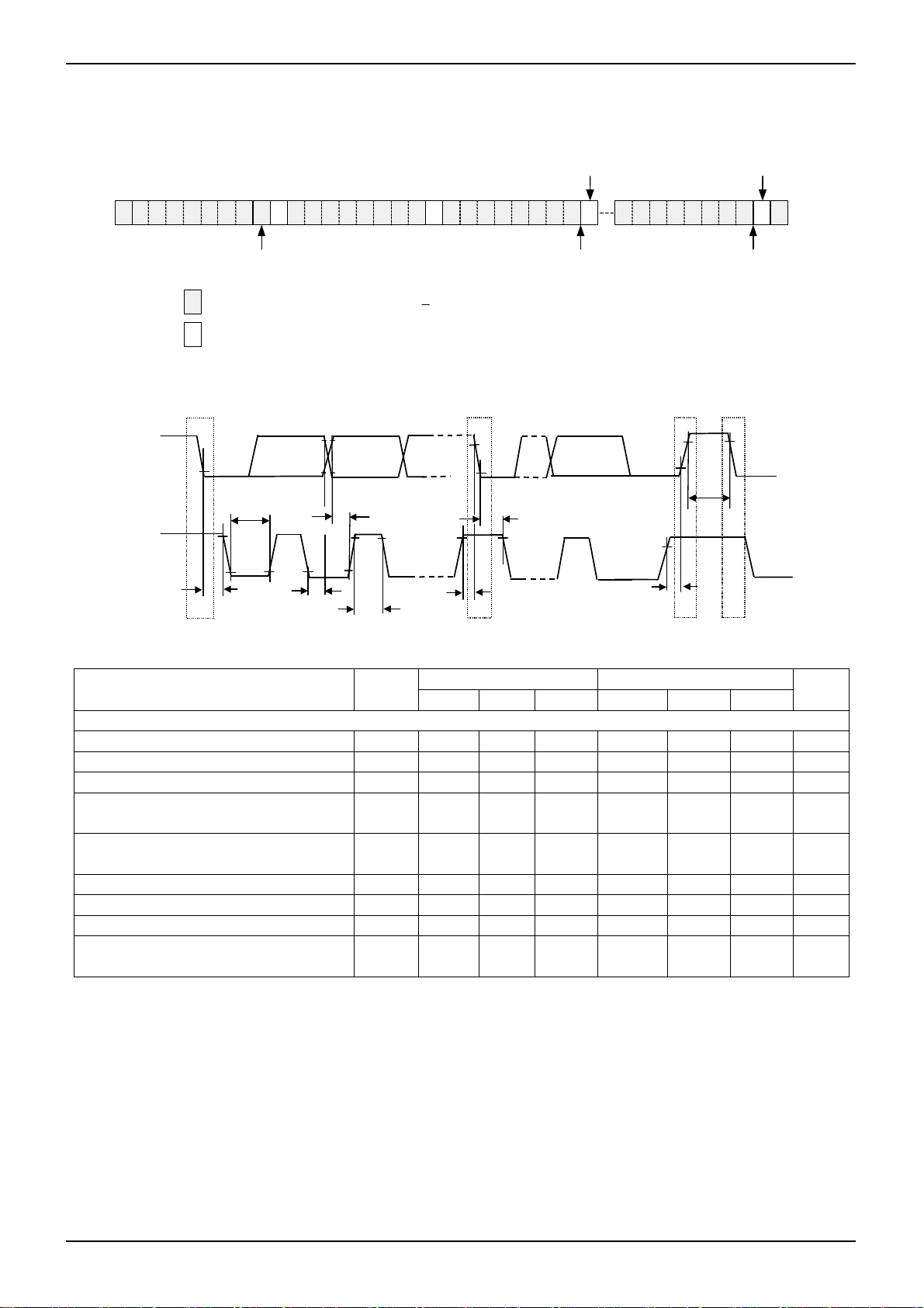
・Writing protocol
A register address is transferred by the next 1 byte that transferred the slave address and the write-in command. The 3rd
byte writes data in the internal register written in by the 2nd byte, and after 4th byte or, the increment of register address is
carried out automatically. However, when a register address turns into the last address, it is set to 00h by the next
transmission. After the transmission end, the increment of the address is carried out.
*1 *1
X X X X X X X
S
R/W=0(write)
from master to slave
from slave to master
register addressslave address
D7D6 D5 D4 D3 D2 D1 D0 D7D6 D5 D4 D3 D2 D1 D0
00
DATA
register address
increment
=acknowledge(SDA LOW)
=not acknowledge(SDA HIGH)
S=START condition
P=STOP condition
*1: Write Timing
DATA
register address
increment
P
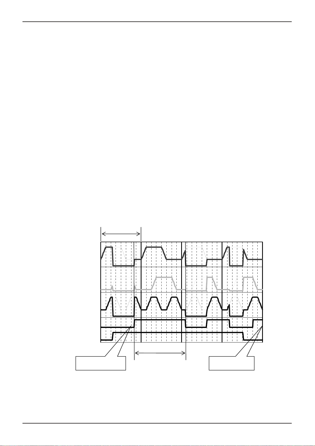
●Timing diagram
SDA
BUF
t
SU;DAT
t
t HIGH
CL
LOW
t
HD;STA
t
HD;DAT
S Sr P
t
●Electrical Characteristics(Unless otherwise specified, Ta=25
2
【I
C BUS format】
Parameter Symbol
Min. Typ. Max. Min. Typ. Max.
t
HD;STA
SU;STA
t
t SU;STO
S
o
C, VBAT=3.6V, VIO=1.8V)
Standard-mode Fast-mode
Unit
SCL clock frequency fSCL 0 - 100 0 - 400 kHz
LOW period of the SCL clock tLOW 4.7 - - 1.3 - - s
HIGH period of the SCL clock tHIGH 4.0 - - 0.6 - - s
Hold time (repeated) START condition
After this period, the first clock is generated
Set-up time for a repeated START
condition
tHD;STA 4.0 - - 0.6 - - s
SU;STA 4.7 - - 0.6 - - s
t
Data hold time tHD;DAT 0 - 3.45 0 - 0.9 s
Data set-up time tSU;DAT 250 - - 100 - - ns
Set-up time for STOP condition tSU;STO 4.0 - - 0.6 - - s
Bus free time between a STOP
and START condition
BUF 4.7 - - 1.3 - - s
t
www.rohm.com
© 2011 ROHM Co., Ltd. All rights reserved.
8/27
2011.04 - Rev.
Page 9

A
BD2802GU
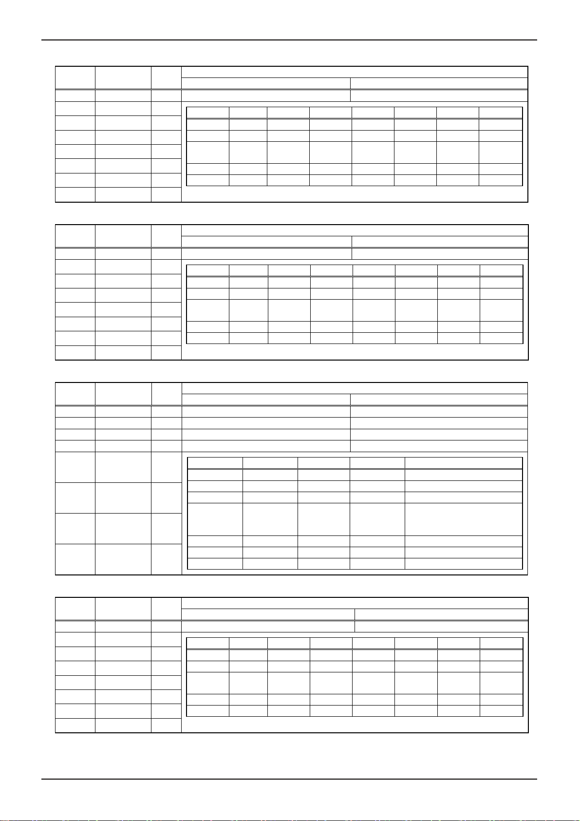
●Register map
Address W/R
Technical Note
Resister data
D7 D6 D5 D4 D3 D2 D1 D0
Function
00h W
01h W
02h W
03h W
04h W
05h W
06h W
07h W
08h W
09h W
0Ah W
0Bh W
0Ch W
0Dh W
0Eh W
- - CLKMD CLKEN - - - SFTRST
- RGB2MEL RGB2OS RGB2EN - RGB1MEL RGB1OS RGB1EN RBG-LED control
SFRGB1(1) SFRGB1(0) SRRGB1(1) SRRGB1(0) - TRGB1(2) TRGB1(1) TRGB1(0) RGB1-hour setup
- IR11(6) IR11(5) IR11(4) IR11(3) IR11(2) IR11(1) IR11(0) R1 current 1 setup
- IR12(6) IR12(5) IR12(4) IR12(3) IR12(2) IR12(1) IR12(0) R1 current 2 setup
- - - - PR1(3) PR1(2) PR1(1) PR1(0) R1 Wave patturn setup
- IG11(6) IG11(5) IG11(4) IG11(3) IG11(2) IG11(1) IG11(0) G1 current 1 setup
- IG12(6) IG12(5) IG12(4) IG12(3) IG12(2) IG12(1) IG12(0) G1 current 2 setup
- - - - PG1(3) PG1(2) PG1(1) PG1(0) G1 Wave patturn setup
- IB11(6) IB11(5) IB11(4) IB11(3) IB11(2) IB11(1) IB11(0) B1 current 1 setup
- IB12(6) IB12(5) IB12(4) IB12(3) IB12(2) IB12(1) IB12(0) B1 current 2 setup
- - - - PB1(3) PB1(2) PB1(1) PB1(0) B1 Wave patturn setup
SFRGB2(1) SFRGB2(0) SRRGB2(1) SRRGB2(0) - TRGB2(2) TRGB2(1) TRGB2(0) RGB2-hour setup
- IR21(6) IR21(5) IR21(4) IR21(3) IR21(2) IR21(1) IR21(0) R2 current 1 setup
- IR22(6) IR22(5) IR22(4) IR22(3) IR22(2) IR22(1) IR22(0) R2 current 2 setup
Soft Reset clock setup
0Fh W
10h W
11h W
12h W
13h W
14h W
15h W
- - - - PR2(3) PR2(2) PR2(1) PR2(0) R2 Wave patturn
- IG21(6) IG21(5) IG21(4) IG21(3) IG21(2) IG21(1) IG21(0) G2 current 1 setup
- IG22(6) IG22(5) IG22(4) IG22(3) IG22(2) IG22(1) IG22(0) G2 current 2 setup
- - - - PG2(3) PG2(2) PG2(1) PG2(0) G2 Wave patturn setup
- IB21(6) IB21(5) IB21(4) IB21(3) IB21(2) IB21(1) IB21(0) B2 current 1 setup
- IB22(6) IB22(5) IB22(4) IB22(3) IB22(2) IB22(1) IB22(0) B2 current 2 setup
- - - - PB2(3) PB2(2) PB2(1) PB2(0) B2 Wave patturn setup
Input "0” for "-".
Vacancy address may be use for test.
Prohibit to accessing the address that isn’t mentioned and the register for test.
www.rohm.com
© 2011 ROHM Co., Ltd. All rights reserved.
9/27
2011.04 - Rev.
Page 10

A
BD2802GU
●Register Description
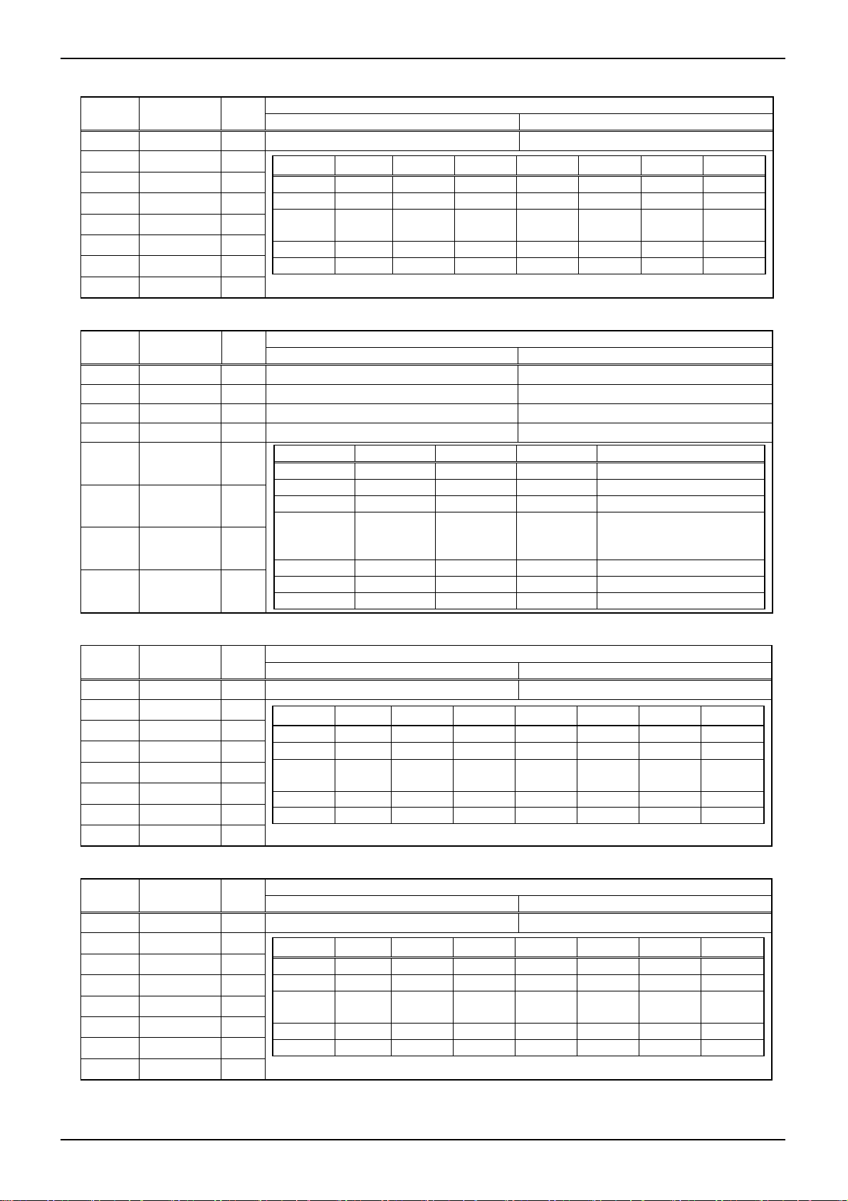
Adress 00h <Soft Reset>
BIT Name Initial
0 1
Function
D7 - - - D6 - - - D5 CLKMD 0 Clock Input mode Clock Output mode
D4 CLKEN 0 Clock input and output invalid Clock input and output Effective
D3 - - - -
D2 - - - -
D1 - - - -
D0 SFTRST 0 Reset Release Reset
Adress 01h <RGB LED control >
BIT Name Init
0 1
Function
D7 - - - -
D6 RGB2MEL 0 RGB2 external control invalid RGB2 external control valid
D5 RGB2OS 0 RGB2 Stop RGB2 1 periodic operation
D4 RGB2EN 0 RGB2 Stop RGB2 continuous operation
D3 - - - -
D2 RGB1MEL 0 RGB1 external control invalid RGB1 external control valid
D1 RGB1OS 0 RGB1 Stop RGB1 1 periodic operation
D0 RGB1EN 0 RGB1 Stop RGB1 continuous operation
* RGB*OS returns to 0 automatically after 1 cycle operation.
* RGB*EN precedes to RGB*OS. In use in 1 cycle operation, there is the necessity for RGB*EN=0.
Adress 02h <RGB1 time>
BIT Name Init
0 1
Function
Technical Note
SFRGB1(1) SFRGB1(0) Slope Down transition
D7 SFRGB1(1) 0
0 0 0
0 1 Wave form cycle / 16
1 0 Wave form cycle / 8
1 1 Wave form cycle / 4
D6 SFRGB1(0) 0
It is a theoretical value on logic control, and the reaction time of the analog section is
not included."Slope time" is the time from a slope start to a slope end.
SRRGB1(1) SRRGB1(0) Slope Up transition
D5 SRRGB1(1) 0
0 0 0
0 1 Wave form cycle / 16
1 0 Wave form cycle / 8
1 1 Wave form cycle / 4
D4 SRRGB1(0) 0
It is a theoretical value on logic control, and the reaction time of the analog section is not
included."Slope time" is the time from a slope start to a slope end.
D3 - - - -
D2 TRGB1(2) 0
TRGB1(2) TRGB1(1) TRGB1(0) Wave form cycle
0 0 0 0.131 s
0 0 1 0.52 s
0 1 0 1.05 s
D1 TRGB1(1) 0
0 1 1 2.10 s
1 0 0 4.19 s
1 0 1 8.39 s
D0 TRGB1(0) 0
1 1 0 12.6 s
1 1 1 16.8 s
Setting time is counted based on the frequency of OSC. The above-mentioned value is a value at the time of Typ (1MHz).
When operating by the external clock, input frequency is a value at the time of Typ (250kHz).
*Refer to "●Use of a RGB wave setup " for the detailed function of each register of this page.
www.rohm.com
© 2011 ROHM Co., Ltd. All rights reserved.
10/27
2011.04 - Rev.
Page 11
A
BD2802GU
Adress 03h <R1 current 1setup >
BIT Name Init
0 1
Function
D7 - - - -
D6 IR11(6) 0
D5 IR11(5) 0
D4 IR11(4) 0
D3 IR11(3) 0
D2 IR11(2) 0
D1 IR11(1) 0
D0 IR11(0) 0
IR11(6) IR11(5) IR11(4) IR11(3) IR11(2) IR11(1) IR11(0) Current
0 0 0 0 0 0 0 0
0 0 0 0 0 0 1 0.2mA
・
・
・
・
・
・
・
・
・
・
・
・
1 1 1 1 1 1 0 25.2mA
1 1 1 1 1 1 1 25.4mA
At RGBISETpin 120k connection
Adress 04h <R1 current2 setup >
BIT Name Init
0 1
Function
D7 - - - -
D6 IR12(6) 0
D5 IR12(5) 0
D4 IR12(4) 0
D3 IR12(3) 0
D2 IR12(2) 0
D1 IR12(1) 0
D0 IR12(0) 0
IR12(6) IR12(5) IR12(4) IR12(3) IR12(2) IR12(1) IR12(0) Current
0 0 0 0 0 0 0 0
0 0 0 0 0 0 1 0.2mA
・
・
・
・
・
・
・
・
・
・
・
・
1 1 1 1 1 1 0 25.2mA
1 1 1 1 1 1 1 25.4mA
At RGBISETpin 120k connection
Adress 05h <R1 Wave Pattern >
BIT Name Init
0 1
Function
D7 - - - -
D6 - - - -
D5 - - - -
D4 - - - -
Technical Note
・
・
・
・
0.2mA
step
0.2mA
step
D3
PR1(3) 0
PR1(3) PR1(2) PR1(1) PR1(0) Wave
0 0 0 0 Pattern1
0 0 0 1 Pattern2
D2 PR1(2) 1
D1 PR1(1) 1
0 0 1 0 Pattern3
・
・
・
・
・
・
・
・
・
・
・
・
1 1 0 1 Pattern14
D0 PR1(0) 1
1 1 1 0 Pattern15
1 1 1 1 Pattern16
Adress 06h <G1 current1 setup >
BIT Name Init
0 1
Function
D7 - - - -
D6 IG11(6) 0
D5 IG11(5) 0
D4 IG11(4) 0
D3 IG11(3) 0
D2 IG11(2) 0
D1 IG11(1) 0
D0 IG11(0) 0
IG11(6) IG11(5) IG11(4) IG11(3) IG11(2) IG11(1) IG11(0) Current
0 0 0 0 0 0 0 0
0 0 0 0 0 0 1 0.2mA
・
・
・
・
・
・
・
・
・
・
・
・
1 1 1 1 1 1 0 25.2mA
1 1 1 1 1 1 1 25.4mA
At RGBISETpin 120k connection
*Refer to "●Use of a RGB wave setup " for the detailed function of each register of this page.
・
・
・
・
・
0.2mA
step
www.rohm.com
© 2011 ROHM Co., Ltd. All rights reserved.
11/27
2011.04 - Rev.
Page 12

A
BD2802GU
Adress 07h <G1 current2 setup >
BIT Name Init
0 1
Function
D7 - - - -
D6
D5 IG12(5) 0
D4 IG12(4) 0
D3 IG12(3) 0
D2 IG12(2) 0
D1 IG12(1) 0
D0 IG12(0) 0
IG12(6) 0
IG12(6) IG12(5) IG12(4) IG12(3) IG12(2) IG12(1) IG12(0) Current
0 0 0 0 0 0 0 0
0 0 0 0 0 0 1 0.2mA
・
・
・
・
・
・
・
・
・
・
・
・
1 1 1 1 1 1 0 25.2mA
1 1 1 1 1 1 1 25.4mA
At RGBISETpin 120k connection
Adress 08h <G1 G1 Wave Pattern >
BIT Name Init
0 1
Function
D7 - - - D6 - - - D5 - - - D4 - - - -
D3
PG1(3) 0
PG1(3) PG1(2) PG1(1) PG1(0) Wave
0 0 0 0 Pattern 1
0 0 0 1 Pattern 2
D2 PG1(2) 1
D1 PG1(1) 1
0 0 1 0 Pattern 3
・
・
・
・
・
・
・
・
・
・
・
・
1 1 0 1 Pattern 14
D0 PG1(0) 1
1 1 1 0 Pattern 15
1 1 1 1 Pattern 16
Adress 09h <B1 current1setup >
BIT Name Init
0 1
Function
D7 - - - -
D6
D5 IB11(5) 0
D4 IB11(4) 0
D3 IB11(3) 0
D2 IB11(2) 0
D1 IB11(1) 0
D0 IB11(0) 0
IB11(6) 0
At RGBISETpin 120k connection
IB11(6) IB11(5) IB11(4) IB11(3) IB11(2) IB11(1) IB11(0) Current
0 0 0 0 0 0 0 0
0 0 0 0 0 0 1 0.2mA
・
・
・
・
・
・
・
・
・
・
・
・
1 1 1 1 1 1 0 25.2mA
1 1 1 1 1 1 1 25.4mA
Adress 0Ah <B1 current2setup >
BIT Name Init
0 1
Function
D7 - - - D6
D5 IB12(5) 0
D4 IB12(4) 0
D3 IB12(3) 0
D2 IB12(2) 0
D1 IB12(1) 0
D0 IB12(0) 0
IB12(6) 0
IB12(6) IB12(5) IB12(4) IB12(3) IB12(2) IB12(1) IB12(0) Current
0 0 0 0 0 0 0 0
0 0 0 0 0 0 1 0.2mA
・
・
・
・
・
・
・
・
・
・
・
・
1 1 1 1 1 1 0 25.2mA
1 1 1 1 1 1 1 25.4mA
At RGBISETpin 120k connection
*Refer to "●Use of a RGB wave setup " for the detailed function of each register of this page.
Technical Note
・
・
・
・
・
・
0.2mA
step
・
・
・
0.2mA
step
0.2mA
step
www.rohm.com
© 2011 ROHM Co., Ltd. All rights reserved.
12/27
2011.04 - Rev.
Page 13

A
BD2802GU
Adress 0Bh <B1 Wave Pattern >
BIT Name Init
0 1
Function
D7 - - - D6 - - - D5 - - - D4 - - - -
Technical Note
D3
PB1(3) 0
D2 PB1(2) 1
D1 PB1(1) 1
D0 PB1(0) 1
Adress 0Ch <RGB2 time >
BIT Name Init
D7 SFRGB2(1) 0
D6 SFRGB2(0) 0
D5 SRRGB2(1) 0
D4 SRRGB2(0) 0
PB1(3) PB1(2) PB1(1) PB1(0) Wave
0 0 0 0 Pattern1
0 0 0 1 Pattern2
0 0 1 0 Pattern3
・
・
・
・
・
・
・
・
・
・
・
・
・
・
・
1 1 0 1 Pattern14
1 1 1 0 Pattern15
1 1 1 1 Pattern16
Function
0 1
SFRGB2(1) SFRGB2(0) Slope Down transition
0 0 0
0 1 Wave form cycle / 16
1 0 Wave form cycle / 8
1 1 Wave form cycle / 4
It is a theoretical value on logic control, and the reaction time of the analog section is
not included.
"Slope time" is the time from a slope start to a slope end.
SRRGB2(1) SRRGB2(0) Slope up transition
0 0 0
0 1 Wave form cycle / 16
1 0 Wave form cycle / 8
1 1 Wave form cycle / 4
It is a theoretical value on logic control, and the reaction time of the analog section is not
included.
"Slope time" is the time from a slope start to a slope end.
D3 - - - -
TRGB2(2) TRGB2(1) TRGB2(0) Wave form cycle
D2 TRGB2(2) 0
0 0 0 0.131 s
0 0 1 0.52 s
0 1 0 1.05 s
D1 TRGB2(1) 0
0 1 1 2.10 s
1 0 0 4.19 s
1 0 1 8.39 s
D0 TRGB2(0) 0
1 1 0 12.6 s
1 1 1 16.8 s
Setting time is counted based on the frequency of OSC. The above-mentioned value is a value at the time of Typ (1MHz).
When operating by the external clock, input frequency is a value at the time of Typ (250kHz)
*Refer to "●Use of a RGB wave setup " for the detailed function of each register of this page.
www.rohm.com
© 2011 ROHM Co., Ltd. All rights reserved.
13/27
2011.04 - Rev.
Page 14

A
BD2802GU
Adress 0Dh <R2 current 1setup>
BIT
D7
D6
Name Init
- - - -
IR21(6) 0
D5 IR21(5) 0
D4 IR21(4) 0
D3 IR21(3) 0
D2 IR21(2) 0
D1 IR21(1) 0
D0 IR21(0) 0
At RGBISETpin 120k connection
0 1
IR21(6) IR21(5) IR21(4) IR21(3) IR21(2) IR21(1) IR21(0)
0 0 0 0 0 0 0 0
0 0 0 0 0 0 1 0.2mA
・
・
・
・
・
・
1 1 1 1 1 1 0 25.2mA
1 1 1 1 1 1 1 25.4mA
Function
・
・
・
・
・
・
Adress 0Eh <R2 current 2setup>
BIT Name Init
0 1
Function
D7 - - - D6
D5 IR22(5) 0
D4 IR22(4) 0
D3 IR22(3) 0
D2 IR22(2) 0
D1 IR22(1) 0
D0 IR22(0) 0
IR22(6) 0
IR22(6) IR22(5) IR22(4) IR22(3) IR22(2) IR22(1) IR22(0)
0 0 0 0 0 0 0 0
0 0 0 0 0 0 1 0.2mA
・
・
・
・
・
・
・
・
・
・
・
・
1 1 1 1 1 1 0 25.2mA
1 1 1 1 1 1 1 25.4mA
At RGBISETpin 120k connection
Adress 0Fh <R2 Wave Pattern setup>
BIT Name Init
0 1
Function
D7 - - - D6 - - - D5 - - - D4 - - - -
D3
PR2(3) 0
PR2(3) PR2(2) PR2(1) PR2(0) Wave
0 0 0 0 Pattern 1
0 0 0 1 Pattern 2
D2 PR2(2) 1
D1 PR2(1) 1
0 0 1 0 Pattern 3
・
・
・
・
・
・
・
・
・
・
・
・
1 1 0 1 Pattern 14
D0 PR2(0) 1
1 1 1 0 Pattern 15
1 1 1 1 Pattern 16
Adress 10h <G2 current 1setup>
BIT Name Init
D7 - -
D6
IG21(6) 0
IG21(6) IG21(5) IG21(4) IG21(3) IG21(2) IG21(1) IG21(0)
D5 IG21(5) 0
D4 IG21(4) 0
D3 IG21(3) 0
D2 IG21(2) 0
D1 IG21(1) 0
D0 IG21(0) 0
At RGBISETpin 120k connection
0 1
- -
0 0 0 0 0 0 0 0
0 0 0 0 0 0 1 0.2mA
・
・
・
・
・
・
1 1 1 1 1 1 0 25.2mA
1 1 1 1 1 1 1 25.4mA
Function
・
・
・
・
・
・
*Refer to "●Use of a RGB wave setup " for the detailed function of each register of this page.
Technical Note
Current
・
・
・
・
・
・
0.2mA
step
Current
0.2mA
step
・
・
・
Current
0.2mA
step
www.rohm.com
© 2011 ROHM Co., Ltd. All rights reserved.
14/27
2011.04 - Rev.
Page 15
A
BD2802GU
Adress 11h <G2 current 2setup>
BIT Name Init
D7 - -
D6
IG22(6) 0
IG22(6) IG22(5) IG22(4) IG22(3) IG22(2) IG22(1) IG22(0)
D5 IG22(5) 0
D4 IG22(4) 0
D3 IG22(3) 0
D2 IG22(2) 0
D1 IG22(1) 0
D0 IG22(0) 0
At RGBISETpin 120k connection
0 1
- -
0 0 0 0 0 0 0 0
0 0 0 0 0 0 1 0.2mA
・
・
・
・
・
・
1 1 1 1 1 1 0 25.2mA
1 1 1 1 1 1 1 25.4mA
Function
・
・
・
・
Adress 12h <G2 Wave Pattern setup >
BIT Name Init
D7 - -
D6 - -
D5 - -
D4 - -
D3
PG2(3) 0
0 1
- -
-
-
-
PG2(3) PG2(2) PG2(1) PG2(0) Wave
0 0 0 0 Pattern 1
Function
0 0 0 1 Pattern 2
D2 PG2(2) 1
D1 PG2(1) 1
0 0 1 0 Pattern 3
・
・
・
・
・
・
・
・
・
・
・
・
1 1 0 1 Pattern 14
D0 PG2(0) 1
1 1 1 0 Pattern 15
1 1 1 1 Pattern 16
Adress 13h <B2 current 1setup>
BIT Name Init
D7 - -
D6 IB21(6) 0
IB21(6) IB21(5) IB21(4) IB21(3) IB21(2) IB21(1) IB21(0)
D5 IB21(5) 0
D4 IB21(4) 0
D3 IB21(3) 0
D2 IB21(2) 0
D1 IB21(1) 0
D0 IB21(0) 0
At RGBISETpin 120k connection
0 1
- -
0 0 0 0 0 0 0 0
0 0 0 0 0 0 1 0.2mA
・
・
・
・
・
・
1 1 1 1 1 1 0 25.2mA
1 1 1 1 1 1 1 25.4mA
Function
・
・
・
・
Adress 14h <B2 current 2setup>
BIT
Name Init
D7 - -
D6
IB22(6) 0
IB22(6) IB22(5) IB22(4) IB22(3) IB22(2) IB22(1) IB22(0)
D5 IB22(5) 0
D4 IB22(4) 0
D3 IB22(3) 0
D2 IB22(2) 0
D1 IB22(1) 0
D0 IB22(0) 0
At RGBISETpin 120k connection
0 1
- -
0 0 0 0 0 0 0 0
0 0 0 0 0 0 1 0.2mA
・
・
・
・
・
・
1 1 1 1 1 1 0 25.2mA
1 1 1 1 1 1 1 25.4mA
Function
・
・
・
・
*Refer to "●Use of a RGB wave setup " for the detailed function of each register of this page.
・
・
・
・
・
・
Technical Note
Current
・
・
-
-
-
・
・
・
・
0.2mA
・
・
・
Current
0.2mA
Current
0.2mA
step
step
step
www.rohm.com
© 2011 ROHM Co., Ltd. All rights reserved.
15/27
2011.04 - Rev.
Page 16
A
BD2802GU
Adress 15h <B2 Wave Pattern setup >
BIT Name Init
D7 - -
D6 - -
D5 - -
D4 - -
D3
PB2(3) 0
0
-
-
-
-
PB2(3) PB2(2) PB2(1) PB2(0) Wave
0 0 0 0 Pattern 1
Function
0 0 0 1 Pattern 2
D2 PB2(2) 1
D1 PB2(1) 1
0 0 1 0 Pattern 3
・
・
・
・
・
・
・
・
・
・
・
・
1 1 0 1 Pattern 14
D0 PB2(0) 1
1 1 1 0 Pattern 15
1 1 1 1 Pattern 16
*Refer to "●Use of a RGB wave setup " for the detailed function of each register of this page.
Technical Note
1
-
-
-
-
・
・
・
www.rohm.com
© 2011 ROHM Co., Ltd. All rights reserved.
16/27
2011.04 - Rev.
Page 17
A
BD2802GU
Technical Note
RGB LED Driver Operation Description
- Two drivers “RGB1 (R1LED, G1LED, B1LED)” and “RGB2 (R2LED, G2LED, B2LED)” are mounted.
- A slope function is incorporated to control drivers independently.
- Refer to
RGB Waveform Setting for more information about output waveform setting.
- The LED current can be set via a resistance value (RISET) to be connected to the RGBISET terminal. The maximum
current value can be derived from the following expression:
ILEDmax [A] = 3.048 / RISET [k] (Typ)
However, this setting must be made so that the maximum current value can be less than or equal to 30.48mA. In
addition, the RGBISET terminal has an overcurrent protection circuit to prevent the excessive LED current from flowing
for low impedance to the ground.
- Note that the setting voltage shall be higher than or equal to a saturation voltage (0.2V) in the constant current circuit.
When LED Vf is large, the LED destination shall be connected to another step-up circuit.
RGB*EN
または
RGB*EN
RGB*OS
or
RFB*OS
T
on
(Max:20ms)
LED電流
LED current
- The LED destination is fixed before on (RGB*EN=Hi or RGB*OS=Hi).
VLED
VLED
RGB*EN
Or
RGB*OS
RGB*EN
Or
RGB*OS
●The synchronism of RGB1/RGB2
The period of RGB1 and RGB2 and start, stop timing can be set up independently.
When synchronizes RGB1 and RGB2, You must start an internal counter at the same time under the state of resetting.
(Internal Counter are prepared for each of RGB1 and RGB2, so You must reset both.)
<How to reset internal Counter>
Inside Counter can be reset by carrying out one of following actions.
• Reset by hard reset (RSTB_IL). (RGB1, RGB2 is reset together.)
• Reset by soft reset. (RGB1, RGB2 is reset together.)
• It is written register of the current setup (I1
・I2), the slope setup, the period setup and the pattern setup.
Internal Counter of RGB1 is reset when it is written between Address=0Bh from 02h.
Internal Counter of RGB2 is reset when it is written between Address=15h from 0Ch.
Counter is reset as to overwriting the same value.
Note)
Internal Counter isn't reset if write RGB1EN =L and RGB2EN =L. (Address=01h).
When it write RGB1EN=L (RGB2EN=L), inside Counter is held, and IC will operate from the held state at next restart.
www.rohm.com
© 2011 ROHM Co., Ltd. All rights reserved.
17/27
2011.04 - Rev.
Page 18
A
BD2802GU
A
Technical Note
●RGB Waveform Setting
Various kinds of RGB control can be implemented by designating waveform cycles, waveform patterns, current settings 1, 2
and rising/falling slope times.
To activate a RGB waveform, a continuous operation via RGB*EN or a single-shot operation via RGB*OS can be selected.
In addition, when control via the external terminal RGB*CNT is enabled via RGB*MEL, the corresponding LED can be lit in
synchronization with the external signal.
1. Waveform cycle
A single cycle time is set for a waveform pattern.
This setting can be made independently for RGB1 and RGB2.
2. Waveform pattern
A pattern in a waveform cycle is set.
Sixteen types of waveform patterns can be set in units of waveform patterns.
For concrete waveform patterns, refer to the timing diagram shown on the next page.
3. Current settings 1 and 2 (I1, I2)
Two currents in a waveform pattern are set.
When the maximum current value is 25.4mA, it is possible to set the current ranging from 0 to 25.4mA with an
increment of 0.2mA (128 steps).
The polarity of a waveform is determined by the greater-than/ less-than relationship in the current setting.
This setting can be made in units of terminals.
4. Rising/falling slope time
A current change time during switching between current settings 1 and 2 is set.
A time per step (0.2mA) is calculated based on a difference between the currents selected in current settings 1, 2
and a setting slope time.
For this reason, a time per step (0.2mA) is short when a difference between setting currents I1 and I2 is large. In
contrast, it is long when a difference between setting currents I1 and I2 is small.
Regardless of current settings 1 and 2, a rising slope time applies at current increase and a falling slope time applies
at current decrease. For concrete waveform images, refer to the timing diagram shown on the next page.
5. External terminal synchronization control
When control via the external terminal RGB*CNT is enabled via RGB*MEL, lighting is enabled if the input external signal
goes “H.” In contrast, it is disabled if the external input signal goes “L.” In this way, synchronization with the external
signal is enabled so that LED can be blinked in conjunction with a ringing tone (a melody signaling a ringtone).
Waveform cycle
RGB thin line indicates an image where
external terminal control does not take
place.
R*LED
G*LED
B*LED
RGB*CNT
RGB*MEL
External terminal control
is enabled.
Remains “Enabled” with
RGB*MEL=1 and
RGB*CNT=H
External terminal
control is disabled.
www.rohm.com
© 2011 ROHM Co., Ltd. All rights reserved.
18/27
2011.04 - Rev.
Page 19
A
BD2802GU
Wave pattern
Wave pattern
Wave pattern
Wave pattern
Wave pattern
Wave pattern
Wave pattern
Wave pattern
Wave pattern
Wave pattern
Wave pattern
Wave pattern
Wave pattern
Wave pattern
Wave pattern
Wave pattern
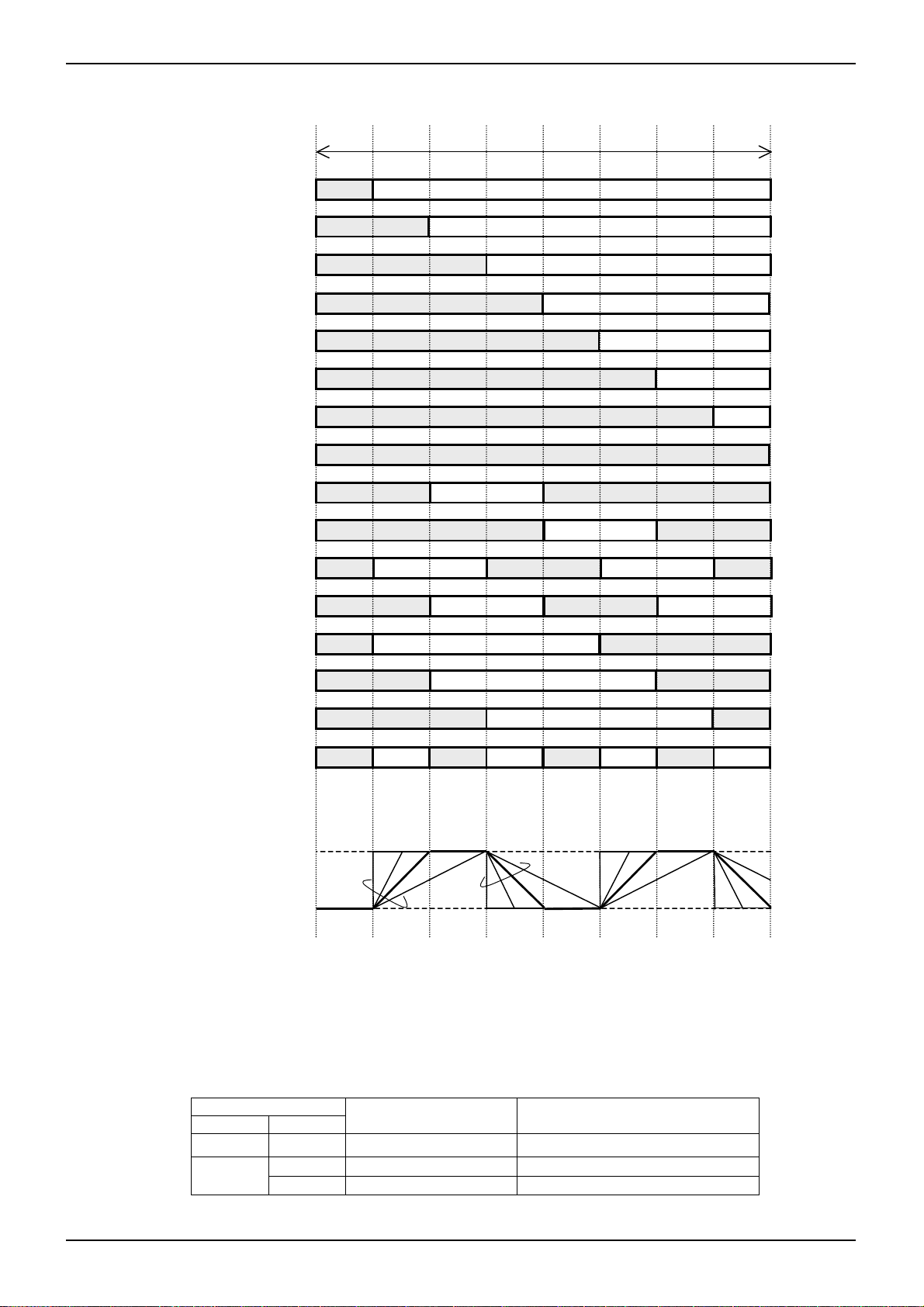
6. Clock I/O
A reference clock I/O function is mounted in this IC chip. When two IC chips are used to extend an illumination
capability, clock supply to the other RGB LED driver can be accomplished for synchronization with this LSI chip.
This setting can be made via the register.
Clock output can be made with CLKEN=1 and CLKMD=1.
Wave cycle
Register data
1 (00h)
2 (01h)
3 (02h)
4 (03h)
5 (04h)
6 (05h)
7 (06h)
8 (07h)
9 (08h)
10 (09h)
11 (0Ah)
12 (0Bh)
13 (0Ch)
14 (0Dh)
15 (0Eh)
16 (0Fh)
(ex)
The image of current change of Wave pattern 11
I1 I2
I1 I2
I1 I2
I1 I2
I1 I2
I1 I2
I1 I2
I1
I1 I2 I1
I1 I2 I1
I1 I2 I1 I2 I1
I1 I2 I1 I2
I1
I1
I1
I2
I2
I2
I1 I1I2 I2 I1 I1 I2 I2
Slope Down transition
Current 2(I2)
Slope uptransition
Current 1(I1)
RGB wave setting timing diagram
Register
CLKEN CLKMD
0 0/1 Input Does not receive external clocks.
1
0 Input Operates on external clocks.
1 Output -
CLKIO terminal state Clock reception
Technical Note
I1
I1
I1
www.rohm.com
© 2011 ROHM Co., Ltd. All rights reserved.
19/27
2011.04 - Rev.
Page 20

A
BD2802GU
●When two BD2802GU drivers are used and the clock is shared by CLKIO:
Because a sequence is already programmed within an IC chip for RGB falling, “Enable” shall be set to “OFF” and
clock supply shall be continued for at least three clocks so that operations can be performed using external clocks.
*Even in independent slave mode, its setting “Enable” shall be reset to “OFF” and then clock supply must be
continued for 3 clocks or more.
Clock I/O switching shall be avoided during RGB operation.
Enable: CLKEN, RGB1EN, RGB2EN, RGB1OS, RGB2OS
- Setting example
マスター側
スレーブ側
Enable
Master enabled
Slave enabled
Enable
(min=0ms)
min=
スレーブ側入力クロックの3クロック分
min = slave input clock (3 clocks)
(
マスター側のクロックを使用している場合は
(For master clocks in use: min = 15 s)
Master: Chip using CLKIO as output
Slave: Chip using CLKIO as input
Master side (clock output side) RGB waveform setting
Slave side (clock input side) RGB waveform setting
Master side Clock output setting
CLKEN=1, CLKMD=1 … Performs clock output.
Slave side Clock input setting
CLKEN=1, CLKMD=0 … Allows clock reception.
Master side RGB lighting
This duration shall be short as much as possible.
Slave side RGB lighting
min=15μs)
Technical Note
www.rohm.com
© 2011 ROHM Co., Ltd. All rights reserved.
20/27
2011.04 - Rev.
Page 21
A
BD2802GU
g
y
y
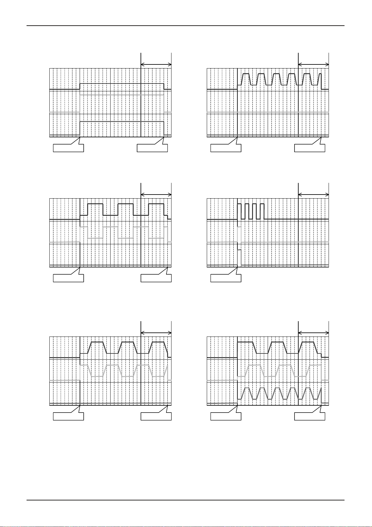
7. RGB waveform setting examples
[Example 1] Normal operation
動作
波形周期【例1】ノーマル
Waveform cycle
16Hz動作
[Example 4] 16Hz operation
Technical Note
波形周期【例4】
Waveform cycle
R*LED
G*LED
B*LED
Selecting a waveform pattern 8 causes a continuous
normal operation to take place through the setting
current 1.
[Example 2] Blinking
R*LED
G*LED
B*LED
RGB*EN=1 RGB*EN=0
波形周期【例2】ブリンク動作
Waveform cycle
R*LED
G*LED
B*LED
RGB*EN=1 RGB*EN=0
Combining the settings of a waveform pattern 11 and a
waveform cycle 131ms causes blinking at a rate of
15.3Hz (approx. 16Hz).
[Example 5] Continuous lighting of four
R*LED
G*LED
B*LED
LEDs
波形周期【例5】4連単発
Waveform cycle
RGB*EN=1 RGB*EN=0
Setting a rising/falling slope time to “0” causes blinking
to take place. Phase switching takes place via the
currents of R and G.
settin
[Example 3] Slope operation
R*LED
G*LED
B*LED
RGB*EN=1 RGB*EN=
When a rising/falling slope time is longer than the
setting made in example 2, a continuous color change
is made b
動作
slope operation.
波形周期【例3】スロープ
Waveform cycle
0
RGB*OS=1
This example shows that lighting occurs continuously in
the order of white, red, red and red. To achieve this,
waveform patterns 16, 1 and RGB*OS single cycle
operation need to be combined.
[Example 6] 7-color change slope
operation
R*LED
G*LED
B*LED
RGB*EN=1 RGB*EN=
R, G and B waveform patterns are set in a way that an
of R, G and B changes constantly.
波形周期【例6】7色変色スロープ
Waveform cycle
0
www.rohm.com
© 2011 ROHM Co., Ltd. All rights reserved.
21/27
2011.04 - Rev.
Page 22

A
BD2802GU
8. RGB slope waveforms
- Example of waveform at activation
Current setting: I1 < I2
I2
I1
(OFF)
RGB*EN or RGB*OS = 1
Current setting: I1 > I2
I1
I2
(OFF)
RGB*EN or RGB*OS = 1
- Current difference in each channel (example)
I1 (B )
I1(A)
9. Setting change in slope duration
A slope operation is performed by an internal sequencer.
When an attempt is made to change the setting in a slope duration, the active slope operation is reset and a newly set
slope operation is restarted.
In this case, however, LED lighting stops for a maximum of 16.4ms (OSC frequency=typ) for synchronization with the
internal clock until the operation is restarted.
Slope duration
(RGB*E N = 1)
(RGB *OS = 1)
(RGB *OS = 1)
I2(A )
I2(B )
Transition takes place in units of steps but the time
per step is set based on internal calcul ation so that
the slope arrival time is quasi-equa l.
Technical Note
RGB*EN = 0
(RGB*E N = 1)
RGB*EN = 0
www.rohm.com
© 2011 ROHM Co., Ltd. All rights reserved.
22/27
2011.04 - Rev.
Page 23

A
BD2802GU
A
●Description of other operations
1. Reset
There are two types of reset: software reset and hardware reset.
(1) Software reset
- Setting the register (SFTRST) to “1” causes all the registers to be initialized.
- The registers subject to software reset automatically return to zero (Auto Return 0).
(2) Hardware reset
- Changing the RESETB terminal setting from “H” to “L” causes a state subject to hardware reset.
- Attempting hardware reset causes the states of all registers and output terminals to be initialized to their initial
values, so that address reception is entirely stopped.
- Attempting reset in the hardware reset state causes the RESETB terminal state to change from “L” to “H” and vice versa.
- The RESETB terminal is provided with a filter circuit and a duration of 5µs or less with the terminal set to “L” is not
recognized as hardware reset.
(3) Reset sequence
- When hardware reset is attempted during software reset, software reset is already cleared when hardware reset is
cleared (because the software reset initial value is 0).
2. Thermal shutdown
The thermal shutdown is effective for LED and OSC portions.
The thermal shutdown function is activated when the detected temperature is approx. 195
The detected temperature has a hysteresis and the detection cancel temperature is approx. 175
3. I/O portion
While the RESETB terminal is in “L” state, no input signal is propagated to the IC logic portion because SDA and SCL
input buffer operations are all stopped.
When RESETB=L, output is fixed at “H.”
Technical Note
C.
C (reference value in design).
Special care should be taken because a current path may be formed via a terminal protection diode, depending on an I/O
power-on sequence or an input level.
4. Power on/off sequence
Voltage shall be applied as follows at driver activation. When a delay element is connected to a VIO voltage source
and a reset cancel signal is input to the RESETB terminal, special care should be taken to the rising time of VIO voltage
to delay the RESETB signal without fail.
VBAT
VIO
RESETB
Register control
レジスタ制御
5. Terminating the unused terminals
Be sure to set the test terminals and unused terminals as summarized in the following table.In addition, refer to the
preceding equivalent circuit and terminate the above terminals in a way that no problem occurs during actual use.
T1, T2, T3, T4 Test input terminals. Short-circuit these terminals to GND.
LED terminals not to be used
RGB1CNT, RGB2CNT Short-circuit these terminals to GND.(Built-in pull-down resistance)
CLKIO Short-circuit this terminal to GND.(Built-in pull-down resistance)
ADDSEL Be sure to short-circuit this terminal to VBAT or GND.
EN
Level shifter
可 能
T
VBATOFF
Logic
T
RST=min 0.1ms
不 可
SCL
(SDA)
RESETB
T
RSTB=min 0.1ms
T
CSS=min 0.1ms
Register control disabled Register contro l enabled Register control disabled
不 可
Short-circuit these terminals to GND.
In this case, don’t set the registers related to LEDs not to be used.
www.rohm.com
© 2011 ROHM Co., Ltd. All rights reserved.
23/27
2011.04 - Rev.
Page 24

A
BD2802GU
●PCB pattern of the Power dissipation measuring board
1st layer(component) 2nd layer
Technical Note
3rd layer 4th layer
5th layer 6th layer
www.rohm.com
© 2011 ROHM Co., Ltd. All rights reserved.
7th layer 8
th
layer (solder)
24/27
2011.04 - Rev.
Page 25

A
BD2802GU
●Notes for Use
(1) Absolute Maximum Ratings
An excess in the absolute maximum ratings, such as supply voltage, temperature range of operating conditions, etc., can
break down devices, thus making impossible to identify breaking mode such as a short circuit or an open circuit. If any special
mode exceeding the absolute maximum ratings is assumed, consideration should be given to take physical safety measures
including the use of fuses, etc.
(2) Power supply and ground line
Design PCB pattern to provide low impedance for the wiring between the power supply and the ground lines. Pay attention to
the interference by common impedance of layout pattern when there are plural power supplies and ground lines.
Especially, when there are ground pattern for small signal and ground pattern for large current included the external
circuits, please separate each ground pattern. Furthermore, for all power supply pins to ICs, mount a capacitor between the
power supply and the ground pin. At the same time, in order to use a capacitor, thoroughly check to be sure the characteristics
of the capacitor to be used present no problem including the occurrence of capacity dropout at a low temperature, thus
determining the constant.
(3) Ground voltage
Make setting of the potential of the ground pin so that it will be maintained at the minimum in any operating state. Furthermore,
check to be sure no pins are at a potential lower than the ground voltage including an actual electric transient.
(4) Short circuit between pins and erroneous mounting
In order to mount ICs on a set PCB, pay thorough attention to the direction and offset of the ICs. Erroneous mounting
can break down the ICs. Furthermore, if a short circuit occurs due to foreign matters entering between pins or between
the pin and the power supply or the ground pin, the ICs can break down.
(5) Operation in strong electromagnetic field
Be noted that using ICs in the strong electromagnetic field can malfunction them.
Technical Note
(6) Input pins
In terms of the construction of IC, parasitic elements are inevitably formed in relation to potential. The operation of the parasitic
element can cause interference with circuit operation, thus resulting in a malfunction and then breakdown of the input pin.
Therefore, pay thorough attention not to handle the input pins, such as to apply to the input pins a voltage lower than the
ground respectively, so that any parasitic element will operate. Furthermore, do not apply a voltage to the input pins when no
power supply voltage is applied to the IC. In addition, even if the power supply voltage is applied, apply to the input pins a
voltage lower than the power supply voltage or within the guaranteed value of electrical characteristics.
(7) External capacitor
In order to use a ceramic capacitor as the external capacitor, determine the constant with consideration given to a degradation
in the nominal capacitance due to DC bias and changes in the capacitance due to temperature, etc.
(8) Thermal shutdown circuit (TSD)
This LSI builds in a thermal shutdown (TSD) circuit. When junction temperatures become detection temperature or
higher, the thermal shutdown circuit operates and turns a switch OFF. The thermal shutdown circuit, which is aimed at
isolating the LSI from thermal runaway as much as possible, is not aimed at the protection or guarantee of the LSI.
Therefore, do not continuously use the LSI with this circuit operating or use the LSI assuming its operation.
(9) Thermal design
Perform thermal design in which there are adequate margins by taking into account the permissible dissipation (Pd) in
actual states of use.
(10) About the pin for the test, the un-use pin
Prevent a problem from being in the pin for the test and the un-use pin under the state of actual use. Please refer to a
function manual and an application notebook. And, as for the pin that doesn't specially have an explanation, ask our
company person in charge.
(11) About the rush current
Because the rush current flows momentarily for internal logic instability caused by a power-on sequence or delay,
special care should be taken to the power supply coupling capacity, power supply, ground pattern wiring width and
wiring.
(12) About descriptions given in this document
Though the function description and application node are design documents prepared for application design, we don’t
take liability for descriptions given in these documents. Be sure to decide applications after thoroughly investigating
and evaluating the external devices as well as this BS2802GU LED driver.
www.rohm.com
© 2011 ROHM Co., Ltd. All rights reserved.
25/27
2011.04 - Rev.
Page 26

A
BD2802GU
●Power Dissipation (On the ROHM’s standard board)
1.6
1.4
W)
(
Power Dissipation Pd
1250mW
1.2
1.0
0.8
0.6
0.4
0.2
0.0
0 25 50 75 100 125 150
Ta(℃)
Technical Note
Information of the ROHM’s standard board
Material : glass-epoxy
Size : 50mm×58mm×1.75mm (8Layer)
Pattern of the board: Refer to it that goes later.
www.rohm.com
© 2011 ROHM Co., Ltd. All rights reserved.
26/27
2011.04 - Rev.
Page 27
A
BD2802GU
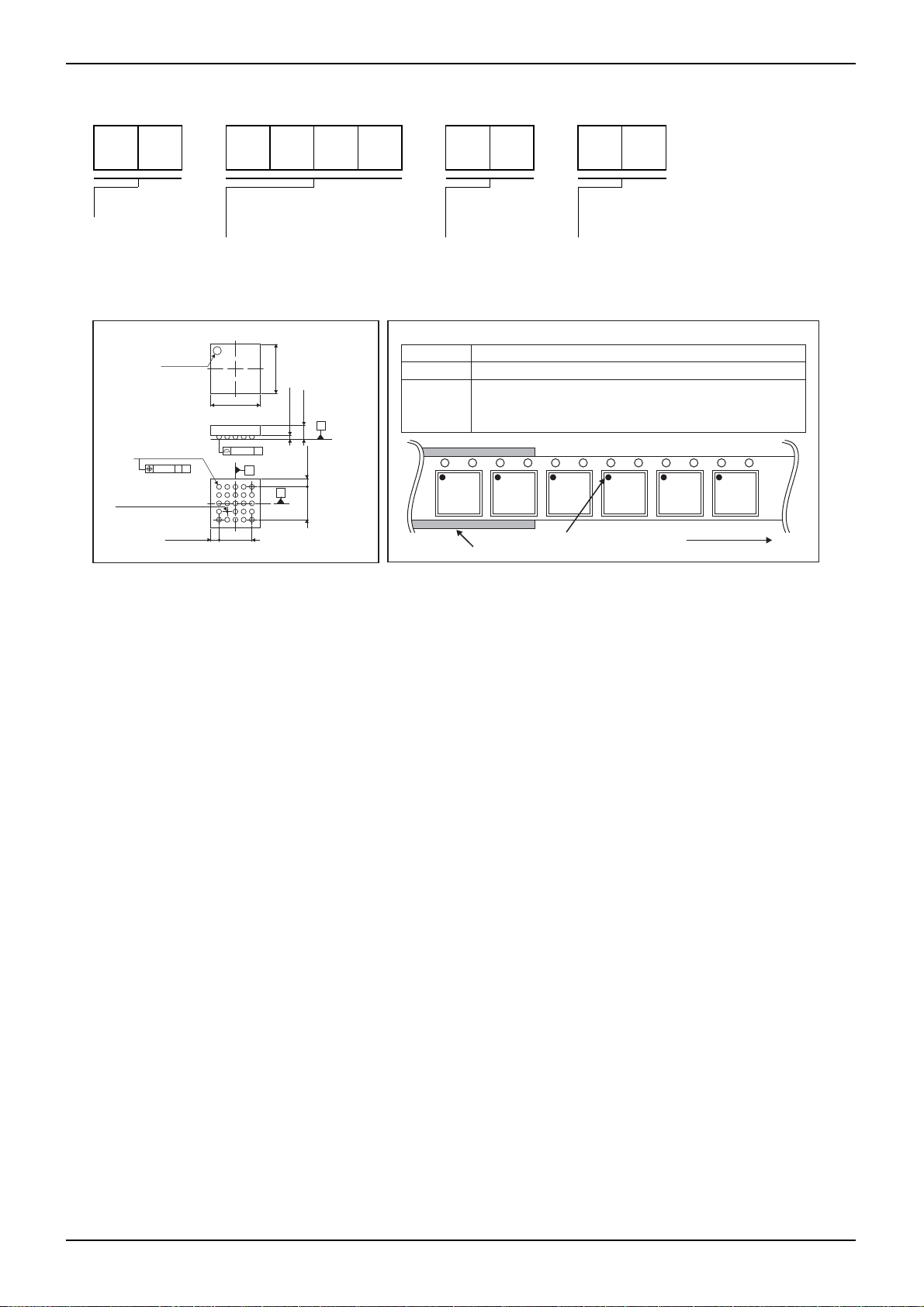
●Ordering part number
B D 2 8 0 2 G U - E 2
Part No. Part No.
2802
VCSP85H2
(φ0.15)INDEX POST
(BD2802GU)
1PIN MARK
24-φ0.30±0.05
0.05
0.4±0.1
BA
2.8±0.1
E
D
C
B
A
12345
P=0.5× 4
0.08 S
A
2.8±0.1
1.0MAX
0.25±0.1
S
0.4±0.1
B
P=0.5× 4
(Unit : mm)
Package
GU : VCSP85H2
<Tape and Reel information>
Embossed carrier tapeTape
Quantity
Direction
of feed
3000pcs
E2
The direction is the 1pin of product is at the upper left when you hold
()
reel on the left hand and you pull out the tape on the right hand
Reel
1pin
Packaging and forming specification
E2: Embossed tape and reel
Direction of feed
Order quantity needs to be multiple of the minimum quantity.
∗
Technical Note
www.rohm.com
© 2011 ROHM Co., Ltd. All rights reserved.
27/27
2011.04 - Rev.
Page 28

Notes
No copying or reproduction of this document, in par t or in whole, is permitted without the
consent of ROHM Co.,Ltd.
The content specied herein is subject to change for improvement without notice.
The content specied herein is for the purpose of introducing ROHM's products (hereinafter
"Products"). If you wish to use any such Product, please be sure to refer to the specications,
which can be obtained from ROHM upon request.
Examples of application circuits, circuit constants and any other information contained herein
illustrate the standard usage and operations of the Products. The peripheral conditions must
be taken into account when designing circuits for mass production.
Great care was taken in ensuring the accuracy of the information specied in this document.
However, should you incur any damage arising from any inaccuracy or misprint of such
information, ROHM shall bear no responsibility for such damage.
The technical information specied herein is intended only to show the typical functions of and
examples of application circuits for the Products. ROHM does not grant you, explicitly or
implicitly, any license to use or exercise intellectual property or other rights held by ROHM and
other parties. ROHM shall bear no responsibility whatsoever for any dispute arising from the
use of such technical information.
The Products specied in this document are intended to be used with general-use electronic
equipment or devices (such as audio visual equipment, ofce-automation equipment, communication devices, electronic appliances and amusement devices).
The Products specied in this document are not designed to be radiation tolerant.
While ROHM always makes effor ts to enhance the quality and reliability of its Products, a
Product may fail or malfunction for a variety of reasons.
Please be sure to implement in your equipment using the Products safety measures to guard
against the possibility of physical injury, re or any other damage caused in the event of the
failure of any Product, such as derating, redundancy, re control and fail-safe designs. ROHM
shall bear no responsibility whatsoever for your use of any Product outside of the prescribed
scope or not in accordance with the instruction manual.
The Products are not designed or manufactured to be used with any equipment, device or
system which requires an extremely high level of reliability the failure or malfunction of which
may result in a direct threat to human life or create a risk of human injury (such as a medical
instrument, transportation equipment, aerospace machiner y, nuclear-reactor controller, fuelcontroller or other safety device). ROHM shall bear no responsibility in any way for use of any
of the Products for the above special purposes. If a Product is intended to be used for any
such special purpose, please contact a ROHM sales representative before purchasing.
If you intend to export or ship overseas any Product or technology specied herein that may
be controlled under the Foreign Exchange and the Foreign Trade Law, you will be required to
obtain a license or permit under the Law.
Notice
www.rohm.com
© 2011 ROHM Co., Ltd. All rights reserved.
Thank you for your accessing to ROHM product informations.
More detail product informations and catalogs are available, please contact us.
ROHM Customer Support System
http://www.rohm.com/contact/
R1120
A
 Loading...