


System LED Drivers for Mobile Phones
7x17(Max.) Dot Matrix
LED Display Driver
BD26502GUL
●Description
BD26502GUL is “Matrix LED Driver” that is the most suitable for the cellular phone.
It can control 7x17(119 dot) LED Matrix by internal 7-channel PMOS SWs and 17-channel LED drivers.
It can control the luminance and firefly lighting of the LED matrix by the setting of the internal register.
It supports SPI and I2C interface.
VCSP50L4 (4.1mm
It adopts the very thin CSP package that is the most suitable for the slim phone.
●Features
1) LED Matrix driver (7x17)
・It has 7-channel PMOS SWs and 17-channel current drivers with 1/7 timing driven sequentially.
・Put ON/OFF(for every dot).
・The current drivers can drive 0-20.00mA current with 16 step(for every dot).
・64 steps of the luminance control by PWM (common setting for all dots)
・Continuous (TDMA off ) lighting function for LED14-LED17
・Easy register setting by A/B 2-side map for each dot.
2) Automatic Slope function
・Cycle time, Slope time can be set for each dot.
3) 8-direction automatic scroll function.
4) Interface
・SPI and I
・For I
5) Thermal shutdown
6) Small and thin CSP package
・62pin VCSP50L4(4.1mm
*This chip is not designed to protect itself against radioactive rays.
*This material may be changed on its way to designing.
*This material is not the official specification.
●Absolute Maximum Ratings (Ta=25
Maximum voltage (note2) VMAX 7 V
Maximum voltage (note1) VIOMAX 4.5 V
Power Dissipation (note3) Pd 1550 mW
Operating Temperature Range Topr -40 ~ +85 ℃
Storage Temperature Range Tstg -55 ~ +150 ℃
note1) VIO,RESETB,CE,SDA,SCL,IFMODE,SYNC,CLKIN,CLKOUT,TEST1,TEST2,TEST3,TESTO, DO terminal
note2) Except the above
note3) Power dissipation deleting is 12.4mW/
The power dissipation of the IC has to be less than the one of the package.
●Operating Conditions (VBAT≥VIO, VINSW≥VBAT, Ta=-40~85 oC)
VBAT input voltage VBAT 2.7 ~ 5.5 V
VINSW input voltage VINSW 2.7 ~ 5.5 V
VIO pin voltage VIO 1.65 ~ 3.3 V
□
0.55mm height max), small and thin type chip size package.
2
C BUS FS mode(max 400kHz)Compatibility
2
C mode, I2C Device address is selectable (74h or 75h)
2
0.55mm height max)
o
C)
Parameter Symbol Ratings Unit
o
C , when it’s used in over 25 oC. (ROHM’s standard board has been mounted.)
Parameter Symbol Limits Unit
No.10041EAT01
www.rohm.com
© 2010 ROHM Co., Ltd. All rights reserved.
1/39
2010.02 - Rev.A

BD26502GUL
●Electrical Characteristics (Unless otherwise specified, Ta=25°C, VBAT=3.6V, VINSW=3.6V, VIO=1.8V)
Parameter Symbol
[ Circuit Current ]
VBAT Circuit current 1 IBAT1 - 0 3.0 A RESETB=0V, VIO=0V
VBAT Circuit current 2 IBAT2 - 0.8 5.0 A RESETB=0V, VIO=1.8V
VBAT Circuit current 3 IBAT3 - 2.0 3.5 mA
[ UVLO ]
UVLO Threshold VUVLO - 2.1 2.5 V VBAT falling
UVLO Hysteresis VHYUVLO 50 - - mV
[ LED Driver ] (LED1-17)
Maximum output current ILEDMax - 20.00 - mA LED1-17 ,ISET=100kΩ
Output current ILED -7.0% 10.67 +7.0% mA I=10.67mA setting, VLED=1V
LED current Matching ILEDMT - - 5 %
Driver pin voltage range VLED 0.2 - VBAT- 1.4 V
Min. Typ. Max.
Limit
Unit Condition
When LED1-17 are active
with default settings.
ILEDMT=
(ILEDMax-ILEDMin)/(ILEDMax+ILEDMin)
I=10.67mA setting, VLED=1V
Technical Note
LED OFF Leak current ILKLED - - 1.0 A
[ PMOS switch ]
Leak current at OFF ILEAKP - - 1.0 A
Resistor at ON RonP - 1.0 - Isw=170mA, VINSW=4.5V
[ OSC ]
OSC frequency fosc 0.96 1.2 1.44 MHz
[ CE, SYNC, CLKIN, IFMODE ]
L level input voltage VIL1 -0.3 - 0.25 x VIO V
H level input voltage VIH1 0.75 x VIO - VIO +0.3 V
L level input current IIL1 - 0 1 A
H level input current IIH1 - 0 1 A
[ SDA, SCL ]
L level input voltage VIL2 -0.3 - 0.25 x VIO V
H level input voltage VIH2 0.75 x VIO - VIO +0.3 V
Input hysteresis Vhys 0.05 x VIO - - V
L level output voltage
(for SDA pin)
Input current Iin1 -3 - 3 A Input voltage = from (0.1 x VIO) to (0.9 x VIO)
VOL2 0 - 0.3 V At 3mA sink current
[ RESETB ]
L level input voltage VIL3 -0.3 - 0.25 x VIO V
H level input voltage VIH3 0.75 x VIO - VIO +0.3 V
Input current Iin2 - 0 1 A Input voltage = from (0.1 x VIO) to (0.9 x VIO)
[ CLKOUT ]
L level output voltage VOL1 - - 0.4 V IOL=2mA
H level output voltage VOH1 0.75 x VIO - - V IOH=-2mA
www.rohm.com
© 2010 ROHM Co., Ltd. All rights reserved.
2/39
2010.02 - Rev.A

BD26502GUL
●Power Dissipation (on the ROHM’s Standard Board)
1.8
1550mW
1.6
1.4
W)
1.2
(
1.0
0.8
0.6
Power Dissipation Pd
0.4
0.2
Technical Note
0.0
0 25 50 75 100 125 150
Ta(℃)
Fig.1
Information of the ROHM’s standard board
Material: glass-epoxy
Size : 50mm×58mm×1.75mm(
8th layer)
Wiring pattern figure Refer to after page.
,
www.rohm.com
© 2010 ROHM Co., Ltd. All rights reserved.
3/39
2010.02 - Rev.A
BD26502GUL
A
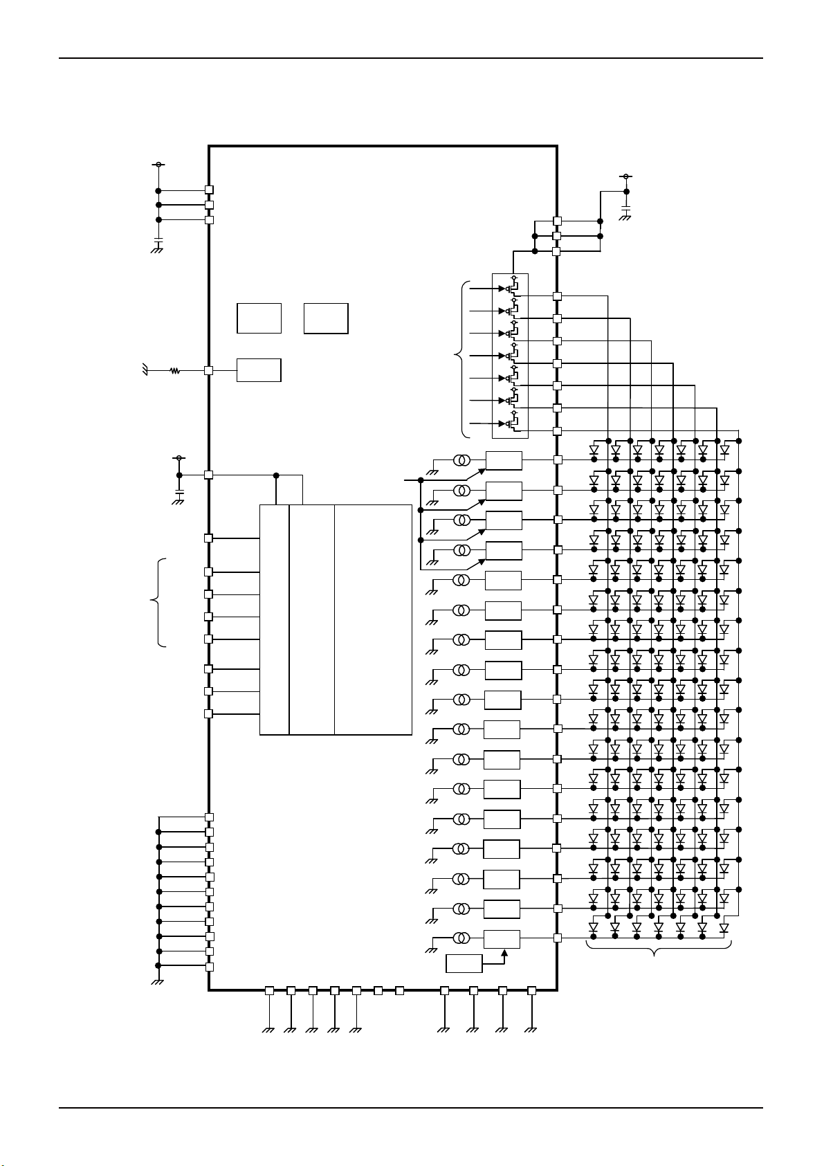
●Block Diagram / Application Circuit Example 1
VBAT
VBAT1
VBAT2
VBAT3
10µF
VREF
OSC
100kΩ
ISET
IREF
VIO
1µF
I2C or SPI
selectable
RESETB
CE
SD
SCL
IFMODE
SYNC
CLKIN
CLKOUT
I/O
Level
Shift
GND1
GND2
GND3
GND4
GND5
GND6
GND7
GND8
GND9
GND10
GND11
TEST1
TEST2
TEST3
TEST4
Fig.2 Block Diagram / Application Circuit example 1
Enable
SPI / I2C
interface
Digital Control
TEST5
TESTO
1.33mA step
DO
Logic
TDMA
20.00mA/ch
LEDGND1
PWM
LEDGND2
T06
T05
T04
T03
T02
T01
T00
TDMA
TDMA
TDMA
TDMA
TDMA
TDMA
TDMA
TDMA
TDMA
TDMA
TDMA
TDMA
TDMA
TDMA
TDMA
TDMA
TDMA
LEDGND3
Technical Note
VINSW
VINSW1
VINSW2
VINSW3
SW7
SW6
SW5
SW4
SW3
SW2
SW1
LED17
LED16
LED15
LED14
LED13
LED12
LED11
LED10
LED9
LED8
LED7
LED6
LED5
LED4
LED3
LED2
LED1
LEDGND4
10F
7×17
Dot Matrix Unit
www.rohm.com
© 2010 ROHM Co., Ltd. All rights reserved.
4/39
2010.02 - Rev.A

BD26502GUL
A
●Block Diagram / Application Circuit Example 2
VBAT
VBAT1
VBAT2
VBAT3
10µF
VREF
OSC
100kΩ
ISET
IREF
VIO
1µF
I2C or SPI
selectable
RESETB
CE
SD
SCL
IFMODE
SYNC
CLKIN
CLKOUT
I/O
Level
Shift
GND1
GND2
GND3
GND4
GND5
GND6
GND7
GND8
GND9
GND10
GND11
TEST1
TEST2
TEST3
TEST4
Fig.3 Block Diagram / Application Circuit example 2
Enable
SPI / I2C
interface
Digital Control
TEST5
TESTO
1.33mA step
DO
Logic
TDMA
20.00mA/ch
LEDGND1
PWM
LEDGND2
T06
T05
T04
T03
T02
T01
T00
TDMA
TDMA
TDMA
TDMA
TDMA
TDMA
TDMA
TDMA
TDMA
TDMA
TDMA
TDMA
TDMA
TDMA
TDMA
TDMA
TDMA
LEDGND3
Technical Note
VINSW
VINSW1
VINSW2
VINSW3
SW7
SW6
SW5
SW4
SW3
SW2
SW1
LED17
LED16
LED15
LED14
LED13
LED12
LED11
LED10
LED9
LED8
LED7
LED6
LED5
LED4
LED3
LED2
LED1
LEDGND4
10F
7×13
Dot Matrix Unit
www.rohm.com
© 2010 ROHM Co., Ltd. All rights reserved.
5/39
2010.02 - Rev.A

BD26502GUL
●Pin Arrangement [Bottom View]
TEST4 LED11 LED12 GND1 LED15 LED16 LED17 TESTO
H
LED9 LED10 LED13 LED14 GND2 CLKOUT CE SDA
G
LED8 ISET LEDGND3 LEDGND4 TEST1 IFMODE SCL VIO
F
LEDGND2 LED7 VBAT1 VBAT2 RESETB CLKIN SYNC DO
E
LED5 LED6 LED4 SW3 SW2 SW1 VINSW1
D
Technical Note
LED3 LEDGND1
C
LED2 LED1 GND4 GND5 GND6 SW6 SW7 VINSW3
B
TEST3 VBAT3 GND7 GND8 GND9 GND10 GND11 TEST5
A
1 2 3 4 5 6 7 8
Total 62 Balls
GND3 TEST2 SW5 SW4 VINSW2
index
www.rohm.com
© 2010 ROHM Co., Ltd. All rights reserved.
6/39
2010.02 - Rev.A

BD26502GUL
●Package
62pin VCSP50L4 CSP small package
SIZE : 4.10mm
Height : 0.55mm max
A ball pitch : 0.5 mm
□
Technical Note
*INDEX POST has No Solder Ball
www.rohm.com
© 2010 ROHM Co., Ltd. All rights reserved.
7/39
2010.02 - Rev.A

BD26502GUL
●Pin Functions
Ball
No
1 A1 TEST3 I 94k GND VIO GND Test input pin 3 E
2 A2 VBAT3 - - VBAT - GND Battery is connected A
3 A3 GND7 - - GND VBAT - Ground B
4 A4 GND8 - - GND VBAT - Ground B
5 A5 GND9 - - GND VBAT - Ground B
6 A6 GND10 - - GND VBAT - Ground B
7 A7 GND11 - - GND VBAT - Ground B
8 A8 TEST5 I - GND VINSW GND Test input pin 5 I
9 B1 LED2 O - GND - GND LED2 driver output K
10 B2 LED1 O - GND - GND LED1 driver output K
11 B3 GND4 - - GND VBAT - Ground B
12 B4 GND5 - - GND VBAT - Ground B
13 B5 GND6 - - GND VBAT - Ground B
14 B6 SW6 O - VINSW VINSW GND P-MOS SW6 output C
15 B7 SW7 O - VINSW VINSW GND P-MOS SW7 output C
16 B8 VINSW3 - - VINSW - GND Power supply for SW1-7 A
17 C1 LED3 O - GND - GND LED3 driver output K
18 C2 LEDGND1 - - GND VBAT - Ground B
19 C4 GND3 - - GND VBAT - Ground B
20 C5 TEST2 I 94k GND VIO GND Test input pin 2 E
21 C6 SW5 O - VINSW VINSW GND P-MOS SW5 output C
22 C7 SW4 O - VINSW VINSW GND P-MOS SW4 output C
23 C8 VINSW2 - - VINSW - GND Power supply for SW1-7 A
24 D1 LED5 O - GND - GND LED5 driver output K
25 D2 LED6 O - GND - GND LED6 driver output K
26 D3 LED4 O - GND - GND LED4 driver output K
27 D5 SW3 O - VINSW VINSW GND P-MOS SW3 output C
28 D6 SW2 O - VINSW VINSW GND P-MOS SW2 output C
29 D7 SW1 O - VINSW VINSW GND P-MOS SW1output C
30 D8 VINSW1 - - VINSW - GND Power supply for SW1-7 A
31 E1 LEDGND2 - - GND VBAT - Ground B
32 E2 LED7 O - GND - GND LED7 driver output K
33 E3 VBAT1 - - VBAT - GND Battery is connected A
34 E4 VBAT2 - - VBAT - GND Battery is connected A
35 E5 RESETB I - GND VIO GND Reset input pin (L: reset, H: reset cancel) D
36 E6 CLKIN I - GND VIO GND External CLK input pin D
37 E7 SYNC I - GND VIO GND External synchronous input pin D
38 E8 DO O - OPEN VIO GND Test output pin2 G
39 F1 LED8 O - GND - GND LED8 driver output K
40 F2 I SET I - OPEN VBAT GND LED Constant Current Driver Current setting pin J
41 F3 LEDGND3 - - GND VBAT - Ground B
42 F4 LEDGND4 - - GND VBAT - Ground B
43 F5 TEST1 I 94k GND VIO GND Test input pin 1 E
44 F6 IFMODE I - GND VIO GND I2C/SPI select pin (L: I2C, H: SPI) D
45 F7 SCL I - GND VIO GND SPI, I2C CLK input pin D
Pin Name I/O
No.
down
Pull
Unused
Terminal
setting
ESD Diode
For
Power
For
Ground
Functions
Technical Note
Equivalent
Circuit
www.rohm.com
© 2010 ROHM Co., Ltd. All rights reserved.
8/39
2010.02 - Rev.A

BD26502GUL
Ball
No
46 F8
47 G1
48 G2
49 G3
50 G4
51 G5
52 G6
53 G7 CE I - GND VIO GND
54 G8
55 H1
56 H2
57 H3
58 H4
59 H5
60 H6
61 H7
62 H8
* Please connect the unused LED pins to the ground.
* It is prohibition to set the registers for unused LED.
Total 62 pins
●Equivalent Circuit
A
Pin Name I/O
No.
VIO - - VIO - GND
LED9 O - GND - GND
LED10 O - GND - GND
LED13 O - GND - GND
LED14 O - GND - GND
GND2 - - GND VBAT -
CLKOUT O - OPEN VIO GND
SDA I/O - GND VIO GND
TEST4 I - GND VBAT GND
LED11 O - GND - GND
LED12 O - GND - GND
GND1 - - GND VBAT -
LED15 O - GND - GND
LED16 O - GND - GND
LED17 O - GND - GND
TESTO O - OPEN VIO GND
down
B
Pull
Unused
Terminal
setting
VBAT
ESD Diode
For
Power
For
Ground
Technical Note
Functions
I/O Power supply is connected
LED9 driver output
LED10 driver output
LED13 driver output
LED14 driver output
Ground
Reference CLK output pin
SPI enable pin(H:Enable), or
2
I
C slave address selection (L: 74h, H: 75h) D
SPI DATA input / I2C DATA input-output pin
Test input pin 4
LED11 driver output
LED12 driver output
Ground
LED15 driver output
LED16 driver output
LED17 driver output
Test output pin1
VINSWCVINSW
D
VIO VIO
Equivalent
Circuit
A
K
K
K
K
B
G
F
H
K
K
B
K
K
K
G
E
I
www.rohm.com
© 2010 ROHM Co., Ltd. All rights reserved.
VIO VIO
VINSW
F
J
VBAT
VIOVIO
VIOG
VIO
H
VBAT
K
9/39
2010.02 - Rev.A

BD26502GUL
●Serial Interface
1. SPI format
・When IFMODE is set to “H”, it can interface with SPI format.
・The serial interface is four terminals (serial clock terminal (SCL), serial data input terminal (SDA), and chip
selection input terminal (CE)).
(1)Write operation
・Data is taken into an internal shift register with rising edge of CLK. (Max of the frequency is 13MHz.)
・The receive data becomes enable in the “H” section of CE. (Active “H”.)
・The transmit data is forwarded (with MSB-First) in the order of write command “0”(1bit), the control register address
(7bit) and data (8bit).
CE
SCL
Technical Note
SDA
W A6 A5 A4 A3 A2 A1 A0 D4 D3 D2 D1 D0 D7 D6 D5
Fig.4 Writing format
(2)Timing diagram
CE
SCL
SDA
tcss tscyc
twhc
tss tsh
twlc
tcgh
tcsw
Fig.5 Timing diagram (SPI format)
(3) Electrical Characteristics (Unless otherwise specified, Ta=25°C, VBAT=3.6V, VINSW=3.6V, VIO=1.8V)
Parameter Symbol
Min Typ Max
Limit
Unit Condition
SCL cycle time tscyc 76 - - ns
H period of SCL cycle Twhc 35 - - ns
L period of SCL cycle twlc 35 - - ns
SDA setup time tss 38 - - ns
SDA hold time tsh 38 - - ns
Read and Write interval tcsw 38 - - ns
CE setup time tcss 55 - - ns
CE hold time tcgh 55 - - ns
www.rohm.com
© 2010 ROHM Co., Ltd. All rights reserved.
10/39
2010.02 - Rev.A

BD26502GUL
2. I2C BUS format
When IFMODE is set to “L”, it can interface with I2C BUS format.
(1) Slave address
CE A7 A6 A5 A4 A3 A2 A1 R/W
L 1 1 1 0 1 0 0
H 1 1 1 0 1 0 1
(2) Bit Transfer
SCL transfers 1-bit data during H. During H of SCL, SDA cannot be changed at the time of bit transfer. If SDA changes
while SCL is H, START conditions or STOP conditions will occur and it will be interpreted as a control signal.
(3) START and STOP condition
When SDA and SCL are H, data is not transferred on the I
while SCL has been H, it will become START (S) conditions, and an access start, if SDA changes from L to H while SCL
has been H, it will become STOP (P) conditions and an access end.
SDA
SCL
SDA
SDA a state of stability
Data are effective
Fig.6 Bit transfer (I
Technical Note
0
SDA
:
It can change
2
C format)
2
C- bus. This condition indicates, if SDA changes from H to L
(4) Acknowledge
SCL
S P
START condition
Fig.7 START/STOP condition (I
2
STOP condition
C format)
It transfers data 8 bits each after the occurrence of START condition. A transmitter opens SDA after transfer 8bits data,
and a receiver returns the acknowledge signal by setting SDA to L.
DATA OUTPUT
BY TRANSMITTER
DATA OUTPUT
BY RECEIVER
SCL
START condition
S
12 89
Fig.8 Acknowledge (I
2
C format)
not acknowledge
acknowledge
clock pulse for
acknowledgement
www.rohm.com
© 2010 ROHM Co., Ltd. All rights reserved.
11/3 9
2010.02 - Rev.A

BD26502GUL
A A
A
A
A7 A6 A5A4A3A2A1A
A
A
S
(5) Writing protocol
A register address is transferred by the next 1 byte that transferred the slave address and the write-in command. The
3rd byte writes data in the internal register written in by the 2nd byte, and after 4th byte or, the increment of register
address is carried out automatically. However, when a register address turns into the last address (77h), it is set to 00h
by the next transmission. After the transmission end, the increment of the address is carried out.
Technical Note
*1 *1
X X X X X X X
S
R/W=0(write)
from master to slave
from slave to master
register addressslave address
(6) Timing diagram
SDA
SU;DAT
t
t HIGH
CL
LOW
t
HD;STA
t
HD;DAT
S Sr P
t
Fig.9 Timing diagram (I2C format)
(7) Electrical Characteristics(Unless otherwise specified, Ta=25
Parameter Symbol
2
【I
C BUS format】
D7D6D5D4D3D2 D1 D0 D7 D6 D5 D4 D3 D2 D1 D0
00
DATA
register address
increment
=acknowledge(SDA LOW)
=not acknowledge(SDA HIGH)
S=START condition
P=STOP condition
*1: Write Timing
t
HD;STA
SU;STA
t
o
C, VBAT=3.6V, VINSW=3.6V, VIO=1.8V)
t SU;STO
DATA
BUF
t
S
Standard-mode Fast-mode
Min. Typ. Max. Min. Typ. Max.
P
register address
increment
Unit
SCL clock frequency fSCL 0 - 100 0 - 400 kHz
LOW period of the SCL clock tLOW 4.7 - - 1.3 - - s
HIGH period of the SCL clock tHIGH 4.0 - - 0.6 - - s
Hold time (repeated) START condition
After this period, the first clock is generated
HD;STA 4.0 - - 0.6 - - s
t
Set-up time for a repeated START condition tSU;STA 4.7 - - 0.6 - - s
Data hold time tHD;DAT 0 - 3.45 0 - 0.9 s
Data set-up time tSU;DAT 250 - - 100 - - ns
Set-up time for STOP condition tSU;STO 4.0 - - 0.6 - - s
Bus free time between a STOP
and START condition
t
BUF 4.7 - - 1.3 - - s
www.rohm.com
© 2010 ROHM Co., Ltd. All rights reserved.
12/39
2010.02 - Rev.A

BD26502GUL
A
Technical Note
●Register List
* Please be sure to write “0” in the register which is not assigned.
* It is prohibition to write data to the address which is not assigned.
Control register
ddress Default D7 D6 D5 D4 D3 D2 D1 D0 Block R/W Remark
00h 00h - - - - - - - SFTRST RESET W
01h 00h - - - - OSCEN - - - OSC W
11h 00h - - LED6ON LED5ON LED4ON LED3ON LED2ON LED1ON
12h 00h - - LED12ON LED11ON LED10ON LED9ON LED8ON LED7ON W
13h 00h - - - LED17ON LED16ON LED15ON LED14ON LED13ON W
17h 0Fh - - - -
20h 00h - - PWMSET[5:0] PWM W
21h 00h - - - - SYNCACT SYNCON CLKOUT CLKIN CLK W
2Dh 00h - - - - - PWMEN SLPEN SCLEN
2Eh 00h - - - - - - - SCLRST W
2Fh 00h - SCLSPEED[2:0] UP DOWN RIGHT LEFT W
30h 00h - - - - - - - START W
31h 00h - - - - - - CLRB CLRA W
7Fh 00h - - - - - IAB OAB RMCG RMAP W
LED17
TDMAON
LED16
TDMAON
LED15
TDMAON
LED14
TDMAON
LED
driver
MATRIX
Software Reset
OSC ON/OFF control
W
LED1-6 Enable
LED7-12 Enable
LED13-17 Enable
W
LED14-17 TDMA Enable
LED1-17PWM DutySetting
CLK selection, SYNC operation control
W
PWM,SLOPE,SCROLL ON/OFF setting
Reset SCROLL
SCROLL Setting
LED matrix control
Matrix data clear
Resister map change
www.rohm.com
© 2010 ROHM Co., Ltd. All rights reserved.
13/39
2010.02 - Rev.A

BD26502GUL
A-pattern register
Address default D7 D6 D5 D4 D3 D2 D1 D0 Block R/W Remark
01h 08h SCYCA00[1:0] SDLYA00[1:0] ILEDA00SET[3:0]
02h 08h SCYCA01[1:0] SDLYA01[1:0] ILEDA01SET[3:0] W
03h 08h SCYCA02[1:0] SDLYA02[1:0] ILEDA02SET[3:0] W
04h 08h SCYCA03[1:0] SDLYA03[1:0] ILEDA03SET[3:0] W
05h 08h SCYCA04[1:0] SDLYA04[1:0] ILEDA04SET[3:0] W
06h 08h SCYCA05[1:0] SDLYA05[1:0] ILEDA05SET[3:0] W
07h 08h SCYCA06[1:0] SDLYA06[1:0] ILEDA06SET[3:0] W
08h 08h SCYCA10[1:0] SDLYA10[1:0] ILEDA10SET[3:0] W
09h 08h SCYCA11[1:0] SDLYA11[1:0] ILEDA11SET[3:0] W
0Ah 08h SCYCA12[1:0] SDLYA12[1:0] ILEDA12SET[3:0] W
0Bh 08h SCYCA13[1:0] SDLYA13[1:0] ILEDA13SET[3:0] W
0Ch 08h SCYCA14[1:0] SDLYA14[1:0] ILEDA14SET[3:0] W
0Dh 08h SCYCA15[1:0] SDLYA15[1:0] ILEDA15SET[3:0] W
0Eh 08h SCYCA16[1:0] SDLYA16[1:0] ILEDA16SET[3:0] W
0Fh 08h SCYCA20[1:0] SDLYA20[1:0] ILEDA20SET[3:0] W
10h 08h SCYCA21[1:0] SDLYA21[1:0] ILEDA21SET[3:0] W
11h 08h SCYCA22[1:0] SDLYA22[1:0] ILEDA22SET[3:0] W
12h 08h SCYCA23[1:0] SDLYA23[1:0] ILEDA23SET[3:0] W
13h 08h SCYCA24[1:0] SDLYA24[1:0] ILEDA24SET[3:0] W
14h 08h SCYCA25[1:0] SDLYA25[1:0] ILEDA25SET[3:0] W
15h 08h SCYCA26[1:0] SDLYA26[1:0] ILEDA26SET[3:0] W
16h 08h SCYCA30[1:0] SDLYA30[1:0] ILEDA30SET[3:0] W
17h 08h SCYCA31[1:0] SDLYA31[1:0] ILEDA31SET[3:0] W
18h 08h SCYCA32[1:0] SDLYA32[1:0] ILEDA32SET[3:0] W
19h 08h SCYCA33[1:0] SDLYA33[1:0] ILEDA33SET[3:0] W
1Ah 08h SCYCA34[1:0] SDLYA34[1:0] ILEDA34SET[3:0] W
1Bh 08h SCYCA35[1:0] SDLYA35[1:0] ILEDA35SET[3:0] W
1Ch 08h SCYCA36[1:0] SDLYA36[1:0] ILEDA36SET[3:0] W
1Dh 08h SCYCA40[1:0] SDLYA40[1:0] ILEDA40SET[3:0] W
1Eh 08h SCYCA41[1:0] SDLYA41[1:0] ILEDA41SET[3:0] W
1Fh 08h SCYCA42[1:0] SDLYA42[1:0] ILEDA42SET[3:0] W
20h 08h SCYCA43[1:0] SDLYA43[1:0] ILEDA43SET[3:0] W
21h 08h SCYCA44[1:0] SDLYA44[1:0] ILEDA44SET[3:0] W
22h 08h SCYCA45[1:0] SDLYA45[1:0] ILEDA45SET[3:0] W
23h 08h SCYCA46[1:0] SDLYA46[1:0] ILEDA46SET[3:0] W
24h 08h SCYCA50[1:0] SDLYA50[1:0] ILEDA50SET[3:0] W
25h 08h SCYCA51[1:0] SDLYA51[1:0] ILEDA51SET[3:0] W
26h 08h SCYCA52[1:0] SDLYA52[1:0] ILEDA52SET[3:0] W
27h 08h SCYCA53[1:0] SDLYA53[1:0] ILEDA53SET[3:0] W
28h 08h SCYCA54[1:0] SDLYA54[1:0] ILEDA54SET[3:0] W
29h 08h SCYCA55[1:0] SDLYA55[1:0] ILEDA55SET[3:0] W
2Ah 08h SCYCA56[1:0] SDLYA56[1:0] ILEDA56SET[3:0] W
2Bh 08h SCYCA60[1:0] SDLYA60[1:0] ILEDA60SET[3:0] W
2Ch 08h SCYCA61[1:0] SDLYA61[1:0] ILEDA61SET[3:0] W
2Dh 08h SCYCA62[1:0] SDLYA62[1:0] ILEDA62SET[3:0] W
2Eh 08h SCYCA63[1:0] SDLYA63[1:0] ILEDA63SET[3:0] W
2Fh 08h SCYCA64[1:0] SDLYA64[1:0] ILEDA64SET[3:0] W
30h 08h SCYCA65[1:0] SDLYA65[1:0] ILEDA65SET[3:0] W
MATRIX
Data
W
Data for Matrix 00(DA00)
Data for Matrix 01(DA01)
Data for Matrix 02(DA02)
Data for Matrix 03(DA03)
Data for Matrix 04(DA04)
Data for Matrix 05(DA05)
Data for Matrix 06(DA06)
Data for Matrix 10(DA10)
Data for Matrix 11(DA11)
Data for Matrix 12(DA12)
Data for Matrix 13(DA13)
Data for Matrix 14(DA14)
Data for Matrix 15(DA15)
Data for Matrix 16(DA16)
Data for Matrix 20(DA20)
Data for Matrix 21(DA21)
Data for Matrix 22(DA22)
Data for Matrix 23(DA23)
Data for Matrix 24(DA24)
Data for Matrix 25(DA25)
Data for Matrix 26(DA26)
Data for Matrix 30(DA30)
Data for Matrix 31(DA31)
Data for Matrix 32(DA32)
Data for Matrix 33(DA33)
Data for Matrix 34(DA34)
Data for Matrix 35(DA35)
Data for Matrix 36(DA36)
Data for Matrix 40(DA40)
Data for Matrix 41(DA41)
Data for Matrix 42(DA42)
Data for Matrix 43(DA43)
Data for Matrix 44(DA44)
Data for Matrix 45(DA45)
Data for Matrix 46(DA46)
Data for Matrix 50(DA50)
Data for Matrix 51(DA51)
Data for Matrix 52(DA52)
Data for Matrix 53(DA53)
Data for Matrix 54(DA54)
Data for Matrix 55(DA55)
Data for Matrix 56(DA56)
Data for Matrix 60(DA60)
Data for Matrix 61(DA61)
Data for Matrix 62(DA62)
Data for Matrix 63(DA63)
Data for Matrix 64(DA64)
Data for Matrix 65(DA65)
Technical Note
www.rohm.com
© 2010 ROHM Co., Ltd. All rights reserved.
14/39
2010.02 - Rev.A

BD26502GUL
Address default D7 D6 D5 D4 D3 D2 D1 D0 Block R/W Remark
31h 08h SCYCA66[1:0] SDLYA66[1:0] ILEDA66SET[3:0]
32h 08h SCYCA70[1:0] SDLYA70[1:0] ILEDA70SET[3:0] W Data for Matrix 70(DA70)
33h 08h SCYCA71[1:0] SDLYA71[1:0] ILEDA71SET[3:0] W Data for Matrix 71(DA71)
34h 08h SCYCA72[1:0] SDLYA72[1:0] ILEDA72SET[3:0] W Data for Matrix 72(DA72)
35h 08h SCYCA73[1:0] SDLYA73[1:0] ILEDA73SET[3:0] W Data for Matrix 73(DA73)
36h 08h SCYCA74[1:0] SDLYA74[1:0] ILEDA74SET[3:0] W Data for Matrix 74(DA74)
37h 08h SCYCA75[1:0] SDLYA75[1:0] ILEDA75SET[3:0] W Data for Matrix 75(DA75)
38h 08h SCYCA76[1:0] SDLYA76[1:0] ILEDA76SET[3:0] W Data for Matrix 76(DA76)
39h 08h SCYCA80[1:0] SDLYA80[1:0] ILEDA80SET[3:0] W Data for Matrix 80(DA80)
3Ah 08h SCYCA81[1:0] SDLYA81[1:0] ILEDA81SET[3:0] W Data for Matrix 81(DA81)
3Bh 08h SCYCA82[1:0] SDLYA82[1:0] ILEDA82SET[3:0] W Data for Matrix 82(DA82)
3Ch 08h SCYCA83[1:0] SDLYA83[1:0] ILEDA83SET[3:0] W Data for Matrix 83(DA83)
3Dh 08h SCYCA84[1:0] SDLYA84[1:0] ILEDA84SET[3:0] W Data for Matrix 84(DA84)
3Eh 08h SCYCA85[1:0] SDLYA85[1:0] ILEDA85SET[3:0] W Data for Matrix 85(DA85)
3Fh 08h SCYCA86[1:0] SDLYA86[1:0] ILEDA86SET[3:0] W Data for Matrix 86(DA86)
40h 08h SCYCA90[1:0] SDLYA90[1:0] ILEDA90SET[3:0] W Data for Matrix 90(DA90)
41h 08h SCYCA91[1:0] SDLYA91[1:0] ILEDA91SET[3:0] W Data for Matrix 91(DA91)
42h 08h SCYCA92[1:0] SDLYA92[1:0] ILEDA92SET[3:0] W Data for Matrix 92(DA92)
43h 08h SCYCA93[1:0] SDLYA93[1:0] ILEDA93SET[3:0] W Data for Matrix 93(DA93)
44h 08h SCYCA94[1:0] SDLYA94[1:0] ILEDA94SET[3:0] W Data for Matrix 94(DA94)
45h 08h SCYCA95[1:0] SDLYA95[1:0] ILEDA95SET[3:0] W Data for Matrix 95(DA95)
46h 08h SCYCA96[1:0] SDLYA96[1:0] ILEDA96SET[3:0] W Data for Matrix 96(DA96)
47h 08h SCYCAA0[1:0] SDLYAA0[1:0] ILEDAA0SET[3:0] W Data for Matrix A0(DAA0)
48h 08h SCYCAA1[1:0] SDLYAA1[1:0] ILEDAA1SET[3:0] W Data for Matrix A1(DAA1)
49h 08h SCYCAA2[1:0] SDLYAA2[1:0] ILEDAA2SET[3:0] W Data for Matrix A2(DAA2)
4Ah 08h SCYCAA3[1:0] SDLYAA3[1:0] ILEDAA3SET[3:0] W Data for Matrix A3(DAA3)
4Bh 08h SCYCAA4[1:0] SDLYAA4[1:0] ILEDAA4SET[3:0] W Data for Matrix A4(DAA4)
4Ch 08h SCYCAA5[1:0] SDLYAA5[1:0] ILEDAA5SET[3:0] W Data for Matrix A5(DAA5)
4Dh 08h SCYCAA6[1:0] SDLYAA6[1:0] ILEDAA6SET[3:0] W Data for Matrix A6(DAA6)
4Eh 08h SCYCAB0[1:0] SDLYAB0[1:0] ILEDAB0SET[3:0] W Data for Matrix B0(DAB0)
4Fh 08h SCYCAB1[1:0] SDLYAB1[1:0] ILEDAB1SET[3:0] W Data for Matrix B1(DAB1)
50h 08h SCYCAB2[1:0] SDLYAB2[1:0] ILEDAB2SET[3:0] W Data for Matrix B2(DAB2)
51h 08h SCYCAB3[1:0] SDLYAB3[1:0] ILEDAB3SET[3:0] W Data for Matrix B3(DAB3)
52h 08h SCYCAB4[1:0] SDLYAB4[1:0] ILEDAB4SET[3:0] W Data for Matrix B4(DAB4)
53h 08h SCYCAB5[1:0] SDLYAB5[1:0] ILEDAB5SET[3:0] W Data for Matrix B5(DAB5)
54h 08h SCYCAB6[1:0] SDLYAB6[1:0] ILEDAB6SET[3:0] W Data for Matrix B6(DAB6)
55h 08h SCYCAC0[1:0] SDLYAC0[1:0] ILEDAC0SET[3:0] W Data for Matrix C0(DAC0)
56h 08h SCYCAC1[1:0] SDLYAC1[1:0] ILEDAC1SET[3:0] W Data for Matrix C1(DAC1)
57h 08h SCYCAC2[1:0] SDLYAC2[1:0] ILEDAC2SET[3:0] W Data for Matrix C2(DAC2)
58h 08h SCYCAC3[1:0] SDLYAC3[1:0] ILEDAC3SET[3:0] W Data for Matrix C3(DAC3)
59h 08h SCYCAC4[1:0] SDLYAC4[1:0] ILEDAC4SET[3:0] W Data for Matrix C4(DAC4)
5Ah 08h SCYCAC5[1:0] SDLYAC5[1:0] ILEDAC5SET[3:0] W Data for Matrix C5(DAC5)
5Bh 08h SCYCAC6[1:0] SDLYAC6[1:0] ILEDAC6SET[3:0] W Data for Matrix C6(DAC6)
5Ch 08h SCYCAD0[1:0] SDLYAD0[1:0] ILEDAD0SET[3:0] W Data for Matrix D0(DAD0)
5Dh 08h SCYCAD1[1:0] SDLYAD1[1:0] ILEDAD1SET[3:0] W Data for Matrix D1(DAD1)
5Eh 08h SCYCAD2[1:0] SDLYAD2[1:0] ILEDAD2SET[3:0] W Data for Matrix D2(DAD2)
5Fh 08h SCYCAD3[1:0] SDLYAD3[1:0] ILEDAD3SET[3:0] W Data for Matrix D3(DAD3)
60h 08h SCYCAD4[1:0] SDLYAD4[1:0] ILEDAD4SET[3:0] W Data for Matrix D4(DAD4)
MATRIX
Data
W Data for Matrix 66(DA66)
Technical Note
www.rohm.com
© 2010 ROHM Co., Ltd. All rights reserved.
15/39
2010.02 - Rev.A

BD26502GUL
Address default D7 D6 D5 D4 D3 D2 D1 D0 Block R/W Remark
61h 08h SCYCAD5[1:0] SDLYAD5[1:0] ILEDAD5SET[3:0]
62h 08h SCYCAD6[1:0] SDLYAD6[1:0] ILEDAD6SET[3:0] W Data for Matrix D6(DAD6)
63h 08h SCYCAE0[1:0] SDLYAE0[1:0] ILEDAE0SET[3:0] W Data for Matrix E0(DAE0)
64h 08h SCYCAE1[1:0] SDLYAE1[1:0] ILEDAE1SET[3:0] W Data for Matrix E1(DAE1)
65h 08h SCYCAE2[1:0] SDLYAE2[1:0] ILEDAE2SET[3:0] W Data for Matrix E2(DAE2)
66h 08h SCYCAE3[1:0] SDLYAE3[1:0] ILEDAE3SET[3:0] W Data for Matrix E3(DAE3)
67h 08h SCYCAE4[1:0] SDLYAE4[1:0] ILEDAE4SET[3:0] W Data for Matrix E4(DAE4)
68h 08h SCYCAE5[1:0] SDLYAE5[1:0] ILEDAE5SET[3:0] W Data for Matrix E5(DAE5)
69h 08h SCYCAE6[1:0] SDLYAE6[1:0] ILEDAE6SET[3:0] W Data for Matrix E6(DAE6)
6Ah 08h SCYCAF0[1:0] SDLYAF0[1:0] ILEDAF0SET[3:0] W Data for Matrix F0(DAF0)
6Bh 08h SCYCAF1[1:0] SDLYAF1[1:0] ILEDAF1SET[3:0] W Data for Matrix F1(DAF1)
6Ch 08h SCYCAF2[1:0] SDLYAF2[1:0] ILEDAF2SET[3:0] W Data for Matrix F2(DAF2)
6Dh 08h SCYCAF3[1:0] SDLYAF3[1:0] ILEDAF3SET[3:0] W Data for Matrix F3(DAF3)
6Eh 08h SCYCAF4[1:0] SDLYAF4[1:0] ILEDAF4SET[3:0] W Data for Matrix F4(DAF4)
6Fh 08h SCYCAF5[1:0] SDLYAF5[1:0] ILEDAF5SET[3:0] W Data for Matrix F5(DAF5)
70h 08h SCYCAF6[1:0] SDLYAF6[1:0] ILEDAF6SET[3:0] W Data for Matrix F6(DAF6)
71h 08h SCYCAG0[1:0] SDLYAG0[1:0] ILEDAG0SET[3:0] W Data for Matrix G0(DAG0)
72h 08h SCYCAG1[1:0] SDLYAG1[1:0] ILEDAG1SET[3:0] W Data for Matrix G1(DAG1)
73h 08h SCYCAG2[1:0] SDLYAG2[1:0] ILEDAG2SET[3:0] W Data for Matrix G2(DAG2)
74h 08h SCYCAG3[1:0] SDLYAG3[1:0] ILEDAG3SET[3:0] W Data for Matrix G3(DAG3)
75h 08h SCYCAG4[1:0] SDLYAG4[1:0] ILEDAG4SET[3:0] W Data for Matrix G4(DAG4)
76h 08h SCYCAG5[1:0] SDLYAG5[1:0] ILEDAG5SET[3:0] W Data for Matrix G5(DAG5)
77h 08h SCYCAG6[1:0] SDLYAG6[1:0] ILEDAG6SET[3:0] W Data for Matrix G6(DAG6)
MATRIX
Data
W Data for Matrix D5(DAD5)
Technical Note
www.rohm.com
© 2010 ROHM Co., Ltd. All rights reserved.
16/39
2010.02 - Rev.A

BD26502GUL
B-pattern register
Address default D7 D6 D5 D4 D3 D2 D1 D0 Block R/W Remark
01h 08h SCYCB00[1:0] SDLYB00[1:0] ILEDB00SET[3:0]
02h 08h SCYCB01[1:0] SDLYB01[1:0] ILEDB01SET[3:0] W Data for Matrix 01(DB01)
03h 08h SCYCB02[1:0] SDLYB02[1:0] ILEDB02SET[3:0] W Data for Matrix 02(DB02)
04h 08h SCYCB03[1:0] SDLYB03[1:0] ILEDB03SET[3:0] W Data for Matrix 03(DB03)
05h 08h SCYCB04[1:0] SDLYB04[1:0] ILEDB04SET[3:0] W Data for Matrix 04(DB04)
06h 08h SCYCB05[1:0] SDLYB05[1:0] ILEDB05SET[3:0] W Data for Matrix 05(DB05)
07h 08h SCYCB06[1:0] SDLYB06[1:0] ILEDB06SET[3:0] W Data for Matrix 06(DB06)
08h 08h SCYCB10[1:0] SDLYB10[1:0] ILEDB10SET[3:0] W Data for Matrix 10(DB10)
09h 08h SCYCB11[1:0] SDLYB11[1:0] ILEDB11SET[3:0] W Data for Matrix 11(DB11)
0Ah 08h SCYCB12[1:0] SDLYB12[1:0] ILEDB12SET[3:0] W Data for Matrix 12(DB12)
0Bh 08h SCYCB13[1:0] SDLYB13[1:0] ILEDB13SET[3:0] W Data for Matrix 13(DB13)
0Ch 08h SCYCB14[1:0] SDLYB14[1:0] ILEDB14SET[3:0] W Data for Matrix 14(DB14)
0Dh 08h SCYCB15[1:0] SDLYB15[1:0] ILEDB15SET[3:0] W Data for Matrix 15(DB15)
0Eh 08h SCYCB16[1:0] SDLYB16[1:0] ILEDB16SET[3:0] W Data for Matrix 16(DB16)
0Fh 08h SCYCB20[1:0] SDLYB20[1:0] ILEDB20SET[3:0] W Data for Matrix 20(DB20)
10h 08h SCYCB21[1:0] SDLYB21[1:0] ILEDB21SET[3:0] W Data for Matrix 21(DB21)
11h 08h SCYCB22[1:0] SDLYB22[1:0] ILEDB22SET[3:0] W Data for Matrix 22(DB22)
12h 08h SCYCB23[1:0] SDLYB23[1:0] ILEDB23SET[3:0] W Data for Matrix 23(DB23)
13h 08h SCYCB24[1:0] SDLYB24[1:0] ILEDB24SET[3:0] W Data for Matrix 24(DB24)
14h 08h SCYCB25[1:0] SDLYB25[1:0] ILEDB25SET[3:0] W Data for Matrix 25(DB25)
15h 08h SCYCB26[1:0] SDLYB26[1:0] ILEDB26SET[3:0] W Data for Matrix 26(DB26)
16h 08h SCYCB30[1:0] SDLYB30[1:0] ILEDB30SET[3:0] W Data for Matrix 30(DB30)
17h 08h SCYCB31[1:0] SDLYB31[1:0] ILEDB31SET[3:0] W Data for Matrix 31(DB31)
18h 08h SCYCB32[1:0] SDLYB32[1:0] ILEDB32SET[3:0] W Data for Matrix 32(DB32)
19h 08h SCYCB33[1:0] SDLYB33[1:0] ILEDB33SET[3:0] W Data for Matrix 33(DB33)
1Ah 08h SCYCB34[1:0] SDLYB34[1:0] ILEDB34SET[3:0] W Data for Matrix 34(DB34)
1Bh 08h SCYCB35[1:0] SDLYB35[1:0] ILEDB35SET[3:0] W Data for Matrix 35(DB35)
1Ch 08h SCYCB36[1:0] SDLYB36[1:0] ILEDB36SET[3:0] W Data for Matrix 36(DB36)
1Dh 08h SCYCB40[1:0] SDLYB40[1:0] ILEDB40SET[3:0] W Data for Matrix 40(DB40)
1Eh 08h SCYCB41[1:0] SDLYB41[1:0] ILEDB41SET[3:0] W Data for Matrix 41(DB41)
1Fh 08h SCYCB42[1:0] SDLYB42[1:0] ILEDB42SET[3:0] W Data for Matrix 42(DB42)
20h 08h SCYCB43[1:0] SDLYB43[1:0] ILEDB43SET[3:0] W Data for Matrix 43(DB43)
21h 08h SCYCB44[1:0] SDLYB44[1:0] ILEDB44SET[3:0] W Data for Matrix 44(DB44)
22h 08h SCYCB45[1:0] SDLYB45[1:0] ILEDB45SET[3:0] W Data for Matrix 45(DB45)
23h 08h SCYCB46[1:0] SDLYB46[1:0] ILEDB46SET[3:0] W Data for Matrix 46(DB46)
24h 08h SCYCB50[1:0] SDLYB50[1:0] ILEDB50SET[3:0] W Data for Matrix 50(DB50)
25h 08h SCYCB51[1:0] SDLYB51[1:0] ILEDB51SET[3:0] W Data for Matrix 51(DB51)
26h 08h SCYCB52[1:0] SDLYB52[1:0] ILEDB52SET[3:0] W Data for Matrix 52(DB52)
27h 08h SCYCB53[1:0] SDLYB53[1:0] ILEDB53SET[3:0] W Data for Matrix 53(DB53)
28h 08h SCYCB54[1:0] SDLYB54[1:0] ILEDB54SET[3:0] W Data for Matrix 54(DB54)
29h 08h SCYCB55[1:0] SDLYB55[1:0] ILEDB55SET[3:0] W Data for Matrix 55(DB55)
2Ah 08h SCYCB56[1:0] SDLYB56[1:0] ILEDB56SET[3:0] W Data for Matrix 56(DB56)
2Bh 08h SCYCB60[1:0] SDLYB60[1:0] ILEDB60SET[3:0] W Data for Matrix 60(DB60)
2Ch 08h SCYCB61[1:0] SDLYB61[1:0] ILEDB61SET[3:0] W Data for Matrix 61(DB61)
2Dh 08h SCYCB62[1:0] SDLYB62[1:0] ILEDB62SET[3:0] W Data for Matrix 62(DB62)
2Eh 08h SCYCB63[1:0] SDLYB63[1:0] ILEDB63SET[3:0] W Data for Matrix 63(DB63)
2Fh 08h SCYCB64[1:0] SDLYB64[1:0] ILEDB64SET[3:0] W Data for Matrix 64(DB64)
30h 08h SCYCB65[1:0] SDLYB65[1:0] ILEDB65SET[3:0] W Data for Matrix 65(DB65)
MATRIX
Data
W Data for Matrix 00(DB00)
Technical Note
www.rohm.com
© 2010 ROHM Co., Ltd. All rights reserved.
17/39
2010.02 - Rev.A

BD26502GUL
Address default D7 D6 D5 D4 D3 D2 D1 D0 Block R/W Remark
31h 08h SCYCB66[1:0] SDLYB66[1:0] ILEDB66SET[3:0]
32h 08h SCYCB70[1:0] SDLYB70[1:0] ILEDB70SET[3:0] W Data for Matrix 70(DB70)
33h 08h SCYCB71[1:0] SDLYB71[1:0] ILEDB71SET[3:0] W Data for Matrix 71(DB71)
34h 08h SCYCB72[1:0] SDLYB72[1:0] ILEDB72SET[3:0] W Data for Matrix 72(DB72)
35h 08h SCYCB73[1:0] SDLYB73[1:0] ILEDB73SET[3:0] W Data for Matrix 73(DB73)
36h 08h SCYCB74[1:0] SDLYB74[1:0] ILEDB74SET[3:0] W Data for Matrix 74(DB74)
37h 08h SCYCB75[1:0] SDLYB75[1:0] ILEDB75SET[3:0] W Data for Matrix 75(DB75)
38h 08h SCYCB76[1:0] SDLYB76[1:0] ILEDB76SET[3:0] W Data for Matrix 76(DB76)
39h 08h SCYCB80[1:0] SDLYB80[1:0] ILEDB80SET[3:0] W Data for Matrix 80(DB80)
3Ah 08h SCYCB81[1:0] SDLYB81[1:0] ILEDB81SET[3:0] W Data for Matrix 81(DB81)
3Bh 08h SCYCB82[1:0] SDLYB82[1:0] ILEDB82SET[3:0] W Data for Matrix 82(DB82)
3Ch 08h SCYCB83[1:0] SDLYB83[1:0] ILEDB83SET[3:0] W Data for Matrix 83(DB83)
3Dh 08h SCYCB84[1:0] SDLYB84[1:0] ILEDB84SET[3:0] W Data for Matrix 84(DB84)
3Eh 08h SCYCB85[1:0] SDLYB85[1:0] ILEDB85SET[3:0] W Data for Matrix 85(DB85)
3Fh 08h SCYCB86[1:0] SDLYB86[1:0] ILEDB86SET[3:0] W Data for Matrix 86(DB86)
40h 08h SCYCB90[1:0] SDLYB90[1:0] ILEDB90SET[3:0] W Data for Matrix 90(DB90)
41h 08h SCYCB91[1:0] SDLYB91[1:0] ILEDB91SET[3:0] W Data for Matrix 91(DB91)
42h 08h SCYCB92[1:0] SDLYB92[1:0] ILEDB92SET[3:0] W Data for Matrix 92(DB92)
43h 08h SCYCB93[1:0] SDLYB93[1:0] ILEDB93SET[3:0] W Data for Matrix 93(DB93)
44h 08h SCYCB94[1:0] SDLYB94[1:0] ILEDB94SET[3:0] W Data for Matrix 94(DB94)
45h 08h SCYCB95[1:0] SDLYB95[1:0] ILEDB95SET[3:0] W Data for Matrix 95(DB95)
46h 08h SCYCB96[1:0] SDLYB96[1:0] ILEDB96SET[3:0] W Data for Matrix 96(DB96)
47h 08h SCYCBA0[1:0] SDLYBA0[1:0] ILEDBA0SET[3:0] W Data for Matrix A0(DBA0)
48h 08h SCYCBA1[1:0] SDLYBA1[1:0] ILEDBA1SET[3:0] W Data for Matrix A1(DBA1)
49h 08h SCYCBA2[1:0] SDLYBA2[1:0] ILEDBA2SET[3:0] W Data for Matrix A2(DBA2)
4Ah 08h SCYCBA3[1:0] SDLYBA3[1:0] ILEDBA3SET[3:0] W Data for Matrix A3(DBA3)
4Bh 08h SCYCBA4[1:0] SDLYBA4[1:0] ILEDBA4SET[3:0] W Data for Matrix A4(DBA4)
4Ch 08h SCYCBA5[1:0] SDLYBA5[1:0] ILEDBA5SET[3:0] W Data for Matrix A5(DBA5)
4Dh 08h SCYCBA6[1:0] SDLYBA6[1:0] ILEDBA6SET[3:0] W Data for Matrix A6(DBA6)
4Eh 08h SCYCBB0[1:0] SDLYBB0[1:0] ILEDBB0SET[3:0] W Data for Matrix B0(DBB0)
4Fh 08h SCYCBB1[1:0] SDLYBB1[1:0] ILEDBB1SET[3:0] W Data for Matrix B1(DBB1)
50h 08h SCYCBB2[1:0] SDLYBB2[1:0] ILEDBB2SET[3:0] W Data for Matrix B2(DBB2)
51h 08h SCYCBB3[1:0] SDLYBB3[1:0] ILEDBB3SET[3:0] W Data for Matrix B3(DBB3)
52h 08h SCYCBB4[1:0] SDLYBB4[1:0] ILEDBB4SET[3:0] W Data for Matrix B4(DBB4)
53h 08h SCYCBB5[1:0] SDLYBB5[1:0] ILEDBB5SET[3:0] W Data for Matrix B5(DBB5)
54h 08h SCYCBB6[1:0] SDLYBB6[1:0] ILEDBB6SET[3:0] W Data for Matrix B6(DBB6)
55h 08h SCYCBC0[1:0] SDLYBC0[1:0] ILEDBC0SET[3:0] W Data for Matrix C0(DBC0)
56h 08h SCYCBC1[1:0] SDLYBC1[1:0] ILEDBC1SET[3:0] W Data for Matrix C1(DBC1)
57h 08h SCYCBC2[1:0] SDLYBC2[1:0] ILEDBC2SET[3:0] W Data for Matrix C2(DBC2)
58h 08h SCYCBC3[1:0] SDLYBC3[1:0] ILEDBC3SET[3:0] W Data for Matrix C3(DBC3)
59h 08h SCYCBC4[1:0] SDLYBC4[1:0] ILEDBC4SET[3:0] W Data for Matrix C4(DBC4)
5Ah 08h SCYCBC5[1:0] SDLYBC5[1:0] ILEDBC5SET[3:0] W Data for Matrix C5(DBC5)
5Bh 08h SCYCBC6[1:0] SDLYBC6[1:0] ILEDBC6SET[3:0] W Data for Matrix C6(DBC6)
5Ch 08h SCYCBD0[1:0] SDLYBD0[1:0] ILEDBD0SET[3:0] W Data for Matrix D0(DBD0)
5Dh 08h SCYCBD1[1:0] SDLYBD1[1:0] ILEDBD1SET[3:0] W Data for Matrix D1(DBD1)
5Eh 08h SCYCBD2[1:0] SDLYBD2[1:0] ILEDBD2SET[3:0] W Data for Matrix D2(DBD2)
5Fh 08h SCYCBD3[1:0] SDLYBD3[1:0] ILEDBD3SET[3:0] W Data for Matrix D3(DBD3)
60h 08h SCYCBD4[1:0] SDLYBD4[1:0] ILEDBD4SET[3:0] W Data for Matrix D4(DBD4)
MATRIX
Data
W Data for Matrix 66(DB66)
Technical Note
www.rohm.com
© 2010 ROHM Co., Ltd. All rights reserved.
18/39
2010.02 - Rev.A

BD26502GUL
Address default D7 D6 D5 D4 D3 D2 D1 D0 Block R/W Remark
61h 08h SCYCBD5[1:0] SDLYBD5[1:0] ILEDBD5SET[3:0]
62h 08h SCYCBD6[1:0] SDLYBD6[1:0] ILEDBD6SET[3:0] W Data for Matrix D6(DBD6)
63h 08h SCYCBE0[1:0] SDLYBE0[1:0] ILEDBE0SET[3:0] W Data for Matrix E0(DBE0)
64h 08h SCYCBE1[1:0] SDLYBE1[1:0] ILEDBE1SET[3:0] W Data for Matrix E1(DBE1)
65h 08h SCYCBE2[1:0] SDLYBE2[1:0] ILEDBE2SET[3:0] W Data for Matrix E2(DBE2)
66h 08h SCYCBE3[1:0] SDLYBE3[1:0] ILEDBE3SET[3:0] W Data for Matrix E3(DBE3)
67h 08h SCYCBE4[1:0] SDLYBE4[1:0] ILEDBE4SET[3:0] W Data for Matrix E4(DBE4)
68h 08h SCYCBE5[1:0] SDLYBE5[1:0] ILEDBE5SET[3:0] W Data for Matrix E5(DBE5)
69h 08h SCYCBE6[1:0] SDLYBE6[1:0] ILEDBE6SET[3:0] W Data for Matrix E6(DBE6)
6Ah 08h SCYCBF0[1:0] SDLYBF0[1:0] ILEDBF0SET[3:0] W Data for Matrix F0(DBF0)
6Bh 08h SCYCBF1[1:0] SDLYBF1[1:0] ILEDBF1SET[3:0] W Data for Matrix F1(DBF1)
6Ch 08h SCYCBF2[1:0] SDLYBF2[1:0] ILEDBF2SET[3:0] W Data for Matrix F2(DBF2)
6Dh 08h SCYCBF3[1:0] SDLYBF3[1:0] ILEDBF3SET[3:0] W Data for Matrix F3(DBF3)
6Eh 08h SCYCBF4[1:0] SDLYBF4[1:0] ILEDBF4SET[3:0] W Data for Matrix F4(DBF4)
6Fh 08h SCYCBF5[1:0] SDLYBF5[1:0] ILEDBF5SET[3:0] W Data for Matrix F5(DBF5)
70h 08h SCYCBF6[1:0] SDLYBF6[1:0] ILEDBF6SET[3:0] W Data for Matrix F6(DBF6)
71h 08h SCYCBG0[1:0] SDLYBG0[1:0] ILEDBG0SET[3:0] W Data for Matrix G0(DBG0)
72h 08h SCYCBG1[1:0] SDLYBG1[1:0] ILEDBG1SET[3:0] W Data for Matrix G1(DBG1)
73h 08h SCYCBG2[1:0] SDLYBG2[1:0] ILEDBG2SET[3:0] W Data for Matrix G2(DBG2)
74h 08h SCYCBG3[1:0] SDLYBG3[1:0] ILEDBG3SET[3:0] W Data for Matrix G3(DBG3)
75h 08h SCYCBG4[1:0] SDLYBG4[1:0] ILEDBG4SET[3:0] W Data for Matrix G4(DBG4)
76h 08h SCYCBG5[1:0] SDLYBG5[1:0] ILEDBG5SET[3:0] W Data for Matrix G5(DBG5)
77h 08h SCYCBG6[1:0] SDLYBG6[1:0] ILEDBG6SET[3:0] W Data for Matrix G6(DBG6)
MATRIX
Data
W Data for Matrix D5(DBD5)
Technical Note
www.rohm.com
© 2010 ROHM Co., Ltd. All rights reserved.
19/39
2010.02 - Rev.A

BD26502GUL
Technical Note
●Register Map
Address 00H < Software Reset >
Address
(Index)
R/W Bit7 Bit6 Bit5 Bit4 Bit3 Bit2 Bit1 Bit0
00H W - - - - - - - SFTRST
Initial value 00H - - - - - - - 0
Bit 0 : SFTRST
Software Reset
“0” : Reset cancel
“1” : Reset(All register initializing)
*SFTRST register return to 0 automatically.
Address 01H <OSC control >
Address
(Index)
R/W Bit7 Bit6 Bit5 Bit4 Bit3 Bit2 Bit1 Bit0
01H W - - - - OSCEN - - -
Initial value 00H 0 0 0 0 0 0 0 0
Bit 3 : OSCEN
OSC block ON/OFF control
“0” : OFF(Initial)
“1” : ON
This register should not change into “1 “→” 0” at the time of START (30h, D0) register =“1” setup (under lighting operation).
This register must be set to “0” after LED putting out lights (“START register = 0”), and please surely stop an internal oscillation circuit.
Address 11H < LED1-6 Enable >
Address
(Index)
R/W Bit7 Bit6 Bit5 Bit4 Bit3 Bit2 Bit1 Bit0
11H W - - LED6ON LED5ON LED4ON LED3ON LED2ON LED1ON
Initial value 00H 0 0 0 0 0 0 0 0
Bit 0 : LED1ON
“0” : LED1
“1” : LED1
LED1 ON/OFF setting
OFF(initial)
ON
Bit 1 : LED2ON
“0” : LED2
“1” : LED2
LED2 ON/OFF setting
OFF(initial)
ON
Bit 2 : LED3ON
“0” : LED3
“1” : LED3
LED3 ON/OFF setting
OFF(initial)
ON
Bit 3 : LED4ON
“0” : LED4
“1” : LED4
LED4 ON/OFF setting
OFF(initial)
ON
Bit 4 : LED5ON
“0” : LED5
“1” : LED5
LED5 ON/OFF setting
OFF(initial)
ON
Bit 5 : LED6ON
“0” : LED6
“1” : LED6
LED6 ON/OFF setting
OFF(initial)
ON
* Current setting follows ILEDAXXSET[3:0] or ILEDBXXSET[3:0] register.
www.rohm.com
© 2010 ROHM Co., Ltd. All rights reserved.
20/39
2010.02 - Rev.A

BD26502GUL
Address 12H < LED7-12 Enable >
Address
(Index)
12H W - - LED12ON LED11ON LED10ON LED9ON LED8ON LED7ON
Initial value 00H 0 0 0 0 0 0 0 0
Bit 0 : LED7ON
“0” : LED7
“1” : LED7
Bit 1 : LED8ON
“0” : LED8
“1” : LED8
Bit 2 : LED9ON
“0” : LED9
“1” : LED9
Bit 3 : LED10ON
“0” : LED10
“1” : LED10
Bit 4 : LED11ON
“0” : LED11
“1” : LED11
Bit 5 : LED12ON
“0” : LED12
“1” : LED12
* Current setting follows ILEDAXXSET[3:0] or ILEDBXXSET[3:0] register.
Address 13H < LED13-17 Enable >
Address
(Index)
13H W - - - LED17ON LED16ON LED15ON LED14ON LED13ON
Initial value 00H 0 0 0 0 0 0 0 0
Bit 0 : LED13ON
“0” : LED13
“1” : LED13
Bit 1 : LED14ON
“0” : LED14
“1” : LED14
Bit 2 : LED15ON
“0” : LED15
“1” : LED15
Bit 3 : LED16ON
“0” : LED16
“1” : LED16
Bit 4 : LED17ON
“0” : LED17
“1” : LED17
* Current setting follows ILEDAXXSET[3:0] or ILEDBXXSET[3:0] register.
R/W Bit7 Bit6 Bit5 Bit4 Bit3 Bit2 Bit1 Bit0
LED7 ON/OFF setting
OFF(initial)
ON
LED8 ON/OFF setting
OFF(initial)
ON
LED9 ON/OFF setting
OFF(initial)
ON
LED10 ON/OFF setting
OFF(initial)
ON
LED11 ON/OFF setting
OFF(initial)
ON
LED12 ON/OFF setting
OFF(initial)
ON
R/W Bit7 Bit6 Bit5 Bit4 Bit3 Bit2 Bit1 Bit0
LED13 ON/OFF setting
OFF(initial)
ON
LED14 ON/OFF setting
OFF(initial)
ON
LED15 ON/OFF setting
OFF(initial)
ON
LED16 ON/OFF setting
OFF(initial)
ON
LED17 ON/OFF setting
OFF(initial)
ON
Technical Note
www.rohm.com
© 2010 ROHM Co., Ltd. All rights reserved.
21/39
2010.02 - Rev.A

BD26502GUL
Technical Note
Address 17H < LED14-17 TDMA Enable >
Address
(Index)
17H W - - - -
R/W Bit7 Bit6 Bit5 Bit4 Bit3 Bit2 Bit1 Bit0
LED17
TDMAON
LED16
TDMAON
LED15
TDMAON
LED14
TDMAON
Initial value 0FH 0 0 0 0 1 1 1 1
Bit 0 : LED14TDMAON TDMA control Enable setting for LED14
“0” : TDMA control for LED14 is OFF
LED current value is set by ILEDAD0SET[3:0] or ILEDBD0SET[3:0] (it changes by the OAB [7Fh, D1] register).
It becomes the setting value of ILEDAD0SET [3:0] until scroll reset is carried out
by SCLRST (2Eh, D0) register =“1” after a scroll stop, under scrolling.
“1” : TDMA control for LED14 is ON (initial)
Bit 1 : LED15TDMAON TDMA control Enable setting for LED15
“0” : TDMA control for LED15 is OFF
LED current value is set by ILEDAE0SET[3:0] or ILEDBE0SET[3:0]. (it changes by the OAB [7Fh, D1] register).
It becomes the setting value of ILEDAE0SET [3:0] until scroll reset is carried out
by SCLRST (2Eh, D0) register =“1” after a scroll stop, under scrolling.
“1” : TDMA control for LED15 is ON (initial)
Bit 2 : LED16TDMAON TDMA control Enable setting for LED16
“0” : TDMA control for LED16 is OFF
LED current value is set by ILEDAF0SET[3:0] or ILEDBF0SET[3:0]. (it changes by the OAB [7Fh, D1] register).
It becomes the setting value of ILEDAF0SET [3:0] until scroll reset is carried out
by SCLRST (2Eh, D0) register =“1” after a scroll stop, under scrolling.
“1” : TDMA control for LED16 is ON (initial)
Bit 3 : LED17TDMAON TDMA control Enable setting for LED17
“0” : TDMA control for LED17 is OFF
LED current value is set by ILEDAG0SET[3:0] or ILEDBG0SET[3:0]. (it changes by the OAB [7Fh, D1] register).
It becomes the setting value of ILEDAG0SET [3:0] until scroll reset is carried out
by SCLRST (2Eh, D0) register =“1” after a scroll stop, under scrolling.
“1” : TDMA control for LED17 is ON (initial)
* The setting change at the time of START (30h, D0) register =“1” of this register is prohibition.
* LED, which is set to “0”(TDMA off), is put on and not controlled by SYNC terminal however
SYNCON (21h,D2) register is set to “1”.
* Please use this register only in the following combination.
LED17TDMAON LED16TDMAON LED15TDMAON LED14TDMAON
0 0 0 0
0 0 0 1
0 0 1 1
0 1 1 1
1 1 1 1
Except the above: Prohibition
www.rohm.com
© 2010 ROHM Co., Ltd. All rights reserved.
22/39
2010.02 - Rev.A

BD26502GUL
Address 20H < LED1-17 PWM setting >
Address
(Index)
20H W - - PWMSET [5:0]
Initial value 00H 0 0 0 0 0 0 0 0
Bit 5-0 : PWMSET[5:0] LED1-17 PWM DUTY setting
“000000” : 0/63
“000001” : 1/63
“100000” : 32/63
“111110” : 62/63
“111111” : 63/63
*Please refer to Description of operation, chapter 2
Address 21H < SYNC operation control >
Address
(Index)
21H W - - - - SYNCACT SYNCON CLKOUT CLKIN
Initial value 00H 0 0 0 0 0 0 0 0
Bit 0 : CLKIN
“0” : Internal OSC (initial)
“1” : External CLK input
Bit 1 : CLKOUT
“0” : CLK is not output (initial)
“1” : Output selected CLK from CLKOUT pin
As for CLKIN & CLKOUT, setting change is forbidden under OSCEN (01h, D3) register =“1” and also under clock input to CLKIN terminal.
Bit 2 : SYNCON
“0” : Disable SYNC operation (initial)
“1” : SYNC pin control LED driver ON/OFF
Bit 3 : SYNCACT
“0” : When SYNC pin is “L”, LED drivers are ON (initial)
“1” : When SYNC pin is “H”, LED drivers are ON
Address 2DH < PWM, SLOPE, SCROLL ON/OFF
Address
(Index)
2DH W - - - - - PWMEN SLPEN SCLEN
Initial value 00H 0 0 0 0 0 0 0 0
Bit 0 : SCLEN SCROLL operation ON/OFF setting
“0” : SCROL operation OFF(initial value)
“1” : SCROL operation ON
Bit 1 : SLPEN SLOPE operation ON/OFF setting
“0” : SLOPE operation OFF(initial value)
“1” : SLOPE operation ON
Bit 2 : PWMEN PWM control at LED1-17 ON/OFF setting
“0” : PWM operation is invalid(initial value)
“1” : PWM operation is valid
*Please refer to Description of operation, chapter 2
R/W Bit7 Bit6 Bit5 Bit4 Bit3 Bit2 Bit1 Bit0
=0%(initial)
=1.59%
:
:
=50.8%
:
:
=98.4%
=100%
R/W Bit7 Bit6 Bit5 Bit4 Bit3 Bit2 Bit1 Bit0
Selection CLK for PWM control
Output CLK enable
SYNC operation enable
SYNC operation setting
setting >
R/W Bit7 Bit6 Bit5 Bit4 Bit3 Bit2 Bit1 Bit0
Technical Note
www.rohm.com
© 2010 ROHM Co., Ltd. All rights reserved.
23/39
2010.02 - Rev.A

BD26502GUL
Technical Note
Address 2EH < Reset scroll >
Address
(Index)
R/W Bit7 Bit6 Bit5 Bit4 Bit3 Bit2 Bit1 Bit0
2EH W - - - - - - - SCLRST
Initial value 00H 0 0 0 0 0 0 0 0
Bit 0 : SCLRST Reset scroll state
“0” : Not reset(initial value)
“1” : Reset scroll state
* SCLRST register return to 0 automatically
Address 2FH < Scroll setting >
Address
(Index)
R/W Bit7 Bit6 Bit5 Bit4 Bit3 Bit2 Bit1 Bit0
2FH W - SCLSPEED [2:0] UP DOWN RIGHT LEFT
Initial value 00H 0 0 0 0 0 0 0 0
Bit 0 : LEFT Setting the scroll operation from right to left
“0” : Scroll operation OFF (initial value)
“1” : Scroll operation ON
Bit 1 : RIGHT Setting the scroll operation from left to right
“0” : Scroll operation OFF (initial value)
“1” : Scroll operation ON
*When LEFT operation is valid, RIGHT setting is ignored.
Bit 2 : DOWN Setting the scroll operation from top to bottom
“0” : Scroll operation OFF (initial value)
“1” : Scroll operation ON
Bit 3 : UP Setting the scroll operation from bottom to top
“0” : Scroll operation OFF (initial value)
“1” : Scroll operation ON
*When UP operation is valid, DOWN setting is ignored.
Bit 6-4 : SCLSPEED[2:0] Setting the scroll speed
“000” : 0.1s (initial value)
“001” : 0.2s
“010” : 0.3s
“011” : 0.4s
“100” : 0.5s
“101” : 0.6s
“110” : 0.7s
“111” : 0.8s
*Setting time is based on OSC frequency, and the above-mentioned shows the value under Typ (1.2MHz).
*Setting time changes on CLKIN terminal input frequency at the external clock operation.
Example)
CLKIN input frequency=1.2MHz→”000”: 0.1sec (it is the same as the above)
CLKIN input frequency=2.4MHz→”000”: 0.05sec
CLKIN input frequency= 0.6MHz→”000”: 0.2sec
Address 30H < LED Matrix control >
Address
(Index)
R/W Bit7 Bit6 Bit5 Bit4 Bit3 Bit2 Bit1 Bit0
30H W - - - - - - - START
Initial value 00H 0 0 0 0 0 0 0 0
Bit 0 : START
“0” : MATRIX LED(LED1-17)
“1” : MATRIX LED(LED1-17)
Lighting/turning off bit of MATRIX LED(LED1-17)
Lights out
Lighting, SLOPE and SCROLL sequence start
www.rohm.com
© 2010 ROHM Co., Ltd. All rights reserved.
24/39
2010.02 - Rev.A

BD26502GUL
Technical Note
Address 31H < Matrix data clear >
Address
(Index)
R/W Bit7 Bit6 Bit5 Bit4 Bit3 Bit2 Bit1 Bit0
31H W - - - - - - CLRB CLRA
Initial value 00H 0 0 0 0 0 0 0 0
Bit 0 : CLRA Reset A-pattern register
“0” : A-pattern register is not reset and writable(initial value)
“1” : A-pattern register is reset
Bit 0 : CLRB Reset B-pattern register
“0” : B-pattern register is not reset and writable(initial value)
“1” : B-pattern register is reset
*CLRA and CLRB register return to 0 automatically.
Address 7FH < Register map change >
Address
(Index)
R/W Bit7 Bit6 Bit5 Bit4 Bit3 Bit2 Bit1 Bit0
7FH W - - - - - IAB OAB RMCG
Initial value 00H 0 0 0 0 0 0 0 0
Bit 0 : RMCG Change register map
“0” : Control register is selected(initial value)
“1” : A-pattern register or B-pattern register is selected
Bit 1 : OAB Select register to output for matrix
“0” : A-pattern register is selected(initial value)
“1” : B-pattern register is selected
Bit 2 : IAB Select register to write matrix data
“0” : A-pattern register is selected(initial value)
“1” : B-pattern register is selected
* It is prohibition to write A-pattern data when A-pattern is displaying (OAB=0).
Also, it is prohibition to write B-pattern data when B-pattern is displaying (OAB=1).
Change of a display picture should be done by change of the OAB register, after updating of a non-displaying pattern register.
www.rohm.com
© 2010 ROHM Co., Ltd. All rights reserved.
25/39
2010.02 - Rev.A

BD26502GUL
Technical Note
Address 01H-77H < A-pattern register data >
Address
(Index)
R/W Bit7 Bit6 Bit5 Bit4 Bit3 Bit2 Bit1 Bit0
01-77H W SCYCAXX [1:0] SDLYAXX [1:0] ILEDAXXSET [3:0]
Initial value 08H 0 0 0 0 1 0 0 0
Bit 3-0 : ILEDAXXSET[3:0] LED output current setting for A-pattern matrix data
“0000” : 0.00mA
“0001” : 1.33mA
“0010” : 2.67mA
“0011” : 4.00mA
“0100” : 5.33mA
“0101” : 6.67mA
“0110” : 8.00mA
“0111” : 9.33mA
“1000” : 10.67mA(initial value)
“1001” : 12.00mA
“1010” : 13.33mA
“1011” : 14.67mA
“1100” : 16.00mA
“1101” : 17.33mA
“1110” : 18.67mA
“1111” : 20.00mA
Bit 5-4 : SDLYAXX[1:0] SLOPE delay setting for A-pattern matrix
“00” : No delay(initial value)
“01” : 1/4x(slope cycle time)
“10” : 1/2x(slope cycle time)
“11” : 3/4x(slope cycle time)
Bit 7-6 : SCYCAXX[1:0] SLOPE cycle time setting for A-pattern matrix
“00” : No SLOPE control(initial value)
“01” : 1s(=slope cycle time)
“10” : 2s(=slope cycle time)
“11” : 3s(=slope cycle time)
* The “XX” shows the matrix number from “00” to “G6”. Please refer 7x17 LED Matrix coordinate.
*Setting time is based on OSC frequency, and the above-mentioned shows the value under Typ (1.2MHz).
*Setting time changes on CLKIN terminal input frequency at the external clock operation.
Example)
CLKIN input frequency=1.2MHz→”01”: Slope cycle =1sec (it is the same as the above)
CLKIN input frequency=2.4MHz→”01”: Slope cycle =0.5sec
CLKIN input frequency=0.6MHz→”01”: Slope cycle =2sec
www.rohm.com
© 2010 ROHM Co., Ltd. All rights reserved.
26/39
2010.02 - Rev.A

BD26502GUL
Technical Note
Address 01H-77H < B-pattern register data >
Address
(Index)
R/W Bit7 Bit6 Bit5 Bit4 Bit3 Bit2 Bit1 Bit0
01-77H W SCYCBXX[1:0] SDLYBXX[1:0] ILEDBXXSET[3:0]
Initial value 08H 0 0 0 0 1 0 0 0
Bit 3-0 : ILEDBXXSET[3:0] LED output current setting for B-pattern matrix data
“0000” : 0.00mA
“0001” : 1.33mA
“0010” : 2.67mA
“0011” : 4.00mA
“0100” : 5.33mA
“0101” : 6.67mA
“0110” : 8.00mA
“0111” : 9.33mA
“1000” : 10.67mA(initial value)
“1001” : 12.00mA
“1010” : 13.33mA
“1011” : 14.67mA
“1100” : 16.00mA
“1101” : 17.33mA
“1110” : 18.67mA
“1111” : 20.00mA
Bit 5-4 : SDLYBXX[1:0] SLOPE delay setting for B-pattern matrix
“00” : No delay(initial value)
“01” : 1/4x(slope cycle time)
“10” : 1/2x(slope cycle time)
“11” : 3/4x(slope cycle time)
Bit 7-6 : SCYCBXX[1:0] SLOPE cycle time setting for B-pattern matrix
“00” : No SLOPE control(initial value)
“01” : 1s(=slope cycle time)
“10” : 2s(=slope cycle time)
“11” : 3s(=slope cycle time)
* The “XX” shows the matrix number from “00” to “G6”. Please refer 7x17 LED Matrix coordinate.
*Setting time is based on OSC frequency, and the above-mentioned shows the value under Typ (1.2MHz).
*Setting time changes on CLKIN terminal input frequency at the external clock operation.
Example)
CLKIN input frequency=1.2MHz→”01”: Slope cycle =1sec (it is the same as the above)
CLKIN input frequency=2.4MHz→”01”: Slope cycle =0.5sec
CLKIN input frequency=0.6MHz→”01”: Slope cycle =2sec
www.rohm.com
© 2010 ROHM Co., Ltd. All rights reserved.
27/39
2010.02 - Rev.A

BD26502GUL
T
●Description of operation
1. LED Matrix
1-1. Lighting method of dot Matrix
It can control 7 x 17 Matrix.
VINSW
T00
T01
T02
T03
T04
T05
06
SW1
SW2
SW3
SW4
SW5
SW6
SW7
The SW1 – SW7 is turned on by serial. LED is driven one by one within the ON period.
SW1
SW2
SW3
SW4
SW5
SW6
SW7
LED1
・・・・・
LED17
00 10 20 30 40 50 60 70 80 90 A0 B0 C0 D0 E0 F0 G 0
01 11 21 31 41 51 61 71 81 91 A1 B1 C1 D1 E1 F1 G1
02 12 22 32 42 52 62 72 82 92 A2 B2 C2 D2 E2 F2 G 2
03 13 23 33 43 53 63 73 83 93 A3 B3 C3 D3 E3 F3 G 3
04 14 24 34 44 54 64 74 84 94 A4 B4 C4 D4 E4 F4 G 4
05 15 25 35 45 55 65 75 85 95 A5 B5 C5 D5 E5 F5 G 5
06 16 26 36 46 56 66 76 86 96 A6 B6 C6 D6 E6 F6 G 6
LED4
LED1
LED2
TDMA
DA00
DAG0
LED3
TDMA
TDMA
PWM period=635clk(@1.2MHz、529.2us
1/7TDMA period=680clk(@1.2MHz、566.67us)
TDMA period=4760clk(@1.2MHz、3.97ms
LED6
LED7
LED8
TDMA
Fig.11
LED9
TDMA
TDMA
SW timing
TDMA
LED5
TDMA
TDMA
7 x 17 LED Matrix coordinate
Fig.10
LED12
LED10
)
LED11
TDMA
TDMA
DAG5DAG4DAG3DAG2DAG1
)
LED14
LED13
TDMA
DA06 DA00DA05DA04DA03DA02DA01
DAG6 DAG0
TDMA
TDMA
Duty is variable 0/63 and between
1/63 and 63/63 of PWM period.
LED15
LED16
LED17
TDMA
TDMA
DA02
DAG3
DAG2
Technical Note
TDMA
DA03
www.rohm.com
© 2010 ROHM Co., Ltd. All rights reserved.
28/39
2010.02 - Rev.A

BD26502GUL
1-2. LED lighting example
The firefly lighting example.
The following command set is the example of LED matrix firefly lighting.
It can control the turn on/off time in detail by SLOPE setting registers.
1) 7FH 00000000 Select control register
2) 21H 00000000 Select internal OSC for CLK
3) 01H 00001000 Start OSC
4) 11H 00111111 Set LED1-6 enable
5) 12H 00111111 Set LED7-12 enable
6) 13H 000 11111 Set L E D13- 17 ena ble
7) 20H 00111111 Set Max Duty at Slope
8) 1FH 00000001 Select A-pattern or B-pattern register, Select A-pattern register to write matrix data
9) 01-77H xxxxxxxx Write A-pattern data
10) 7FH 00000000 Select control register, Select A-pattern register to output for matrix
11) 2DH 00000100 Set SLOPE control enable
12) 30H 00000001 Start SLOPE sequence
13) 30H 00000000 Lights out
Technical Note
www.rohm.com
© 2010 ROHM Co., Ltd. All rights reserved.
29/39
2010.02 - Rev.A

BD26502GUL
2. LED Driver Current, SLOPE and SCROLL Sequence Control
2-1. LED driver current control
It can be controlled PWM Duty and DC current for LED driver current.
Item Control object Control detail
(A) PWM Duty Whole matrix 0/63~63/63 (64 step) PWMSET 6
Technical Note
Setting Registers
Name * Bits
(B) DC current Each matrix dot 0~20.00mA (16 step)
ILEDAXXSET
ILEDBXXSET
4
* The “XX” shows the matrix number from “00” to “G6”. Please refer 7x17 LED Matrix coordinate.
Duty is variable by PWMSET[5:0] or slope control between 0/63 and 63/63.
Duty 1/63=10clk)
(
~~
LED Drive
Internal enable signal
Clk
(ex.1.2MHz at
internal OSC)
Minimum width=5clk
OFF
~
(A) PWM Duty
~
680clk = 1/7TDMA
LED output current timing and PWM cycle
Fig.12
635clk of PWM period is set in the 1/7 TDMA period (680clk).
PWM is operated 63 steps of 10clk. TDMA period is 3.97s (@1.2MHz).
Moreover, it has the starting waiting time of a constant current driver by 5clk(s).
PWM”H” time turns into ON time after waiting 5 clk.
(However, LED driver is set “OFF” compulsorily at PWM=0% setting.)
5clk wait
LED Drive
Internal enable signal
OFF
PWM = 0/63 setting 0mA
PWM = 1/63 setting
5clk 1/63 = 10clk
PWM = 2/63 setting
5clk 2/63 = 20clk
Fig.13 LED output current timing and a PWM cycle
www.rohm.com
© 2010 ROHM Co., Ltd. All rights reserved.
30/39
2010.02 - Rev.A

BD26502GUL
2-2. SLOPE control
It can be controlled Delay and SLOPE cycle time for LED driver current.
Item Control object Control detail
(A) Delay Each matrix dot
(B) SLOPE cycle time Each matrix dot 0~3sec (4 step)
* The “XX” shows the matrix number from “00” to “G6”. Please refer 7x17 LED Matrix coordinate.
PWM Duty
100%
0% Time
1/4 of SLOPE cycle time
0~3/4 x slope cycle time
(4 step)
Technical Note
Setting Registers
Name * Bits
SDLYAXX
SDLYBXX
SCYCAXX
SCYCBXX
2
2
SLOPE 3
SLOPE operation
Repeat SLOPE 1-4
START
(A) Delay
SLOPE 1 SLOPE 2 SLOPE 4
(B) SLOPE cycle time
Fig.14
When SLPEN=“1” and PWMEN=SCLEN=“0”, SLOPE operation starts (like upper figure).
After “Delay” time SLOPE1-4 operation repeat.
Each period of SLOPE1-4 is 1/4 of SLOPE cycle time.
SLOPE 1: 1 step is 1/63 of SLOPE 1 period. Duty is increased 1.587% step by step.
SLOPE 2: Duty is fixed at 100%.
SLOPE 3: 1 step is 1/63 of SLOPE 1 period. Duty is decreased 1.587% step by step.
SLOPE 4: Duty is fixed at 0%.
www.rohm.com
© 2010 ROHM Co., Ltd. All rights reserved.
31/39
2010.02 - Rev.A

BD26502GUL
2-3. SCROLL control
2-3-1 Normal operation
A-pattern data
LEFT scroll RIGHT scroll UP scroll DOWN scroll
Technical Note
B-pattern data
2-3-2 Operation at TDMA off setting (The following is the matrix arrangement which has not assigned LED16-LED17.)
A-pattern data B-pattern data
LEFT scroll RIGHT scroll UP scroll
TDMA off TDMA off
DOWN scroll
www.rohm.com
© 2010 ROHM Co., Ltd. All rights reserved.
32/39
2010.02 - Rev.A
BD26502GUL
2-4. Relation of PWM, SLOPE and SCROLL control
Register of condition and enable
PWM SLOPE SCROLL
Condition PWMSET [5:0]
Enable PWMEN SLPEN SCLEN
Combination of command
Operation PWMEN SLPEN SCLEN
1 OFF OFF OFF
2 ON OFF OFF
3 OFF ON OFF
4 ON ON OFF
5 OFF OFF ON
Do not use
this combination
PW M Duty
Technical Note
SCYCXXX [1:0]
SDLYXXX [1:0]
ON OFF ON
OFF ON ON
ON ON ON
SCLSPEED [2:0]
UP/DOWN/RIGHT/LEFT
Operation 1
Operation 2
Operation 3
Operation 4
100%
0% Time
START
PW M Duty
100%
Duty set at PW M SE T[5:0](0/63~63/63)
0% Time
START
PW M Duty
Delay
100%
0% Time
START
PW M Duty
Delay
100%
0% Time
START
PWM Duty
SLOPE cycle time
SLOPE cycle time
Duty set at PWMSET[5:0]
( 0/63~ 63/63)
Operation 5
100%
0% Time
START
www.rohm.com
© 2010 ROHM Co., Ltd. All rights reserved.
33/39
2010.02 - Rev.A

BD26502GUL
V
3. Power up sequence
VBAT
VINSW
T
T
VBATON2
VBATON1
T
VINSWON
T
T
VINSWOFF
VBATOFF1
T
VBATOFF2
Technical Note
IO
RESETB
COMMAND
Inhibit
T
VIOON=min 0.5ms
T
RSTB=min 0.1ms
Possible
T
VIOOFF=min 1ms
T
RST=min 0ms
Inhibit
Fig.15 Power up sequence
Please take sufficient wait time for each Power/Control signal.
However, if VBAT<2.1V(typ) or Ta >T
(typ:175℃), the command input is not effective because of the protection operation
TSD
4. Reset
There are two kinds of reset, software reset and hardware reset
(1)Software reset
・All the registers are initialized by SFTRST=“1”.
・SFTRST is an automatically returned to “0”. (Auto Return 0).
(2)Hardware reset
・It shifts to hardware reset by changing RESETB pin “H” → “L”.
・The condition of all the registers under hardware reset pin is returned to the Initial Value
and it stops accepting all address.all LED driver turn off.
・It’s possible to release from a state of hardware reset by changing RESETB pin “L” → “H”.
RESETB pin has delay circuit. It doesn’t recognize as hardware reset in “L” period under 5s.
5. Thermal shutdown
A thermal shutdown function is effective at all blocks of those other than VREF.
Return to the state before detection automatically at the time of release.
The thermal shutdown function is detection temperature that it works is about 175
Detection temperature has a hysteresis, and detection release temperature is about 150
℃
℃(Design reference value)
6. UVLO Function (VBAT Voltage Low-Voltage Detection)
UVLO function is effective at all blocks of those other than VREF, and when detected, those blocks function is stopped.
Return to the state before detection automatically at the time of release.
www.rohm.com
© 2010 ROHM Co., Ltd. All rights reserved.
34/39
2010.02 - Rev.A

BD26502GUL
7. I/O
When the RESETB pin is Low, the input buffers (SDA and SCL) are disabling for the Low consumption power.
VBAT
VIO
Technical Note
EN
RESETB=L, Output “H”
Level
Shift
LOGIC
SCL
(SDA)
RESETB
Input disabling by RESETB
Fig.16
8. Standard Clock Input and Output
It is possible to carry out synchronous operation of two or more ICs using the input-and-output function of a standard clock.
CLKOUT
CLKIN
Register : CLKOUT
OSC
SEL
TDMA
Controller
SYNC
Register : CLKIN
PMOS
Switch
LED
Driver
LED Matrix
Register: SYNCON
Fig.17 I/O part equivalent circuit diagram
・When a clock is supplied from the exterior
Inputting an external standard clock from CLKIN and setting register CLKIN=1, IC operates with the clock inputted
from CLKIN as a standard clock.
・When the built-in oscillation circuit of one IC is used
When a clock cannot be supplied from the exterior, it is possible to synchronize between ICs by the connection as
the following figure.
When a clock is strung
IC1
IC2
IC3
OSC
OSC
OSC
CLKOUT CLKIN
CLKOUT CLKIN
CLKOUT CLKIN
When a clock is supplied from IC1
IC1
IC2
IC3
OSC
OSC
OSC
CLKOUT CLKIN
CLKOUT CLKIN
CLKOUT CLKIN
It is an example of application for the usage of two or more.
Fig.18
www.rohm.com
© 2010 ROHM Co., Ltd. All rights reserved.
35/39
2010.02 - Rev.A

BD26502GUL
Technical Note
9. External ON/OFF Synchronization (SYNC Terminal)
Lighting of LED that synchronized with the external signal is possible.
By setting H/L of SYNC terminal, LED drivers output is set ON/OFF.
It’s asynchronous operation with the internal TDMA control.
CLKOUT
CLKIN
Register : CLKOUT
OSC
SEL
TDMA
Controller
SYNC
Register : CLKIN
PMOS
Switch
LED
Driver
LED Matrix
Register : SYNCON
Fig.19 I/O part equivalent circuit diagram
10. About terminal processing of the function which is not used
Please set up a test terminal and the unused terminal as the following table.
Especially, if an input terminal is not fixed, it may occur the unstable state of a device and the unexpected internal current.
Terminal name Processing Reason
SYNC GND Short The input terminal
CLKIN GND Short The input terminal
CLKOUT Open The output terminal
TEST1 – TEST5 GND Short The input terminal for a test
TESTO Open The output terminal for a test
DO Open The output terminal
LED Terminal GND Short
SW Terminal VINSW Short
In order to avoid an unfixed state.
(A register setup in connection with LED terminal that is not used is forbidden.)
In order to avoid an unfixed state.
(A register setup in connection with SW terminal that is not used is forbidden.)
www.rohm.com
© 2010 ROHM Co., Ltd. All rights reserved.
36/39
2010.02 - Rev.A

BD26502GUL
●PCB pattern of the Power dissipation measuring board
Technical Note
st
1
layer(component) 2nd layer
rd
layer 4th layer
3
th
5
layer 6th layer
th
layer 8th layer(solder)
7
www.rohm.com
© 2010 ROHM Co., Ltd. All rights reserved.
37/39
2010.02 - Rev.A

BD26502GUL
●Notes for use
(1) Absolute Maximum Ratings
An excess in the absolute maximum ratings, such as supply voltage, temperature range of operating conditions, etc., can
break down devices, thus making impossible to identify breaking mode such as a short circuit or an open circuit. If any
special mode exceeding the absolute maximum ratings is assumed, consideration should be given to take physical safety
measures including the use of fuses, etc.
(2) Power supply and ground line
Design PCB pattern to provide low impedance for the wiring between the power supply and the ground lines. Pay attention
to the interference by common impedance of layout pattern when there are plural power supplies and ground lines.
Especially, when there are ground pattern for small signal and ground pattern for large current included the external
circuits, please separate each ground pattern. Furthermore, for all power supply pins to ICs, mount a capacitor between
the power supply and the ground pin. At the same time, in order to use a capacitor, thoroughly check to be sure the
characteristics of the capacitor to be used present no problem including the occurrence of capacity dropout at a low
temperature, thus determining the constant.
(3) Ground voltage
Make setting of the potential of the ground pin so that it will be maintained at the minimum in any operating state.
Furthermore, check to be sure no pins are at a potential lower than the ground voltage including an actual electric
transient.
(4) Short circuit between pins and erroneous mounting
In order to mount ICs on a set PCB, pay thorough attention to the direction and offset of the ICs. Erroneous mounting can
break down the ICs. Furthermore, if a short circuit occurs due to foreign matters entering between pins or between the pin
and the power supply or the ground pin, the ICs can break down.
(5) Operation in strong electromagnetic field
Be noted that using ICs in the strong electromagnetic field can malfunction them.
(6) Input pins
In terms of the construction of IC, parasitic elements are inevitably formed in relation to potential. The operation of the
parasitic element can cause interference with circuit operation, thus resulting in a malfunction and then breakdown of the
input pin. Therefore, pay thorough attention not to handle the input pins, such as to apply to the input pins a voltage lower
than the ground respectively, so that any parasitic element will operate. Furthermore, do not apply a voltage to the input
pins when no power supply voltage is applied to the IC. In addition, even if the power supply voltage is applied, apply to
the input pins a voltage lower than the power supply voltage or within the guaranteed value of electrical characteristics.
(7) External capacitor
In order to use a ceramic capacitor as the external capacitor, determine the constant with consideration given to a
degradation in the nominal capacitance due to DC bias and changes in the capacitance due to temperature, etc.
(8) Thermal shutdown circuit (TSD)
This LSI builds in a thermal shutdown (TSD) circuit. When junction temperatures become detection temperature or higher,
the thermal shutdown circuit operates and turns a switch OFF. The thermal shutdown circuit, which is aimed at isolating
the LSI from thermal runaway as much as possible, is not aimed at the protection or guarantee of the LSI. Therefore, do
not continuously use the LSI with this circuit operating or use the LSI assuming its operation.
(9) Thermal design
Perform thermal design in which there are adequate margins by taking into account the permissible dissipation (Pd) in
actual states of use.
(10) About the pin for the test, the un-use pin
Prevent a problem from being in the pin for the test and the un-use pin under the state of actual use. Please refer to a
function manual and an application notebook. And, as for the pin that doesn't specially have an explanation, ask our
company person in charge.
(11) About the rush current
For ICs with more than one power supply, it is possible that rush current may flow instantaneously due to the internal
powering sequence and delays. Therefore, give special consideration to power coupling capacitance, power wiring, width
of ground wiring, and routing of wiring.
(12) About the function description or application note or more.
The function description and the application notebook are the design materials to design a set. So, the contents of the
materials aren't always guaranteed. Please design application by having fully examination and evaluation include the
external elements.
Technical Note
www.rohm.com
© 2010 ROHM Co., Ltd. All rights reserved.
38/39
2010.02 - Rev.A

BD26502GUL
●Ordering part number
B D 2 6 5 0 2 G U L - E 2
Part No.
VCSP50L4
(BD26502GUL)
1PIN MARK
62-φ0.25±0.05
0.05
(φ0.15)INDEX POST
0.3±0.05
Part No.
4.10±0.05
BA
H
G
F
E
D
C
A
1
2
0.06 S
4 6
3
P=0.5×7
4.10±0.05
0.55MAX
0.1±0.05
S
A
8B5
7
0.3±0.05
B
P=0.5×7
(Unit : mm)
Package
GUL : VCSP50L4
<Tape and Reel information>
Embossed carrier tapeTape
Quantity
Direction
of feed
2500pcs
E2
The direction is the 1pin of product is at the upper left when you hold
()
reel on the left hand and you pull out the tape on the right hand
1pin
Reel
Packaging and forming specification
E2: Embossed tape and reel
Order quantity needs to be multiple of the minimum quantity.
∗
Technical Note
Direction of feed
www.rohm.com
© 2010 ROHM Co., Ltd. All rights reserved.
39/39
2010.02 - Rev.A

Notes
No copying or reproduction of this document, in par t or in whole, is permitted without the
consent of ROHM Co.,Ltd.
The content specied herein is subject to change for improvement without notice.
The content specied herein is for the purpose of introducing ROHM's products (hereinafter
"Products"). If you wish to use any such Product, please be sure to refer to the specications,
which can be obtained from ROHM upon request.
Examples of application circuits, circuit constants and any other information contained herein
illustrate the standard usage and operations of the Products. The peripheral conditions must
be taken into account when designing circuits for mass production.
Great care was taken in ensuring the accuracy of the information specied in this document.
However, should you incur any damage arising from any inaccuracy or misprint of such
information, ROHM shall bear no responsibility for such damage.
The technical information specied herein is intended only to show the typical functions of and
examples of application circuits for the Products. ROHM does not grant you, explicitly or
implicitly, any license to use or exercise intellectual property or other rights held by ROHM and
other parties. ROHM shall bear no responsibility whatsoever for any dispute arising from the
use of such technical information.
Notice
The Products specied in this document are intended to be used with general-use electronic
equipment or devices (such as audio visual equipment, ofce-automation equipment, communication devices, electronic appliances and amusement devices).
The Products specied in this document are not designed to be radiation tolerant.
While ROHM always makes efforts to enhance the quality and reliability of its Products, a
Product may fail or malfunction for a variety of reasons.
Please be sure to implement in your equipment using the Products safety measures to guard
against the possibility of physical injury, re or any other damage caused in the event of the
failure of any Product, such as derating, redundancy, re control and fail-safe designs. ROHM
shall bear no responsibility whatsoever for your use of any Product outside of the prescribed
scope or not in accordance with the instruction manual.
The Products are not designed or manufactured to be used with any equipment, device or
system which requires an extremely high level of reliability the failure or malfunction of which
may result in a direct threat to human life or create a risk of human injury (such as a medical
instrument, transportation equipment, aerospace machinery, nuclear-reactor controller, fuelcontroller or other safety device). ROHM shall bear no responsibility in any way for use of any
of the Products for the above special purposes. If a Product is intended to be used for any
such special purpose, please contact a ROHM sales representative before purchasing.
If you intend to export or ship overseas any Product or technology specied herein that may
be controlled under the Foreign Exchange and the Foreign Trade Law, you will be required to
obtain a license or permit under the Law.
Thank you for your accessing to ROHM product informations.
More detail product informations and catalogs are available, please contact us.
ROHM Customer Support System
www.rohm.com
© 2010 ROHM Co., Ltd. All rights reserved.
http://www.rohm.com/contact/
R1010
A
 Loading...