


TSZ02201-BD2610GWGW-1-2
© 2012 ROHM Co., Ltd. All rights reserved.
TSZ22111・14・001
www.rohm.com
Power Management Integrated Circuit
BD2610GW
●General Description
BD2610GW is a Power Management Integrated Circuit
(PMIC) designed for “Crystal Cove”. It comprises a part of
a platform named “Bay Trail” to minimize the system
board-area.
●Features
Voltage Rails
■ 6 buck regulators
VCC: Initial 1.0V, I
OMAX
= 8A
IMVP7 SVID compliant, on-the –fly variable
voltage, 10mV/ step
VNN: Initial 1.0V, I
OMAX
= 8A
IMVP7 SVID compliant, on-the –fly variable
voltage, 10mV/ step
V1P0A: 1.0V, I
OMAX
= 1.9A
Fixed output voltage
V1P05S: 1.05V, I
OMAX
= 900mA
Fixed output voltage
V1P8A: 1.8V, I
OMAX
= 1.627A
Fixed output voltage
VDDQ: 1.24V, I
OMAX
= 2.8A
Fixed output voltage
■ 2 buck-boost regulators
V2P85S: 2.85V, I
OMAX
= 550mA
Fixed output voltage
V3P3A: 3.3V, I
OMAX
= 1569mA
Fixed output voltage
■ 1 boost regulator
V5P0S: 5.0V, I
OMAX
= 955mA
Fixed output voltage
■ 5 LDO regulators
VDDQ_VTT: VDDQ/2, I
= 325mA Fixed
OMAX
output voltage
V1P2A: 1.2V, I
OMAX
= 30mA
Fixed output voltage
VREFDQ0: 0.6V (initial value), I
OMAX
= 10mA
5bit VID, 20mV/ step
VREFDQ1: 0.6V (initial value), I
OMAX
= 10mA
5bit VID, 20mV/ step
VREFT/VREFB: 2.0V, I
OMAX
= 1mA
Fixed output voltage
■ BOS (Best Of Supply) / Power Mux Switch
VUSBPHY (V3P3A): 630mΩ (Max.)
VUSBPHY (VSYS): 450mΩ (Max.)
VSDIO (V3P3A): 280mΩ (Max.)
VSDIO (V1P8A): 70mΩ(Max.)
■ General Switch
V1P2S: 480mΩ (Max.)
V1P2SX: 110mΩ (Max.)
V1P8S: 210mΩ (Max.)
V1P8SX: 115mΩ (Max.)
V2P85SX: 190mΩ (Max.)
VHDMI: 590mΩ (Max.)
VSYS_S: 590mΩ (Max.)
Serial Interface
■ I2C interface provides access to configuration
registers.
■ SVID is Intel’s proprietary interface, which enables
the BD2610GW to control regulators for VCC and
VNN.
Burst Control
■ Burst Control Unit supervises the VSYS voltage.
Analog & Digital Battery
■ Communication and battery size reading
GPIO
■ Supports 1.8V CMOS-mode and
Open-drain-mode ( tolerant up to VSYS+ 0.3V)
■ Supports 3.3V CMOS-mode and 3.3V+0.3V
tolerant (Open-drain capable)
GPADC unit
General Purpose ADC for temperature/ voltage/
current measurements. Voltage measurement
accuracy: ±16LSB
Current measurement accuracy: ±10%
Die Temperature measurement accuracy: ±10°C
Temperature monitoring subsystem
■ Continually monitors up to 2 battery thermistors and
up to 3 system-thermistors
○Product structure:Silicon monolithic integrated circuit ○This product is not designed protection against radioactive rays
.
1/305

BD2610GW
© 2012 ROHM Co., Ltd. All rights reserved.
www.rohm.com
TSZ22111・15・001
TSZ02201-BD2610GW-1-2
●Contents
1 Introduction ................................................................................................................................................................................ 7
1-1 Typical Application Circuit ................................................................................................................................................. 7
1-2 Simplified Block Diagram ................................................................................................................................................. 10
1-3 Recommended Component PCB Layout ........................................................................................................................ 11
1-5 Package Dimension (corresponded with rev0.98; 2.4 Package ) .................................................................................. 14
1-5-1 Thermal Derating Curve ............................................................................................................................................. 14
1-6 Ball Configuration ............................................................................................................................................................. 15
1-7 Ball List (corresponded with rev0.98; 2.3 Pin List) ........................................................................................................ 16
2 Electrical Characteristics ........................................................................................................................................................ 28
2-1 Absolute Maximum Ratings (corresponded with rev0.98; 2.5.1 Operational Ratings)................................................ 28
2-2 Operating Ratings (corresponded with rev0.98; 3.2 System Power Map) .................................................................... 31
2-3 Voltage Rails Description ................................................................................................................................................. 32
2-3-1 Voltage Rails - Maximum current and Protection ................................................................ ................................ .... 34
2-4 Current Consumption ....................................................................................................................................................... 36
2-5 Details of Analog Electrical Characteristics ................................................................................................................... 38
2-5-1 VCC (corresponded with_rev0.98; 3.5.1 VCC ) ........................................................................................................ 38
2-5-1-1 VCC Block Diagram (corresponded with_rev0.98; 3.5.1.2 VCC Block Diagram ) ........................................... 38
2-5-1-2 VCC Electrical Characteristics ........................................................................................................................... 39
2-5-1-3 VCC Typical Performance Curve ........................................................................................................................ 40
2-5-2 VNN (corresponded with_rev0.98; 3.5.2 VNN ) ........................................................................................................ 44
2-5-2-1 VNN Block Diagram (corresponded with_rev0.98; 3.5.2.2 VNN Block Diagram ) ........................................... 44
2-5-2-2 VNN Electrical Characteristics ........................................................................................................................... 45
2-5-2-3 VNN Typical Performance Curve ........................................................................................................................ 46
2-5-3 V1P0A (with V1P0S and V1P0SX) (corresponded with_rev0.98; 3.5.3 V1P0A ) ..................................................... 50
2-5-3-1 V1P0A, V1P0S, and V1P0SX Block Diagram (corresponded with_rev0.98; 3.5.3.3 V1P0A Block Diagram )50
2-5-3-2 V1P0A, V1P0S, and V1P0SX Electrical Characteristics ................................................................................... 51
2-5-3-3 V1P0A Typical Performance Curve .................................................................................................................... 52
2-5-4 V1P05S (corresponded with_rev0.98; 3.5.4 V1P05S ) ............................................................................................. 54
2-5-4-1 V1P05S Block Diagram (corresponded with_rev0.98; 3.5.4.3 V1P05S Block Diagram )................................ 54
2-5-4-2 V1P05S Electrical Characteristics ...................................................................................................................... 55
2-5-4-3 V1P05S Typical Performance Curve .................................................................................................................. 56
2-5-5 V1P8A (with V1P8U, V1P8S, and V1P8SX) (corresponded with_rev0.98; 3.5.5 V1P8A ) ...................................... 58
2-5-5-1 V1P8A, V1P8U, V1P8S, and V1P8SX Block Diagram (corresponded with_rev0.98; 3.5.5.3 V1P8A Block
Diagram ) .......................................................................................................................................................................... 58
2-5-5-2 V1P8A, V1P8U, V1P8S, and V1P8SX Electrical Characteristics ...................................................................... 59
2-5-5-3 V1P8A Typical Performance Curve .................................................................................................................... 60
2-5-6 VDDQ (with V1P2S and V1P2SX) (corresponded with_rev0.98; 3.5.6 VDDQ ) ...................................................... 62
2-5-6-1 VDDQ, V1P2S, and V1P2SX Block Diagram (corresponded with_rev0.98; 3.5.6.3 VDDQ Block Diagram) .. 62
2-5-6-2 VDDQ, V1P2S, and V1P2SX Electrical Characteristics .................................................................................... 63
2-5-6-3 VDDQ Typical Performance Curve ..................................................................................................................... 64
2-5-7 V2P85S (with V2P85SX) (corresponded with_rev0.98; 3.5.11 V2P85S) ................................................................. 67
2-5-7-1 V2P85S and V2P85SX Block Diagram (corresponded with_rev0.98; 3.5.11.3 V2P85S Block Diagram) ....... 67
2-5-7-2 V2P85S and V2P85SX Electrical Characteristics .............................................................................................. 68
2-5-7-3 V2P85S Typical Performance Curve .................................................................................................................. 69
2-5-8 V3P3A (with Switches) (corresponded with_rev0.98; 3.5.12 V3P3A) ..................................................................... 71
2-5-8-1 V3P3A, V3P3U, V3P3S, VUSBPHY, and VSDIO Bock Diagram (corresponded with_rev0.98; 3.5.12.3 V3P3A
Block Diagram) ................................................................................................................................................................. 71
2-5-8-2 V3P3A, V3P3U, V3P3S, VUSBPHY, and VSDIO Electrical Characteristics ...................................................... 72
2-5-8-3 V3P3A Typical Performance Curve .................................................................................................................... 73
2-5-9 V5P0S (with VHOST, VBUS, and VHDMI) (corresponded with_rev0.98; 3.5.13 V5P0S) ........................................ 76
2-5-9-1 V5P0S, VHOST, VBUS, and VHDMI Block Diagram (corresponded with_rev0.98; 3.5.13.3 V5P0S Block
Diagram) ........................................................................................................................................................................... 76
2-5-9-2 V5P0S, VHOST, VBUS, and VHDMI Electrical Characteristics ......................................................................... 78
2-5-9-3 V5P0S Typical Performance Curve .................................................................................................................... 79
2-5-10 VDDQ_VTT (corresponded with_rev0.98; 3.5.3.7 VDDQ_VTT) ............................................................................. 81
2-5-10-1 VDDQ_VTT Block Diagram (corresponded with_rev0.98; 3.5.3.3 V1P0A Block Diagram) .......................... 81
2-5-10-2 VDDQ_VTT Electrical Characteristics .............................................................................................................. 81
2-5-10-3 VDDQ_VTT Typical Performance Curve .......................................................................................................... 82
2-5-11 V1P2A (corresponded with_rev0.98; 3.5.5.8 V1P2A) ............................................................................................. 83
2-5-11-1 V1P2A Block Diagram (corresponded with_rev0.98; 3.5.5.3 V1P8A Block Diagram ) .................................. 83
2-5-11-2 V1P2A Electrical Characteristics ................................................................................................ ...................... 83
2-5-11-3 V1P2A Typical Performance Curve .................................................................................................................. 84
2-5-12 VREFDQ0 / VREFDQ1 (corresponded with_rev0.98; 3.5.5.9 VREFDQ0 / 3.5.5.10 VREFDQ1 ) ........................... 85
2-5-12-1 VREFDQ Block Diagram (corresponded with_rev0.98; 3.5.5.3 V1P8A Block Diagram) ............................... 85
2-5-12-2 VREFDQ Electrical Characteristics .................................................................................................................. 86
2-5-12-3 VREFDQ Typical Performance Curve ............................................................................................................... 87
2-5-13 VREFT/VREFB (corresponded with_rev0.98; 3.5.7 VREF) .................................................................................... 88
2/305

BD2610GW
© 2012 ROHM Co., Ltd. All rights reserved.
www.rohm.com
TSZ22111・15・001
TSZ02201-BD2610GW-1-2
2-5-13-1 VREFT/VREFB Block Diagram .......................................................................................................................... 88
2-5-13-2 VREFT/VREFB Electrical Characteristics (corresponded with_rev0.98; 3.5.7 VREF) .................................. 88
2-5-14 VSYS Switches (corresponded with_rev0.98; 3.5.8 VSUS_U, 3.5.9 VSYS_SX, 3.5.10 VSYS_S) ........................ 89
2-5-14-1 VSYS Switches Block Diagram ........................................................................................................................ 89
2-5-14-2 VSYS Switches Electrical Characteristics ....................................................................................................... 90
2-5-14-3 VSYS Switches Control Registers ................................................................................................................... 91
2-5-15 VREF25 ...................................................................................................................................................................... 93
2-5-15-1 Block Diagram ................................................................................................................................................... 93
2-5-15-2 Electrical Characteristics .................................................................................................................................. 93
2-5-16 Back-up Supply Charging (corresponded with_rev0.98; 4.8.1 Back-up Supply Charging) ............................... 94
2-5-16-1 BKUPCHG Block Diagram ................................................................................................................................ 94
2-5-16-2 BKUPCHG Electrical Characteristics ............................................................................................................... 94
2-5-17 GPADC (corresponded with_rev0.98; 4.7 ADC) ................................................................................................ ..... 95
2-5-17-1 GPADC Block Diagram ...................................................................................................................................... 96
2-5-17-2 GPADC Electrical Characteristics .................................................................................................................... 97
2-5-17-3 GPADC Typical Performance Curve ................................ ................................................................................. 98
2-5-17-3-1 Die Temperature .......................................................................................................................................... 99
2-5-17-3-2 Battery and System Temperature ............................................................................................................ 100
2-5-17-3-3 VR Current Monitor (corresponded with_rev0.98; 3.5.15 Current Monitor) ......................................... 101
2-5-18 SVID Interface (corresponded with_rev0.98; 3.4.1 SVID) .................................................................................... 104
2-5-18-1 SVID Block Diagram ................................................................................................ ................................ ........ 104
2-5-18-2 SVID Electrical Characteristics ...................................................................................................................... 105
2-5-18-3 Data Sampling and Timing .............................................................................................................................. 106
3 Control of Voltage Rails......................................................................................................................................................... 107
3-1 SVID I/F (corresponded with_rev0.98; 3.4.1 SVID) ....................................................................................................... 107
3-1-1 SVID Command Set (corresponded with_rev0.98; 3.4.1.4 SVID Command Set) ................................................. 107
3-1-2 SVID Register Set (corresponded with_rev0.98; 3.4.1.5 SVID Register Set) ....................................................... 108
3-1-3 VID DAC Table for VCC & VNN (corresponded with_rev0.98; 3.4.6 VID DAC Table for VCC & VNN) ................ 111
3-2 Low Power State Control Signals .................................................................................................................................. 113
3-3 VCC Control (corresponded with_rev0.98; 3.5.1 VCC) ................................................................................................ 113
3-3-1 VCC Power States .................................................................................................................................................... 113
3-3-1-1 PS0 – Active State ............................................................................................................................................. 114
3-3-1-2 PS1 – NA............................................................................................................................................................. 115
3-3-1-3 PS2 – C6 at S0idle ............................................................................................................................................. 115
3-3-1-4 PS3 – C6 at S0IX ................................................................................................................................................ 115
3-3-2 VCC Register ............................................................................................................................................................ 115
3-4 VNN Control (corresponded with_rev0.98; 3.5.2 VNN) ................................................................................................ 117
3-4-1 VNN Power States .................................................................................................................................................... 117
3-4-1-1 Active State (S0 State) ....................................................................................................................................... 118
3-4-1-2 S0IX State ........................................................................................................................................................... 118
3-4-2 VNN Register ............................................................................................................................................................ 118
3-5 V1P0A (corresponded with_rev0.98; 3.5.3 V1P0A) ....................................................................................................... 119
3-5-1 V1P0A Power States ................................................................................................................................................. 119
3-5-1-1 Active State (S0 State) ....................................................................................................................................... 119
3-5-1-2 S0IX State ........................................................................................................................................................... 119
3-5-1-3 S3 & S4 State...................................................................................................................................................... 119
3-5-2 V1P0A Register ......................................................................................................................................................... 119
3-5-2-1 V1P0S Register (corresponded with_rev0.98; 3.5.3.5 V1P0S) ....................................................................... 120
3-5-2-2 V1P0SX Register (corresponded with_rev0.98; 3.5.3.6 V1P0SX) .................................................................. 120
3-6 V1P05S (corresponded with_rev0.98; 3.5.4 V1P05S) ................................................................................................... 121
3-6-1 V1P05S Power States ............................................................................................................................................... 121
3-6-1-1 Active State (S0 State) ....................................................................................................................................... 121
3-6-1-2 S0IX State ........................................................................................................................................................... 121
3-6-2 V1P05S Register ....................................................................................................................................................... 121
3-7 V1P8A (corresponded with_rev0.98; 3.5.5 V1P8A) ....................................................................................................... 122
3-7-1 V1P8A Power States ................................................................................................................................................. 122
3-7-1-1 Active State (S0 State) ....................................................................................................................................... 122
3-7-1-2 S0IX State ........................................................................................................................................................... 122
3-7-1-3 S3 & S4 State...................................................................................................................................................... 122
3-7-2 V1P8A Register ......................................................................................................................................................... 122
3-7-2-1 V1P8U Register (corresponded with_rev0.98; 3.5.5.5 V1P8U) ....................................................................... 123
3-7-2-2 V1P8S Register (corresponded with_rev0.98; 3.5.5.6 V1P8S) ....................................................................... 123
3-7-2-3 V1P8SX Register (corresponded with_rev0.98; 3.5.5.7 V1P8SX) .................................................................. 124
3-8 VDDQ (corresponded with_rev0.98; 3.5.6 VDDQ)......................................................................................................... 125
3-8-1 VDDQ Power States .................................................................................................................................................. 125
3-8-1-1 Active State (S0 State) ....................................................................................................................................... 125
3-8-1-2 S0IX State ........................................................................................................................................................... 125
3-8-1-3 S3 State .............................................................................................................................................................. 125
3-8-2 VDDQ Register.......................................................................................................................................................... 125
3-8-2-1 V1P2S Register (corresponded with_rev0.98; 3.5.6.5 V1P2S) ....................................................................... 126
3/305

BD2610GW
© 2012 ROHM Co., Ltd. All rights reserved.
www.rohm.com
TSZ22111・15・001
TSZ02201-BD2610GW-1-2
3-8-2-2 V1P2SX Register (corresponded with_rev0.98; 3.5.6.6 V1P2SX) .................................................................. 127
3-9 V2P85S ................................................................................................ ................................ ............................................. 128
3-9-1 V2P85S Register (corresponded with_rev0.98; 3.5.11 V2P85S) ........................................................................... 128
3-9-1-1 V2P85SX Register (corresponded with_rev0.98; 3.5.11.4 V2P85SX) ............................................................. 129
3-10 V3P3A (corresponded with_rev0.98; 3.5.12 V3P3A) ................................................................................................... 130
3-10-1 V3P3A Register ....................................................................................................................................................... 130
3-10-1-1 V3P3U Register (corresponded with_rev0.98; 3.5.12.4 V3P3U) ................................................................... 131
3-10-1-2 V3P3S Register (corresponded with_rev0.98; 3.5.12.5 V3P3S) ................................................................... 131
3-10-1-3 VUSBPHY Control (corresponded with_rev0.98; 3.5.12.6 VUSBPHY)......................................................... 132
3-10-1-4 VSDIO Register (corresponded with_rev0.98; 3.5.12.7 VSDIO) ................................................................... 132
3-11 V5P0S (corresponded with_rev0.98; 3.5.13 V5P0S) ................................................................................................... 133
3-11-1 V5P0S Register ....................................................................................................................................................... 133
3-11-1-1 VHOST Register (corresponded with_rev0.98; 3.5.13.4 VHOST) ................................................................. 134
3-11-1-2 VBUS Control (corresponded with_rev0.98; 3.5.13.5 VBUS) ....................................................................... 135
3-11-1-3 VHDMI Control (corresponded with_rev0.98; 3.5.13.6 VHDMI) .................................................................... 136
3-12 VDDQ_VTT (corresponded with_rev0.98; 3.5.3.7 VDDQ_VTT) .................................................................................. 137
3-12-1 VDDQ_VTT Register ................................................................ ............................................................................... 137
3-13 VREFDQ0 / VREFDQ1 (corresponded with_rev0.98; 3.5.5.9 VREFDQ0 / 3.5.5.10 VREFDQ1) ................................. 138
3-13-1 Register ................................................................................................................................................................... 138
4 Interfaces and Subsystems .................................................................................................................................................. 140
4-1 Battery Subsystem (corresponded with_rev0.98; 4.1 Battery Subsystem) ............................................................... 140
4-1-1 Block diagram........................................................................................................................................................... 140
4-1-2 Battery Presence Detection (corresponded with_rev0.98; 4.1.2.1 Battery Presence Detection)....................... 141
4-1-2-1 Battery Presence Detection Electrical Characteristics .................................................................................. 141
4-1-3 Battery Voltage Monitor (corresponded with_rev0.98; 4,1,1 Features of Battery Subsystem) .......................... 141
4-1-4 BATID(BSI) Sensing (corresponded with_rev0.98; 4,1,2.2 BSI Sensing) ............................................................. 141
4-1-5 Digital Battery Communication (corresponded with_rev0.98; 4,1,2.3 Digital Battery Communication) ........... 141
4-1-5-1 Digital Battery Communication Electrical Characteristics ............................................................................. 142
4-1-6 Battery Temperature Monitor (corresponded with_rev0.98; 4,1,1 Features of Battery Subsystem) ................. 142
4-2 Back-up Battery Management (corresponded with_rev0.98; 4,8 Back-up Battery Management) ............................ 143
4-2-1 Block diagram........................................................................................................................................................... 143
4-2-2 Register ..................................................................................................................................................................... 144
4-2-3 External application circuit...................................................................................................................................... 144
4-3 I/O Characteristics (corresponded with_rev0.98; 4,2 I/O Requirements) ................................................................... 145
4-3-1 Block diagram........................................................................................................................................................... 145
4-3-2 I2C (Slave) (corresponded with_rev0.98; 4,3 SOC I2C (Slave)) ............................................................................ 146
4-3-2-1 I2C (Slave) Block Diagram ................................................................................................................................ 146
4-3-2-2 I2C (Slave) Electrical Characteristics .............................................................................................................. 147
4-3-2-3 I2C (Slave) Protocol ........................................................................................................................................... 149
4-3-2-4 Register .............................................................................................................................................................. 150
4-3-3 I2C (Master for Debugging) (corresponded with_rev0.98; 4,4 I2C (Master for Debugging)) .............................. 151
4-3-3-1 I2C (Master) Block Diagram .............................................................................................................................. 151
4-3-3-2 I2C (Master) Electrical Characteristics ............................................................................................................ 151
4-3-4 Sideband / SOC Control Signals (corresponded with_rev0.98; 4,6 Sideband / SOC Control Signals) ............. 153
4-3-4-1 Sideband / SOC Control Signals Block Diagram ............................................................................................ 153
4-3-4-2 Sideband / SOC Control Signals Electrical Characteristics........................................................................... 154
4-3-4-3 Pin Description .................................................................................................................................................. 155
4-3-4-3-1 RSMRST_B .................................................................................................................................................. 155
4-3-4-3-2 DRAMPWROK ............................................................................................................................................. 155
4-3-4-3-3 SLP_S0IX_B ................................................................................................................................................ 155
4-3-4-3-4 SLP_S3_B ................................................................................................ ................................ .................... 155
4-3-4-3-5 SLP_S4_B ................................................................................................ ................................ .................... 155
4-3-4-3-6 VCCAPWROK .............................................................................................................................................. 155
4-3-4-3-7 COREPWROK .............................................................................................................................................. 155
4-3-4-3-8 PLTRST_B ................................................................................................................................................... 156
4-3-4-3-9 SUSPWRDNACK ......................................................................................................................................... 156
4-3-4-3-10 ACPRESENT .............................................................................................................................................. 156
4-3-4-3-11 BATLOW_B ................................................................................................................................................ 156
4-3-4-3-12 IRQ ............................................................................................................................................................. 156
4-3-4-3-13 THERMTRIP_B .......................................................................................................................................... 156
4-3-4-3-14 PROCHOT_B ............................................................................................................................................. 156
4-3-4-3-15 SDMMC3_1P8_EN ..................................................................................................................................... 156
4-3-4-3-16 SDMMC3_PWR_EN_B .............................................................................................................................. 157
4-3-4-3-17 Power Button and Utility Button .............................................................................................................. 158
4-3-4-3-18 PWRBTNIN_B and PWRBTN_B ............................................................................................................... 159
4-3-4-3-19 Forcing a Cold Off..................................................................................................................................... 160
4-3-4-3-20 UIBTN_B .................................................................................................................................................... 161
4-3-4-3-21 SDWN_B .................................................................................................................................................... 161
4-3-4-4 Configuration Registers .................................................................................................................................... 161
4-3-5 GPIO (corresponded with_rev0.98; 4,9 GPIO)........................................................................................................ 164
4/305

BD2610GW
© 2012 ROHM Co., Ltd. All rights reserved.
www.rohm.com
TSZ22111・15・001
TSZ02201-BD2610GW-1-2
4-3-5-1 GPIO Block Diagram ......................................................................................................................................... 165
4-3-5-2 GPIO Electrical Characteristics ........................................................................................................................ 166
4-3-6 PWM (corresponded with_rev0.98; 4,9.4 PWM) ..................................................................................................... 167
4-3-6-1 PWM Block Diagram .......................................................................................................................................... 167
4-3-6-2 PWM Description ............................................................................................................................................... 167
4-3-6-3 PWM Electrical Characteristics ........................................................................................................................ 168
4-3-6-4 PWM Control Register ....................................................................................................................................... 168
4-3-7 Display Panel Control (corresponded with_rev0.98; 4,9.5 Display Panel Control) ............................................. 170
4-3-7-1 Display Panel Control Block Diagram ............................................................................................................. 170
4-3-8 External Charger Control ......................................................................................................................................... 172
4-3-8-1 External Charger Control Block Diagram ........................................................................................................ 172
4-3-8-2 External Charger Control Electrical Characteristics ...................................................................................... 173
5 Control and Monitoring ......................................................................................................................................................... 174
5-1 Non – Volatile Memory (NVM)......................................................................................................................................... 174
5-1-1 Initial load Sub-system ............................................................................................................................................ 174
5-1-1-1 Execution ........................................................................................................................................................... 174
5-1-1-1-1 Execution ........................................................................................................................................................ 174
5-1-1-2 Initial Load Instruction Memory ....................................................................................................................... 175
5-1-1-3 External I2C-EEPROM Access Registers ........................................................................................................ 176
5-1-1-3-1 External I2C-EEPROM access sequence .................................................................................................. 178
5-1-1-4 Initial Load Sequence ........................................................................................................................................ 179
5-1-1-5 Initial Load Control Registers ........................................................................................................................... 180
5-1-1-6 Instruction Set ................................................................................................................................................... 181
5-1-1-6-1 Type 1 Instruction ....................................................................................................................................... 181
5-1-1-6-2 Type 2 Instruction ....................................................................................................................................... 181
5-1-1-6-3 Type 3 Instruction ....................................................................................................................................... 181
5-1-1-6-4 Type 0 Instruction ....................................................................................................................................... 181
5-1-1-6-5 Code Set ...................................................................................................................................................... 182
5-1-1-7 Down load flow .................................................................................................................................................. 183
5-1-1-8 Download program Format ............................................................................................................................... 184
5-1-1-9 CRC16 ................................................................................................................................................................. 184
5-2 Task List Processor ........................................................................................................................................................ 185
5-2-1 Execution .................................................................................................................................................................. 185
5-2-2 TLP Instruction Memory (TLP IM) ........................................................................................................................... 185
5-2-2-1 TLP Instruction Memory Access Registers ..................................................................................................... 186
5-2-2-2 TLP Instruction Memory Boundary Registers ................................................................................................. 187
5-2-3 Instruction Set .......................................................................................................................................................... 190
5-2-3-1 TLP: Power Sequencing.................................................................................................................................... 190
5-2-3-1-1 VR_ON, VR_OFF ......................................................................................................................................... 191
5-2-3-1-2 IO_CTRL ...................................................................................................................................................... 191
5-2-3-1-3 NOP .............................................................................................................................................................. 192
5-2-3-1-4 END .............................................................................................................................................................. 192
5-3 Input Power Source Detection ....................................................................................................................................... 193
5-3-1 Valid Battery Voltage Detection Thresholds .......................................................................................................... 197
5-3-2 System Voltage (VSYS) Detection Threshold ........................................................................................................ 200
5-3-3 Battery Removal Detection ...................................................................................................................................... 200
5-3-4 USB Adapter (VBUS) Detection Threshold ............................................................................................................ 201
5-3-5 AC/DC Adapter (VDCIN) Detection Threshold ........................................................................................................ 202
5-3-5-1 Power Source Detect Configuration Register ................................................................................................. 203
5-3-6 External Charger Control Signals ........................................................................................................................... 203
5-4 Power States .................................................................................................................................................................... 205
5-4-1 G3 State ..................................................................................................................................................................... 207
5-4-2 SOC G3 State ............................................................................................................................................................ 207
5-4-3 SOC S0 State ............................................................................................................................................................ 208
5-4-4 S0IX State .................................................................................................................................................................. 208
5-4-5 SOC S3 State ............................................................................................................................................................ 210
5-4-6 SOC S4 State ............................................................................................................................................................ 211
5-5 Power State Transitions .................................................................................................................................................. 212
5-5-1 Cold Boot .................................................................................................................................................................. 213
5-5-2 Warm Reset ............................................................................................................................................................... 218
5-5-3 Enter SOC S0IX ......................................................................................................................................................... 218
5-5-4 Exit SOC S0IX ........................................................................................................................................................... 221
5-5-5 Enter SOC S3 ............................................................................................................................................................ 224
5-5-6 Exit SOC S3............................................................................................................................................................... 226
5-5-7 Enter SOC S4 ............................................................................................................................................................ 229
5-5-8 Exit SOC S4............................................................................................................................................................... 232
5-5-9 Cold Off ..................................................................................................................................................................... 234
5-5-10 Modem Reset .......................................................................................................................................................... 242
5-6 PMIC Control Events and Indicators ............................................................................................................................. 244
5-6-1 PMIC Resets .............................................................................................................................................................. 244
5/305

BD2610GW
© 2012 ROHM Co., Ltd. All rights reserved.
www.rohm.com
TSZ22111・15・001
TSZ02201-BD2610GW-1-2
5-6-2 MODEMCTRL ............................................................................................................................................................ 245
5-6-3 Wake Events ............................................................................................................................................................. 246
5-6-4 PMIC Catastrophic and Critical Events .................................................................................................................. 247
5-6-5 Reset Source Indicators .......................................................................................................................................... 248
5-6-6 Wake Source Indicators ........................................................................................................................................... 249
5-7 IRQ.................................................................................................................................................................................... 250
5-7-1 Overview ................................................................................................................................................................... 250
5-7-2 Interrupt Descriptions .............................................................................................................................................. 250
5-7-3 First-Level Interrupts (IRQLVL1) ............................................................................................................................. 251
5-7-4 Second-Level Interrupts .......................................................................................................................................... 252
5-8 Applications of General Purpose ADC .......................................................................................................................... 255
5-8-1 GPADC Manual Conversion Requests .................................................................................................................... 256
5-8-2 VR CURRENT Monitoring ........................................................................................................................................ 260
5-8-2-1 VR CURRENT Monitoring Specification .......................................................................................................... 261
5-8-3 Thermal Monitoring .................................................................................................................................................. 263
5-8-3-1 Thermal Sensor (Thermistor) Configuration ................................................................................................... 264
5-8-3-2 Thermal Measurement Results and Alerts ...................................................................................................... 264
5-8-3-3 Critical Thermal Events ..................................................................................................................................... 273
5-9 General Purpose I/O ........................................................................................................................................................ 277
5-9-1 Control Registers ..................................................................................................................................................... 277
5-9-2 Initial Value of GPIO Registers ................................................................................................................................ 278
5-9-3 GPIO IRQ Registers .................................................................................................................................................. 278
5-10 Burst Control Unit ......................................................................................................................................................... 281
5-10-1 BCU Block Diagram ............................................................................................................................................... 281
5-10-2 BCU VSYS Input Trip Points ................................................................................................................................ .. 282
5-10-2-1 BCU VSYS Trip Point Thresholds .................................................................................................................. 282
5-10-2-2 VSYS Waveform Example with Zones ........................................................................................................... 284
5-10-2-3 BCU VSYS Trip Point Registers ..................................................................................................................... 285
5-10-3 BCU Output Control Signals ................................................................................................................................. 287
5-10-3-1 BCU Output Control Logic Diagrams ............................................................................................................ 288
5-10-3-2 BCU Output Control Signal Behavior Registers ........................................................................................... 289
5-10-4 BCU Interrupts and Status Flags .......................................................................................................................... 290
5-10-4-1 BCU Interrupt Logic and Behavior ................................................................................................................. 291
5-10-4-2 BCU Interrupt Registers .................................................................................................................................. 291
5-10-4-3 BCU Status Flag Registers ............................................................................................................................. 292
5-11 Debug Ports ................................................................................................................................................................... 294
5-11-1 SVID Debug Bus ..................................................................................................................................................... 294
5-11-2 I2C Debug Bus ........................................................................................................................................................ 296
6 Register Map .......................................................................................................................................................................... 298
Notice ......................................................................................................................................................................................... 304
6/305
BD2610GW
© 2012 ROHM Co., Ltd. All rights reserved.
www.rohm.com
TSZ22111・15・001
TSZ02201-BD2610GW-1-2
SPI
V2P85S
Buck-Boost
Converter
2.9V 550mA
VSYS
V2P85S
V3P3A
Buck-Boost
Converter
3.3V 1569mA
V5P0S
Boost
Converter
5.0V 955mA
PWM-
Pulse Width Modulated
Outputs
Power
Sequencer
I2C Interface
(Slave, Master)
System Control-
Reset, Power,
and
Control Signals
Buck Converters
Buck-Boost Converters
DIGITAL Interface
ADC / Power Interface
State
Machine
Registers
Multi-phase BuckConverters
BD2610GW
VDCIN
Power Source
Detection
GPIOHV-
High Voltage
General Purpose I/O
BCU-
Burst Control Unit
Output Signals
VSYS_SX_EN_B
VSYS_S
VSYS_U_EN_B
Power Switch
Control
Switch
VSYS2 Switch
VBUS
I2C_VIO
I2C_CLK
I2C_DATA
DEBUG_I2C_CLK
DEBUG_I2C_DATA
DEBUG_CS
SVID
(Slave)
SVID_CLK
SVID_DIO
DEBUG_SVID_CLK
DEBUG_SVID_DIO
SVID_ALERT_B
DEBUG_SVID_ALERT_B
PWRBTNIN_B
PWRBTN_B
SLP_S0IX_B
SLP_S3_B
SLP_S4_B
PLTRST_B
SUSPWRNACK
ULPI_VBUS_EN
THERMTRIP_B
BCUDISA
BCUDISB
BCUDISCRIT
PWM2
PWM1
PWM0
Display Panel
Control
BACKLIGHT_EN
PANEL_EN
ACPRESENT
BATLOW_B
SDWN_B
MODEM_OFF_B
COREPWROK
RSMRST_B
IRQ
PROCHOT_B
DRAMPWROK
VCCAPWROK
GPIO1VDD
GPIO1P0_UIBTN_B
GPIO1P1
GPIO1P2
GPIO1P3
GPIO1P4
GPIO1P5
GPIO1P6
GPIO1P7
GPIOLV-
LOW Voltage
General Purpose I/O
GPIO0VDD
GPIO0P0_BATIDIN
GPIO0P1_BATIDOUT
GPIO0P2
GPIO0P3
GPIO0P4
GPIO0P5
GPIO0P6
GPIO0P7
ADCVDD
SYSTHERM0
SYSTHERM1
SYSTHERM2
BPTHERM0
BPTHERM1
SDMMC3_1P8_EN
SDMMC3_PWR_EN_B
BATID
VREFT
VREFB
VBATSENSE
VSYS1
VSYS2
VBATBKUP
I2CM_CLK
I2CM_DATA
BACKUP
Registers
VSYS
SwitchVSYS
MUX
Switch
V3P3A
VSYS2
VUSBPHY
V1P2S
Switch
VDDQ
V1P2SX_VIN
V1P2SX
Switch
VSYS_S
VSYS_U
VSYS_SX
VUSBPHY
V1P2S
V1P2SX
V1P8S
Switch
V1P8A
V1P8S_VIN
V1P8SX
Switch
V1P8S
V1P8SX
V2P85SX
Switch
V2P85SX_VIN
V2P85S
VSYS_SX_FB
VSYS_U_FB
V3P3U_EN_B
SwitchV3P3A V3P3U
V3P3U_FB
V3P3S_EN_B
SwitchV3P3A V3P3S
V3P3S_FB
VHOST_EN
Current Limit
Switch
V5P0S VHOST
VBUS_EN
Current Limit
Switch
V5P0S VBUS
VHDMI
VHDMI_VIN
V2P85SX
Current Limit
Switch
V5P0S
VHDMI
V1P8U_EN_B
SwitchV1P8A V1P8U
V1P8U_FB
V1P0S_EN
V1P0SX_EN
SwitchV1P0A
SwitchV1P0A V1P0SX
V1P0S
V1P0S_FB
V1P0SX_FB
MUX
Switch
VSDIO
VSDIO
V1P8A
V3P3A
VSDIO_V1P8A_VIN
VSDIO_V3P3A_VIN
Power Switch & External Switch Control
V1P2A
Liner Voltage Regulator
1.2V 30mA
VDDQ_VTT
Liner Voltage Regulator
VDDQ/2 325mA
VREFDQ0
Liner Voltage Regulator
0.6V-1.22V 10mA
VDDQ_VTT_VIN
VDDQ_VTT
VDDQ_VTT_GND
V1P8S
V1P0A
VDDQ_VTT
VDDQ_VTT_FB
V1P8A
V3P3A
From Main Battery Pack
USB
V1P2A
V1P8S_VIN
VREF25_0
VREF25_1
VREF25_2
GND0
GND1
GND2
GND3
GND4
GND5
VLP
Liner Voltage Regulator
VREF25
RTC_POR
V2P85S_VIN
V2P85S_LX0
V2P85S_GND
V2P85S_FBP
V2P85S_LX1
V2P85S
FEED BACK
VNN_FBP
VNN
VNN
5Multi-Phase
Buck Converter
0.65V -1.2V
8A
VSYS
VNN_COMP
VSYS
VNN_GND4
VNN_LX4
VNN_VIN4
VNN_GND0
VNN_LX0
VNN_VIN0
GND SENSE
VCC_FBN
VCC
VCC
5Multi-Phase
Buck Converter
0.65V -1.2V
8A
VSYS
VCC_COMP
VSYS
VCC_GND4
VCC_LX4
VCC_VIN4
VCC_GND0
VCC_LX0
VCC_VIN0
FEED BACK
VCC_FBP
V1P0A
VSYS
V1P0A_GND0,1
V1P0A_LX0,1
V1P0A_VIN0,1
V1P0A_FBP
V1P05S
VSYS
V1P05S_GND
V1P05S_LX
V1P05S_VIN
V1P05S_FBP
V1P8A
VSYS
V1P8A_GND
V1P8A_LX
V1P8A_VIN
V1P8A_FBP
VDDQ
VSYS
VDDQ_GND0,1
VDDQ_LX0,1
VDDQ_VIN0,1
VDDQ_FBP
VSYS
V3P3A
V3P3A_VIN
V3P3A_LX00,01
V3P3A_GND
V3P3A_FBP
V3P3A_LX10,11
V3P3A
V5P0S
VSYS
V5P0S_GND0,1
V5P0S_LX0,1
V5P0S0,1
V5P0S_FB
VREFDQ0
V1P8S_VIN
Charger
Control
CHGDET_B
CHGRINT_B
ILIM0
ILIM1
AC Adapter
GPADC
Referance
GPADC1
10bits Analog to Digital
Converters
GPADC2
10bits Analog to Digital
Converters
(VR Current Monitor)
VCC Output Current
VNN Output Current
V1P0A Output Current
V1P05S Output Current
VDDQ Output Current
From Main Battery Pack
Digital Battery Communication
Interface
Die Temp
VREF25
V1P8SV1P8S
V1P0SV1P0S
Power Botton
V1P0S
SOC
Platform
External
EEPROM
MISC
VCC Current Monitor
VNN Output
Current Monitor
V1P0A Output
Current Monitor
V1P05S Output
Current Monitor
VDDQ Output
Current Monitor
V1P0A
Buck Converter
1.0V 1900mA
V1P05S
Buck Converter
1.05V 900mA
V1P8A
Buck Converter
1.8V 1627mA
VDDQ
Buck Converter
1.24V 2800mA
L
VNN
C
IVNN
C
OVNN
C
IVNN
L
VNN
L
VCC
L
VCC
C
IVCC
C
OVCC
VDDQ_VTT_R
VREFDQ1
Liner Voltage Regulator
0.6V-1.22V 10mA
VREFDQ1
V1P8S_VIN
VSYS
1 Introduction
1-1 Typical Application Circuit
Fig. 1-1 Typical Application Circuit
7/305
BD2610GW
© 2012 ROHM Co., Ltd. All rights reserved.
www.rohm.com
TSZ22111・15・001
TSZ02201-BD2610GW-1-2
SPI
V2P85S
Buck-Boost
Converter
2.9V 550mA
VSYS
V2P85S
V3P3A
Buck-Boost
Converter
3.3V 1569mA
V5P0S
Boost
Converter
5.0V 955mA
PWM-
Pulse Width Modulated
Outputs
Power
Sequencer
I2C Interface
(Slave, Master)
System Control-
Reset, Power,
and
Control Signals
Buck Converters
Buck-Boost Converters
DIGITAL Interface
ADC / Power Interface
State
Machine
Registers
Multi-phase BuckConverters
BD2610GW
VDCIN
Power Source
Detection
GPIOHV-
High Voltage
General Purpose I/O
BCU-
Burst Control Unit
Output Signals
VSYS_SX_EN_B
VSYS_S
VSYS_U_EN_B
Power
Switch
Control
Switch
VSYS2 Switch
VBUS
I2C_VIO
I2C_CLK
I2C_DATA
DEBUG_I2C_CLK
DEBUG_I2C_DATA
DEBUG_CS
SVID
(Slave)
SVID_CLK
SVID_DIO
DEBUG_SVID_CLK
DEBUG_SVID_DIO
SVID_ALERT_B
DEBUG_SVID_ALERT
_B
PWRBTNIN_B
PWRBTN_B
SLP_S0IX_B
SLP_S3_B
SLP_S4_B
PLTRST_B
SUSPWRNACK
ULPI_VBUS_EN
THERMTRIP_B
BCUDISA
BCUDISB
BCUDISCRIT
PWM2
PWM1
PWM0
Display Panel
Control
BACKLIGHT_EN
PANEL_EN
ACPRESENT
BATLOW_B
SDWN_B
MODEM_OFF_B
COREPWROK
RSMRST_B
IRQ
PROCHOT_B
DRAMPWROK
VCCAPWROK
GPIO1VDD
GPIO1P0_UIBTN_B
GPIO1P1
GPIO1P2
GPIO1P3
GPIO1P4
GPIO1P5
GPIO1P6
GPIO1P7
GPIOLV-
LOW Voltage
General Purpose I/O
GPIO0VDD
GPIO0P0_BATIDIN
GPIO0P1_BATIDOUT
GPIO0P2
GPIO0P3
GPIO0P4
GPIO0P5
GPIO0P6
GPIO0P7
ADCVDD
SYSTHERM0
SYSTHERM1
SYSTHERM2
BPTHERM0
BPTHERM1
SDMMC3_1P8_EN
SDMMC3_PWR_EN_B
BATID
VREFT
VREFB
VBATSENSE
VSYS1
VSYS2
VBATBKUP
I2CM_CLK
I2CM_DATA
BACKUP
Registers
VSYS
SwitchVSYS
MUX
Switch
V3P3A
VSYS2
VUSBPHY
V1P2S
Switch
VDDQ
V1P2SX_VIN
V1P2SX
Switch
VSYS_S
VSYS_U
VSYS_SX
VUSBPHY
V1P2S
V1P2SX
V1P8S
Switch
V1P8A
V1P8S_VIN
V1P8SX
Switch
V1P8S
V1P8SX
V2P85SX
Switch
V2P85SX_VIN
V2P85S
VSYS_SX_FB
VSYS_U_FB
V3P3U_EN_B
SwitchV3P3A V3P3U
V3P3U_FB
V3P3S_EN_B
SwitchV3P3A V3P3S
V3P3S_FB
VHOST_EN
Current Limit
Switch
VSYS VHOST
VBUS_EN
Current Limit
Switch
VSYS VBUS
VHDMI
VHDMI_VIN
V2P85SX
Current Limit
Switch
VSYS
VHDMI
V1P8U_EN_B
SwitchV1P8A V1P8U
V1P8U_FB
V1P0S_EN
V1P0SX_EN
SwitchV1P0A
SwitchV1P0A V1P0SX
V1P0S
V1P0S_FB
V1P0SX_FB
MUX
Switch
VSDIO
VSDIO
V1P8A
V3P3A
VSDIO_V1P8A_VIN
VSDIO_V3P3A_VIN
Power Switch & External Switch Control
V1P2A
Liner Voltage Regulator
1.2V 30mA
VDDQ_VTT
Liner Voltage Regulator
VDDQ/2 325mA
VREFDQ0
Liner Voltage Regulator
0.6V-1.22V 10mA
VDDQ_VTT_VIN
VDDQ_VTT
VDDQ_VTT_GND
V1P8S
V1P0A
VDDQ_VTT
VDDQ_VTT_FB
V1P8A
V3P3A
From Main Battery Pack
USB
V1P2A
V1P8S_VIN
VREF25_0
VREF25_1
VREF25_2
GND0
GND1
GND2
GND3
GND4
GND5
VLP
Liner Voltage Regulator
VREF25
RTC_POR
V2P85S_VIN
V2P85S_LX0
V2P85S_GND
V2P85S_FBP
V2P85S_LX1
V2P85S
FEED BACK
VNN_FBP
VNN
VNN
5Multi-Phase
Buck Converter
0.65V -1.2V
8A
VSYS
VNN_COMP
VSYS
VNN_GND4
VNN_LX4
VNN_VIN4
VNN_GND0
VNN_LX0
VNN_VIN0
GND SENSE
VCC_FBN
VCC
VCC
5Multi-Phase
Buck Converter
0.65V -1.2V
8A
VSYS
VCC_COMP
VSYS
VCC_GND4
VCC_LX4
VCC_VIN4
VCC_GND0
VCC_LX0
VCC_VIN0
FEED BACK
VCC_FBP
V1P0A
VSYS
V1P0A_GND0,1
V1P0A_LX0,1
V1P0A_VIN0,1
V1P0A_FBP
V1P05S
VSYS
V1P05S_GND
V1P05S_LX
V1P05S_VIN
V1P05S_FBP
V1P8A
VSYS
V1P8A_GND
V1P8A_LX
V1P8A_VIN
V1P8A_FBP
VDDQ
VSYS
VDDQ_GND0,1
VDDQ_LX0,1
VDDQ_VIN0,1
VDDQ_FBP
VSYS
V3P3A
V3P3A_VIN
V3P3A_LX00,01
V3P3A_GND
V3P3A_FBP
V3P3A_LX10,11
V3P3A
V5P0S_GND0,1
V5P0S_LX0,1
V5P0S0,1
V5P0S_FB
VREFDQ0
V1P8S_VIN
Charger
Control
CHGDET_B
CHGRINT_B
ILIM0
ILIM1
AC Adapter
GPADC
Referance
GPADC1
10bits Analog to Digital
Converters
GPADC2
10bits Analog to Digital
Converters
(VR Current Monitor)
VCC Output Current
VNN Output Current
V1P0A Output Current
V1P05S Output Current
VDDQ Output Current
From Main Battery Pack
Digital Battery
Communication
Interface
Die Temp
VREF25
V1P8SV1P8S
V1P0SV1P0S
Power Botton
V1P0S
SOC
Platform
External
EEPROM
MISC
VCC Current Monitor
VNN Output
Current Monitor
V1P0A Output
Current Monitor
V1P05S Output
Current Monitor
VDDQ Output
Current Monitor
V1P0A
Buck Converter
1.0V 1900mA
V1P05S
Buck Converter
1.05V 900mA
V1P8A
Buck Converter
1.8V 1627mA
VDDQ
Buck Converter
1.24V 2800mA
L
VNN
C
IVNN
C
OVNN
C
IVNN
L
VNN
L
VCC
L
VCC
C
IVCC
C
OVCC
VDDQ_VTT_R
VREFDQ1
Liner Voltage Regulator
0.6V-1.22V 10mA
VREFDQ1
V1P8S_VIN
VSYS
Fig. 1-2 VSYS = 5V Application Circuit
8/305
BD2610GW
© 2012 ROHM Co., Ltd. All rights reserved.
www.rohm.com
TSZ22111・15・001
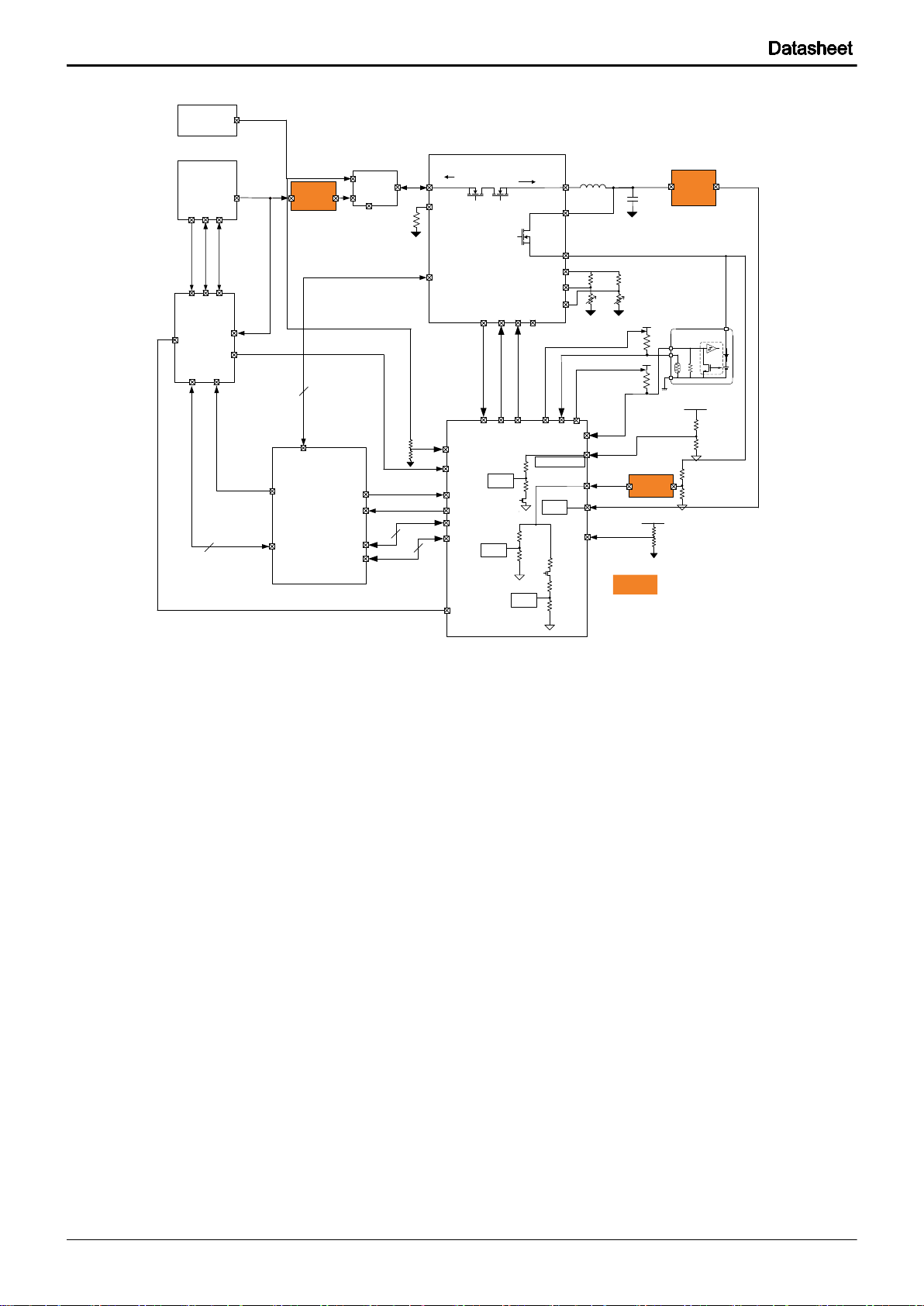
TSZ02201-BD2610GW-1-2
2cell-Battery
Charger
VBUS
SW
SYS
BAT
1.2 A max
when in
VOTG boost
mode
VCHG
15m
Ħ
max
VBUS
VLV 2 SOC
I2C _2
GPIOz
LCHR
VSYS_A
/CE
I2C
SVID
VUSBPHY
I2C
SVID
USB PHY
VBUS
VBAT
CHGDET #
ID D+ D-
RST#
ULPI
12
2
3
AC Adapter
Micro -AB
connector
ID D+ D -
VBUS
VAC
VDC
Power
Select
2
I2C
VREFT
ILIM
TS 1
ILI M1
ULPI
TS 2
4A max in
charging
mode
VBUS
REGN
ILI M0
CHGDET_B
ILI M0
ILI M1
VDCIN
VDCIN
BATID
VUSBPHY
VDC
VBUS
CH
GRINT _BINT
VBATSENSE
NTC NTC
R
BSI
0~130kΩ
Digital
Battery
Communication
Battery Pack
t°
VREFB
All VSYS
BATIDIN
BATIDOUT
Buffer
Buck
Converter
Boost
Converter
VSYS_B
R
R
Added Device
VSYSSENSE(A2sample-name)
I2CM_SZ(A1sample-name)
VSYS_A
R=178kΩ
R=1500kΩ
R=500kΩ
R=196kΩ
BCU
BATDET
R=6000kΩ
R=2000kΩ
BATMON
R=125kΩ
R=100kΩ
R=25kΩ
UVLO
OVP
BPTH ER M
VRE F
B
VRE F
T
Fig. 1-3 2-cell battery system
9/305
BD2610GW
© 2012 ROHM Co., Ltd. All rights reserved.
www.rohm.com
TSZ22111・15・001
TSZ02201-BD2610GW-1-2
5V AC/DC
ADAPTER
USB
POWER
BATTERY
PACK
POWER
MUX
CHARGER
VOLTAGE
REGULATORS
BD2610GW
I2C
VDDQ_VTT
SVID
I2C
SVID
VCC
VNN
V1P0A
V1P0S
V1P05S
VDDQ
VREFDQ0
V1P2SX
V1P8A
V1P8U
V1P8SX
VREFT
V3P3A
V3P3U
V3P3S
VUSBPHY
VSDIO
V2P85S
V2P85SX
V5P0S
VBUS
VHOST
VHDMI
VSYS_U
VSYS_S
VSYS_SX
V1P2A
INPUT PWER
DETECTION
& CONTROL
ADC
SEQUENCING
STATE
MACHINE
SOC + Platform
Devices
PUSH
BUTTON
DET
PWM
& GPIO
DISPLAY
BACKLIGHT
GP SYSTEM
CONTROL
SENSORS
VDCIN
VBUS
VBATSENSE
VSYS1
RSMRST_B
PLTRST_B
SLP_S0IX_B
SLP_S3_B
SLP_S4_B
SUSPWRDNACK
PWRBTNIN_B
GPIO1P0_UIBTN_B
PWRBTN_B
VSYS
VREF25
Backup
Battery
Charger
VRTC
VREFDQ1
V1P0SX
V1P2S
V1P8S
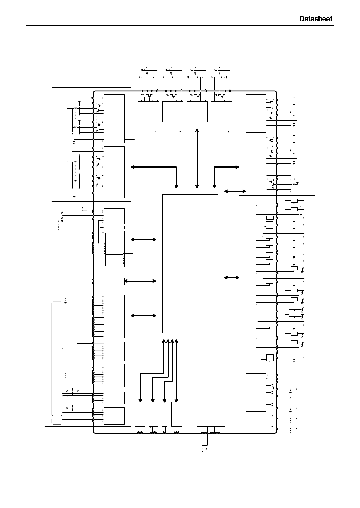
1-2 Simplified Block Diagram
Fig. 1-4 Simplified Block Diagram
10/305

BD2610GW
© 2012 ROHM Co., Ltd. All rights reserved.
www.rohm.com
TSZ22111・15・001
TSZ02201-BD2610GW-1-2
PCB Layout 1 (TBD)
1-3 Recommended Component PCB Layout
Fig. 1-5 PCB Layout (Height: 1.0mm)
11/305

BD2610GW
© 2012 ROHM Co., Ltd. All rights reserved.
www.rohm.com
TSZ22111・15・001
TSZ02201-BD2610GW-1-2
BOM List 1 (TBD)
1-4 BOM List
Table. 1-1 BOM List (1)
12/305

BD2610GW
© 2012 ROHM Co., Ltd. All rights reserved.
www.rohm.com
TSZ22111・15・001
TSZ02201-BD2610GW-1-2
BOM List 2 (TBD)
Table. 1-2 BOM List (2)
13/305
BD2610GW
© 2012 ROHM Co., Ltd. All rights reserved.
www.rohm.com
TSZ22111・15・001
TSZ02201-BD2610GW-1-2
0
1
2
3
4
5
6
0 25 50 75 100 125 150
Power Dissipation [W]
Ambient Temperature [°C]
P
DMAX
=5.1W
θja = 24.4 °C/W
ROHM2610
Lot No.
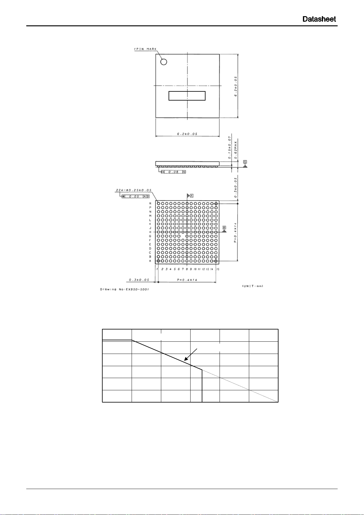
1-5 Package Dimension (corresponded with rev0.98; 2.4 Package )
Fig. 1-6 Package Dimension (Tentative)
1-5-1 Thermal Derating Curve
* 41mW/C is de-rated under the temperature of 25°C or higher. The value is with the test subject mounted on 170mm x 180mm x
1.6mm (Glass epoxy FR-4 PCB). The data is a simulated reference data, therefore, ROHM Co. ,Ltd. assumes no responsibility or
liability whatsoever for any damages resulting from the unusual or unexpected operation, such as neglect/improper installation,
alteration, or accident arising from improper handling,.
Fig. 1-7 Thermal Derating Curve
14/305

BD2610GW
© 2012 ROHM Co., Ltd. All rights reserved.
www.rohm.com
TSZ22111・15・001
TSZ02201-BD2610GW-1-2
1 2 3 4 5 6 7 8 9
10
11
12
13
14
15 A
DEBUG
_SVID
_CLK
DEBUG
_SVID
_ALERT
_B
VNN
_LX3
VNN
_VIN3
VNN
_LX4
VNN
_GND4
V1P8A
_GND
V1P8A
_LX
V1P8A
_VIN
V1P2SX
_VIN
VDDQ
_VIN0
VDDQ
_LX0
VDDQ
_GND0
T4
T5
A
B
DEBUG
_SVID
_DATA
T9
VNN
_GND3
BCU
DISA
VNN
_VIN4
VREFD
Q0
V1P8SX
V1P8S
_VIN
V1P8S
V1P2SX
VDDQ
_VIN1
VDDQ
_LX1
VDDQ
_GND1
T3
T7
B
C
VNN
_LX2
VNN
_GND2
VNN
_GND23
GND3
GPIO1
VDD
VREFD
Q1
V1P2A
V1P8U
_FB
V1P8A
_FBP
V1P2S
VDDQ
_VTT
_VIN
VDDQ
_VTT
VDDQ
_VTT
_GND
VDDQ
_VTT
_FB
V2P85S
C
D
VNN
_VIN2
SDMMC
3_PWR
_EN_B
VNN_C
OMP
PWR
BTN_B
BCU
DISCRIT
PWM2
ILIM0
ILIM1
VREF25
_2
V1P8U
_EN_B
VDDQ
_VTT
_R
VDDQ
_FBP
GND2
V2P85S
_LX1
V2P85S
_GND
D
E
VNN
_LX1
VNN
_VIN1
VBAT
BKUP
SVID
_CLK
BCU
DISB
PWM1
GPIO1
P0_UI
BTN_B
VDCIN
VBUS
GPIO1
P5
GPIO1
P7
VSYS
_SX
_EN_B
V2P85S
_FBP
V2P85S
_LX0
V2P85S
_VIN
E
F
VNN
_GND1
VNN
_FBP
GND4
SVID
_DIO
SVID
_ALERT
_B
PWM0
GPIO1
P1
GPIO1
P2
GPIO1
P3
VSYS_U
_EN_B
V3P3U
_EN_B
V3P3A
_FBP
V2P85S
X
_VIN
V2P85S
X
V3P3A_
0
F
G
VSDIO
_V1P8A
_VIN
VSDIO
VSDIO
_V3P3A
_VIN
VCC
_FBN
BACK
LIGHT
_EN
SDWN
_B
GPIO1
P6
GPIO1
P4
VSYS
_SX
_FB
VSYS_U
_FB
V3P3U
_FB
V3P3S
_FB
V3P3A_1 V3P3A
_LX11
G
H
VNN
_LX0
VNN
_VIN0
VSYS1
BAT
LOW_B
ACP
RESENT
PANEL
_EN
RTC
_POR
SDMMC
3
_1P8
_EN
GPIO0
P7
VBUS
_EN
VHOST
_EN
V3P3S
_EN_B
VUSB
PHY
V3P3A
_LX10
V3P3A
_GND
H
J
VNN
_GND0
VCC
_FBP
VREF25
_1
RSM
RST_B
VCCAP
WROK
IRQ
THERM
TRIP_B
PWR
BTN
IN_B
GPIO0
P6
GPIO0
P5
GPIO0
P2
VSYS_S
GPIO0
VDD
V3P3A
_LX00
V3P3A
_LX01
J
K
VCC
_GND0
MODEM
_OFF_B
DRAM
PWROK
CORE
PWROK
PLT
RST_B
PRO
CHOT_B
SLP_
S4_B
SYS
THERM0
VBAT
SENSE
GPIO0
P4
GPIO0
P1_BAT
IDOUT
V1P0SX
_FB
VSYS2
V3P3A
_VIN1
V3P3A
_VIN0
K
L
VCC
_LX0
VCC
_VIN0
SLP
_S0IX_B
SUSPW
R
DNACK
SLP
_S3_B
ULPI
_VBUS
_EN
SYS
THERM1
SYS
THERM2
BP
THERM1
GPIO0
P3
GPIO0
P0_BAT
IDIN
V1P0S
_FB
VHDMI
_VIN
V5P0S0
V5P0S1
L
M
VCC
_VIN1
CHG
RINT_B
VCC
_COMP
I2C
_VIO
I2C
_CLK
I2C
_DATA
BATID
VREFB
BP
THERM0
V1P0A
_FBP
V1P0S
_EN
V5P0S
_FBP
VHDMI
V5P0S
_LX0
V5P0S
_LX1
M
N
VCC
_LX1
VCC
_GND1
VCC
_GND12
I2CM
_CLK
I2CM
_DATA
ADC
VDD
VREFT
GND5
VREF25
_0
GND0
V1P0SX
_EN
GND1
VLP
V5P0S
_GND0
V5P0S
_GND1
N
P
DEBUG
_I2C
_DATA
T8
VCC
_GND2
CHG
DET_B
VCC
_VIN3
VCC
_GND34
VCC
_GND4
V1P05S
_FBP
VSYSSE
NSE
V1P05S
_LX
V1P0A
_VIN1
V1P0A
_LX1
V1P0A
_GND1
T2
T6
P
R
DEBUG
_I2C
_CLK
DEBUG
_CS
VCC
_LX2
VCC
_VIN2
VCC
_LX3
VCC
_GND3
VCC
_LX4
VCC
_VIN4
V1P05S
_GND
V1P05S
_VIN
V1P0A
_VIN0
V1P0A
_LX0
V1P0A
_GND0
T0
T1
R 1 2 3 4 5 6 7 8 9
10
11
12
13
14
15
1-6 Ball Configuration
<TOP VIEW>
Fig. 1-8 Ball Configuration
15/305
BD2610GW
© 2012 ROHM Co., Ltd. All rights reserved.
www.rohm.com
TSZ22111・15・001
TSZ02201-BD2610GW-1-2
PMIC
Subsystem
BALL
#
Pin Name
Dir.
Pin Description
Voltage
Level
Terminal
Equivalent
Circuit
VCC
L2
VCC_VIN0
I
VCC input
VSYS
A
M1
VCC_VIN1
R4
VCC_VIN2
P5
VCC_VIN3
R8
VCC_VIN4
K1
VCC_GND0
I
VCC ground
0V
A
N2
VCC_GND1
N3
VCC_GND12
P3
VCC_GND2
R6
VCC_GND3
P6
VCC_GND34
P7
VCC_GND4
L1
VCC_LX0
O
VCC switch node
VSYS
A
N1
VCC_LX1
R3
VCC_LX2
R5
VCC_LX3
R7
VCC_LX4
J2
VCC_FBP
I
VCC feedback sense positive
VCC
B
G4
VCC_FBN
I
VCC/VNN feedback sense negative
0V B M3
VCC_COMP
O
VCC compensation
VREF25
C
VNN
H2
VNN_VIN0
I
VNN input
VSYS
A
E2
VNN_VIN1
D1
VNN_VIN2
A4
VNN_VIN3
B5
VNN_VIN4
J1
VNN_GND0
I
VNN ground
0V
A
F1
VNN_GND1
C2
VNN_GND2
C3
VNN_GND23
B3
VNN_GND3
A6
VNN_GND4
H1
VNN_LX0
O
VNN switch node
VSYS
A
E1
VNN_LX1
C1
VNN_LX2
A3
VNN_LX3
A5
VNN_LX4
F2
VNN_FBP
I
VNN feedback sense positive
VNN
B
D3
VNN_COMP
I
VNN compensation
VREF25
C
V1P0A
R11
V1P0A_VIN0
I
V1P0A input
VSYS
A
P11
V1P0A_VIN1
R13
V1P0A_GND0
I
V1P0A ground
0V
A
P13
V1P0A_GND1
R12
V1P0A_LX0
O
V1P0A switch node
VSYS
A
P12
V1P0A_LX1
M10
V1P0A_FB
I
V1P0A feedback sense positive
V1P0A
D
V1P05S
R10
V1P05S_VIN
I
V1P05S input
VSYS
A
P10
V1P05S_LX
O
V1P05S switch node
VSYS
A
R9
V1P05S_GND
I
V1P05S ground
0V A P8
V1P05S_FBP
I
V1P05S feedback sense positive
V1P05S
D
1-7 Ball List (corresponded with rev0.98; 2.3 Pin List)
Table. 1-3 Ball List (1)
16/305
BD2610GW
© 2012 ROHM Co., Ltd. All rights reserved.
www.rohm.com
TSZ22111・15・001
TSZ02201-BD2610GW-1-2
PMIC
Subsystem
BALL
#
Pin Name
Dir.
Pin Description
Voltage
Level
Terminal
Equivalent
Circuit
VDDQ
A11
VDDQ_VIN0
I
VDDQ input
VSYS
A
B11
VDDQ_VIN1
A13
VDDQ_GND0
I
VDDQ ground
0V
A
B13
VDDQ_GND1
A12
VDDQ_LX0
O
VDDQ switch node
VSYS
A
B12
VDDQ_LX1
D12
VDDQ_FBP
I
VDDQ feedback sense positive
VDDQ
D
V1P8A
A9
V1P8A_VIN
I
V1P8A input
VSYS
A
A7
V1P8A_GND
I
V1P8A ground
0V
A
A8
V1P8A_LX
O
V1P8A switch node
VSYS
A
C9
V1P8A_FBP
I
V1P8A feedback sense positive
V1P8A
D
V2P85S
E15
V2P85S_VIN
I
V2P85S input
VSYS
A
E14
V2P85S_LX0
O
V2P85S switch node connection
VSYS
A
D14
V2P85S_LX1
O
V2P85S switch node connection
V2P85S
E
D15
V2P85S_GND
I
V2P85S ground
0V
A
C15
V2P85S
O
V2P85S output
V2P85S
BS
E13
V2P85S_FBP
I
V2P85S feedback sense positive
V2P85S
F
V3P3A
K15
V3P3A_VIN0
I
V3P3A input
VSYS
A
K14
V3P3A_VIN1
J14
V3P3A_LX00
O
V3P3A switch node
VSYS
A
J15
V3P3A_LX01
H14
V3P3A_LX10
O
V3P3A switch node
V3P3A
E
G15
V3P3A_LX11
H15
V3P3A_GND
I
V3P3A ground
0V
A
F15
V3P3A_0
O
V3P3A output
V3P3A
BS
G14
V3P3A_1
F12
V3P3A_FBP
I
V3P3A feedback sense positive
V3P3A
F
V5P0S
M14
V5P0S_LX0
I
V5P0S switch node
VSYS
H
M15
V5P0S_LX1
N14
V5P0S_GND0
I
V5P0S ground
0V
H
N15
V5P0S_GND1
L14
V5P0S0
O
V5P0S output
V5P0S
H
L15
V5P0S1
M12
V5P0S_FBP
I
V5P0S feedback sense positive
V5P0S
F
VSDIO
G3
VSDIO
_V3P3A_VIN
I
VSDIO input for V3P3A
V3P3A
J
G2
VSDIO
O
VSDIO output
VSDIO
J
G1
VSDIO
_V1P8A_VIN
I
VSDIO input for V1P8A
V1P8A
J
VDDQ_VTT
C11
VDDQ_VTT_VIN
I
VDDQ_VTT input
V1P0A
K
C12
VDDQ_VTT
O
VDDQ_VTT output
VDDQ
_VTT
K
C14
VDDQ_VTT_FB
I
VDDQ_VTT feedback
VDDQ
_VTT
K
D11
VDDQ_VTT_R
I
VDDQ_VTT reference voltage
VDDQ
BB
C13
VDDQ_VTT_GND
I
VDDQ_VTT ground
0V
K
VUSBPHY
H13
VUSBPHY
O
VUSBPHY output
VUSB
PHY
L
V1P8U
D10
V1P8U_EN_B
O
V1P8U enable signal
V1P8A
M
C8
V1P8U_FB
I
V1P8U sense
V1P8U
BL
V1P8S
B9
V1P8S
O
V1P8S output
V1P8S
BM
B8
V1P8S_VIN
I
V1P8S/V1P8SX input
V1P8A
BM
V1P8SX
B7
V1P8SX
O
V1P8SX output
V1P8SX
P
Table. 1-4 Ball List (2)
17/305
BD2610GW
© 2012 ROHM Co., Ltd. All rights reserved.
www.rohm.com
TSZ22111・15・001
TSZ02201-BD2610GW-1-2
PMIC
Subsystem
BALL
#
Pin Name
Dir.
Pin Description
Voltage
Level
Terminal
Equivalent
Circuit
VREFDQ0
B6
VREFDQ0
O
VREFDQ0 output
VREFDQ
R
VREFDQ1
C6
VREFDQ1
O
VREFDQ1 output
VREFDQ
R
V1P2A
C7
V1P2A
O
V1P2A output
V1P2A R V1P2S
C10
V1P2S
O
V1P2S output
V1P2S
BM
V1P2SX
B10
V1P2SX
O
V1P2SX output
V1P2SX
BM
A10
V1P2SX_VIN
I
V1P2SX / V1P2S input
VDDQ
BM
V3P3U
F11
V3P3U_EN_B
O
V3P3U enable signal
V3P3A
S
G12
V3P3U_FB
I
V3P3U sense
V3P3U
BP
V3P3S
H12
V3P3S_EN_B
O
V3P3S enable signal
V3P3A
BN
G13
V3P3S_FB
I
V3P3S sense
V3P3S
BR
V1P0S
M11
V1P0S_EN
O
V1P0S enable signal
V5P0S
T
L12
V1P0S_FB
I
V1P0S sense
V1P0S
BL
V1P0SX
N11
V1P0SX_EN
O
V1P0SX enable signal
V5P0S
T
K12
V1P0SX_FB
I
V1P0SX sense
V1P0SX
BL
VHOST
H11
VHOST_EN
O
VHOST enable signal
V5P0S
T
VBUS
H10
VBUS_EN
O
VBUS enable signal
V5P0S
T
L6
ULPI_VBUS_EN
I
VBUS current limit enable signal
VSYS
V
VHDMI
M13
VHDMI
O
VHDMI output
VHDMI
W
L13
VHDMI_VIN
I
VHDMI input
V5P0S
W
V2P85SX
F14
V2P85SX
O
V2P85SX output
V2P85SX
P
F13
V2P85SX_VIN
I
V2P85SX input
V2P85S
P
VSYS_U
F10
VSYS_U_EN_B
O
VSYS_U enable signal
VSYS
X
G11
VSYS_U_FB
I
VSYS_U sense
VSYS_U
N
VSYS_S
J12
VSYS_S
O
VSYS_S output
VSYS_S
Y
VSYS_SX
E12
VSYS_SX_EN_B
O
VSYS_SX enable signal
VSYS
X
G10
VSYS_SX_FB
I
VSYS_SX sense
VSYS
_SX
N
VSYS
H3
VSYS1
I
PMIC input power for internal supply,
also used for VSYS sense
VSYS
-
K13
VSYS2
I
PMIC input power for internal supply
VSYS
-
SVID
E4
SVID_CLK
I
Serial VID clock from Valleyview2
V1P0S
Z
F4
SVID_DIO
I/O
Serial VID data in & out
V1P0S
Z
F5
SVID_ALERT_B
O
Serial VID interrupt from PMIC to
Vallyview2
V1P0S
Z
Power Source
Detection
and Charger
Control
E8
VDCIN
I
AC/DC adapter voltage input detection.
5V
AA
E9
VBUS
I
USB voltage input detection.
5V
AA
P4
CHGDET_B
I
USB DCP detection from USBPHY
(0=USB DCP/CDP/ACA)
VSYS
AB
M2
CHGRINT_B
I
Battery charging status and fault indicator
from charging IC. 0=charging in progress,
1=charging completed,
mid-level=charger fault
VSYS
AC
D7
ILIM0
O
Limits charging current which varies
depending on power sources (AC
adapter, USB DCP/CDP/ACA, USB SDP)
VSYS
X
D8
ILIM1
Table. 1-5 Ball List (3)
18/305

BD2610GW
© 2012 ROHM Co., Ltd. All rights reserved.
www.rohm.com
TSZ22111・15・001
TSZ02201-BD2610GW-1-2
PMIC
Subsystem
BALL
#
Pin Name
Dir.
Pin Description
Voltage
Level
Terminal
Equivalent
Circuit
System Control
- Reset,
Power,
and Control
Signals
M5
I2C_CLK
I
I2C clock. Slave.
V1P8S
AD
M6
I2C_DATA
I/O
I2C data, slave.
V1P8S
AE
N4
I2CM_CLK
O
I2C clock, master.
VREF25
AF
N5
I2CM_DATA
I/O
I2C data, master.
VREF25
AG
P9
VSYSSENSE
I
Battery voltage detection for 2CELL
VSYS
V
M4
I2C_VIO
I
Input power for I2C slave
V1P8S
AD
J8
PWRBTNIN_B
I
System power button input
VSYS
AH
D4
PWRBTN_B
O
System power button output
V1P8A
AJ
K5
PLTRST_B
I
Reset signal from SOC to PMIC
V1P8A
AK
L3
SLP_S0IX_B
I
Standby S0ix trigger from SOC, 0=enter
S0ix. 1=exit S0ix
V1P8A
AK
L5
SLP_S3_B
I
Sleep S3 trigger from SOC, 0=enter S3.
1=exit S3
V1P8A
AK
K7
SLP_S4_B
I
Sleep S4 trigger from SOC, 0=enter S4.
1=exit S4
V1P8A
AK
J4
RSMRST_B
O
Resume reset output to SOC,
de-asserted (=1) after V3P3A
V3P3A
AL
K3
DRAMPWROK
O
Output to SOC, asserted (=1) after
VDDQ is up and stable.
VDDQ
AM
J5
VCCAPWROK
O
Output from PMIC to SOC for DDR
VDDQ
AM
K4
COREPWROK
O
Power Good signal to SOC after core
VRs are valid
V3P3A
AL
L4
SUSPWRDNACK
I
Signal from SOC. In junction with
assertion of SLP_S4_B, it inform the
PMIC to turn off SUS and enter SOC
mechanical OFF state
V1P8A
AK
H5
ACPRESENT
O
AC adapter is plugged in with valid
voltage
V1P8A
AJ
H4
BATLOW_B
O
Indicate to SOC that battery voltage is
not sufficiently high to boot IA
V1P8A
AJ
J6
IRQ
O
Interrupt to SOC
V1P8A
AJ
J7
THERMTRIP_B
I
Catastrophic thermal event indicator to
PMIC to shut off all power rails (active
low)
V1P8A
AN
K6
PROCHOT_B
O
Output (open drain) to SOC to limit SOC
power in a thermal event
V1P0S
AP
H8
SDMMC3_1P8_EN
I
1.8V/3.3V selection for SD card, 0=3.3V,
1=1.8V
V1P8S
AR
D2
SDMMC3_PWR
_EN_B
I
SD card power enable, default 1=OFF
V1P8S
AR
K2
MODEM_OFF_B
O
Modem Hard Reset Signal
V1P8A
AJ
G6
SDWN_B
O
PMIC indication of imminent system
shutdown or SIM Card Removal (active
low)
V1P8A
AJ
H7
RTC_POR
I
Power on reset for PMIC from platform
signal RTEST_B
VBAT
BKUP
BE
GPIO0(LV)
L11
GPIO0P0_BATIDIN
I/O
GPIO (default) than can be alternatively
configured as battery ID input from the
SOC for digital BIF support
GPIO0V
DD
AS
K11
GPIO0P1
_BATIDOUT
I/O
GPIO (default) than can be alternatively
configured as battery ID output from the
SOC for digital BIF support
GPIO0V
DD
J11
GPIO0P2
I/O
Low voltage general purpose I/O pins
GPIO0V
DD
L10
GPIO0P3
K10
GPIO0P4
J10
GPIO0P5
J9
GPIO0P6
H9
GPIO0P7
J13
GPIO0VDD
I
Low voltage GPIO supply
V1P8A
AT
Table. 1-6 Ball List (4)
19/305
BD2610GW
© 2012 ROHM Co., Ltd. All rights reserved.
www.rohm.com
TSZ22111・15・001
TSZ02201-BD2610GW-1-2
PMIC
Subsystem
BALL
#
Pin Name
Dir.
Pin Description
Voltage
Level
Terminal
Equivalent
Circuit
GPIO1(HV)
E7
GPIO1P0_UIBTN_B
I/O
GPIO (default) that can alternatively use
as a Utility Button for Power Button
quantifier gating platform power down
GPIO1V
DD
AV
F7
GPIO1P1
I/O
High Voltage General Purpose I/O pins
GPIO1V
DD
F8
GPIO1P2
F9
GPIO1P3
G9
GPIO1P4
E10
GPIO1P5
G8
GPIO1P6
E11
GPIO1P7
C5
GPIO1VDD
I
High Voltage GPIO supply
V3P3A/V
SYS
AW
BCU
B4
BCUDISA
O
BCU Warning Zone A output disable
signal
V1P8A
AJ
E5
BCUDISB
O
BCU Warning Zone B output disable
signal
V1P8A
AJ
D5
BCUDISCRIT
O
BCU Critical Zone output disable signal
V1P8A
AJ
PWM
F6
PWM0
O
Pulse Width Modulated output control
signals
V1P8A
AJ
E6
PWM1
AJ
D6
PWM2
AJ
Display
Panel Control
G5
BACKLIGHT_EN
O
Backlight enable
V3P3A
AX
H6
PANEL_EN
O
LCD panel enable
V3P3A
AX
GPADC
N6
ADCVDD
I
Input power to ADC, dedicated pin for
routing and placement
VREF25
AY
K8
SYSTHERM0
I
System temperature thermistor input
SYSTHERM0, …, SYSTHERM2 for ADC
VREFT
AZ
L7
SYSTHERM1
AZ
L8
SYSTHERM2
AZ
M9
BPTHERM0
I
Battery temperature input of pack 0 for
GPADC input and charger disable
VREFT
AZ
L9
BPTHERM1
I
Battery temperature input of pack 1 for
GPADC input and charger disable
VREFT
AZ
M7
BATID
I
Battery identification from battery - for
battery presence detection and battery
size indication
VREFB
BA
K9
VBATSENSE
I
Battery voltage sense
VBAT
BB
MISC
M8
VREFB
O
Battery ID bias voltage
VREFB
BC
N7
VREFT
O
battery thermistor, and system
thermistor's bias voltage
VREFT
BC
E3
VBATBKUP
I
Coin cell backup battery connection
VBAT
BKUP
BD
A1
DEBUG_SVID_CLK
I
Serial VID clock from Valleyview2, debug
channel
V1P0S
Z
B1
DEBUG_SVID
_DATA
I/O
Serial VID data in & out, debug channel
V1P0S
Z
A2
DEBUG_SVID
_ALERT_B
O
Serial VID interrupt from PMIC, debug
channel
V1P0S
Z
R1
DEBUG_I2C_CLK
I
I2C clock, slave, debug channel
I2CVIO
AD
P1
DEBUG_I2C_DATA
I/O
I2C data, slave, debug channel
I2CVIO
AE
R2
DEBUG_CS
I
Interrupt, debug channel
VSYS
BF
N13
VLP
I
Logic Power Supply
VREF25
BG
N9
VREF25_0
I
Power source for internal Circuit
BG
J3
VREF25_1
O
LDO Output for internal Circuit
BH
D9
VREF25_2
I
Power source for internal Circuit
BG
Table. 1-7 Ball List (5)
20/305
BD2610GW
© 2012 ROHM Co., Ltd. All rights reserved.
www.rohm.com
TSZ22111・15・001
TSZ02201-BD2610GW-1-2
PMIC
Subsystem
BALL
#
Pin Name
Dir.
Pin Description
Voltage
Level
Terminal
Equivalent
Circuit
MISC
N10
GND0
I
Substrate Ground
0V
-
N12
GND1
-
D13
GND2
-
C4
GND3
-
F3
GND4
-
N8
GND5
-
R14
T0
I
No connect balls at corner
-
BJ
R15
T1
BJ
P14
T2
BJ
B14
T3
BJ
A14
T4
BJ
A15
T5
BJ
P15
T6
I/O
BK
B15
T7
I/O
BK
P2
T8
I
BJ
B2
T9
BJ
Table. 1-8 Ball List (6)
Note:
Dir. (Pin Direction): I = Input, O = Output, I/O = Input or Output
21/305
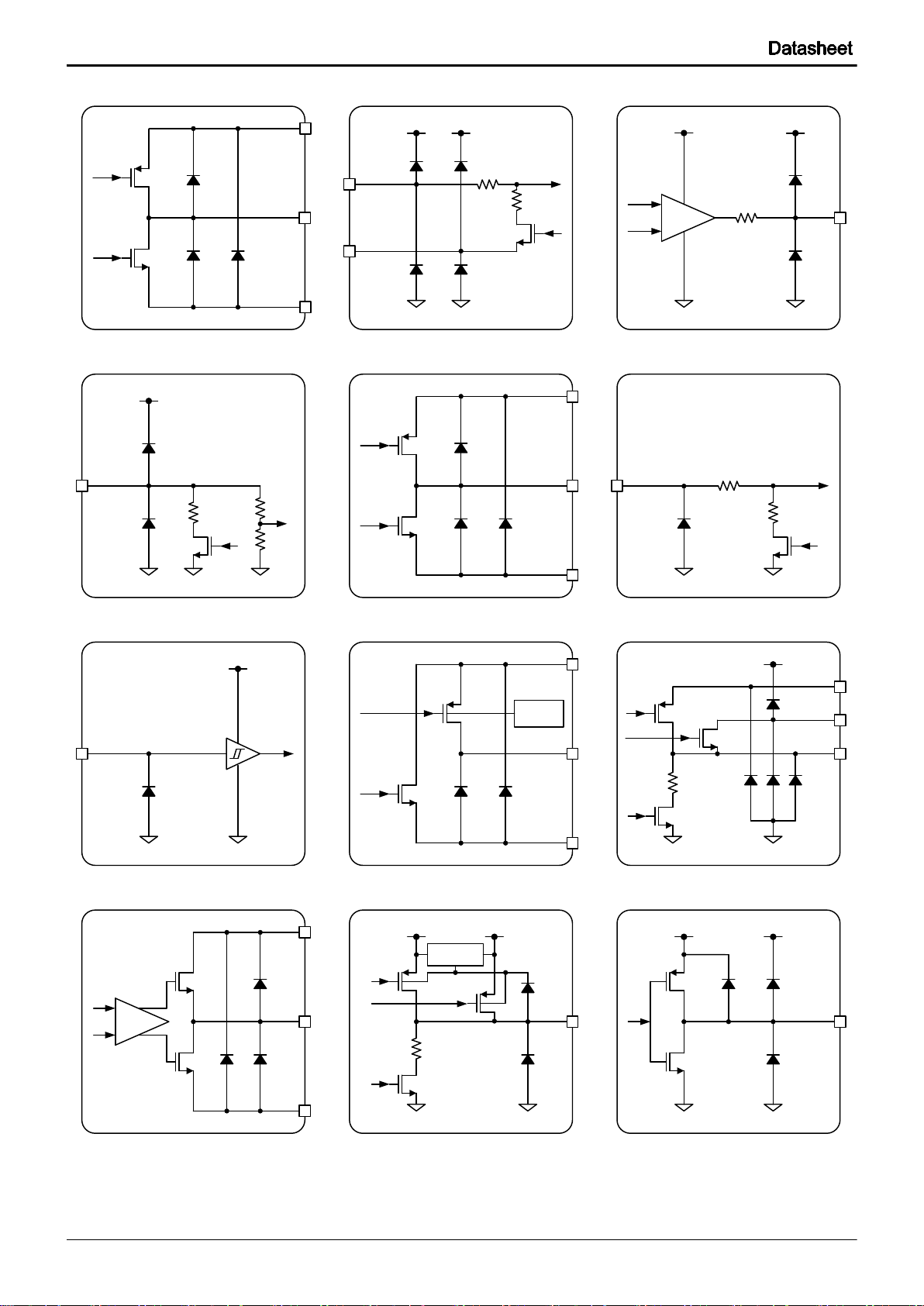
BD2610GW
© 2012 ROHM Co., Ltd. All rights reserved.
www.rohm.com
TSZ22111・15・001
TSZ02201-BD2610GW-1-2
(A)
_VIN
_LX
_GND
(B)
VSYS
GND
(C)
GND
VREF25
GND
VSYS
GND
_FBP
_FBN
VSYS
GND GND
(D)
GND GND
(F)
V1P8A
GND GND
(G)
(E)
(H) (J)
_LX
_GND
OUTPUT
_LX
_GND
OUTPUT
V3P3A
GND
GND
VSYS
V1P8A
VSDIO
(K)
_VIN
OUT
PUT
_GND
(L)
GND
GND
VSYS V3P3A
(M)
VSYS
GND
V1P8S_VIN
GND
High Select
+
-
VSYS
GND
BG
Control
+
-
-
+
Fig. 1-9 Terminal Equivalent Circuit (1)
22/305
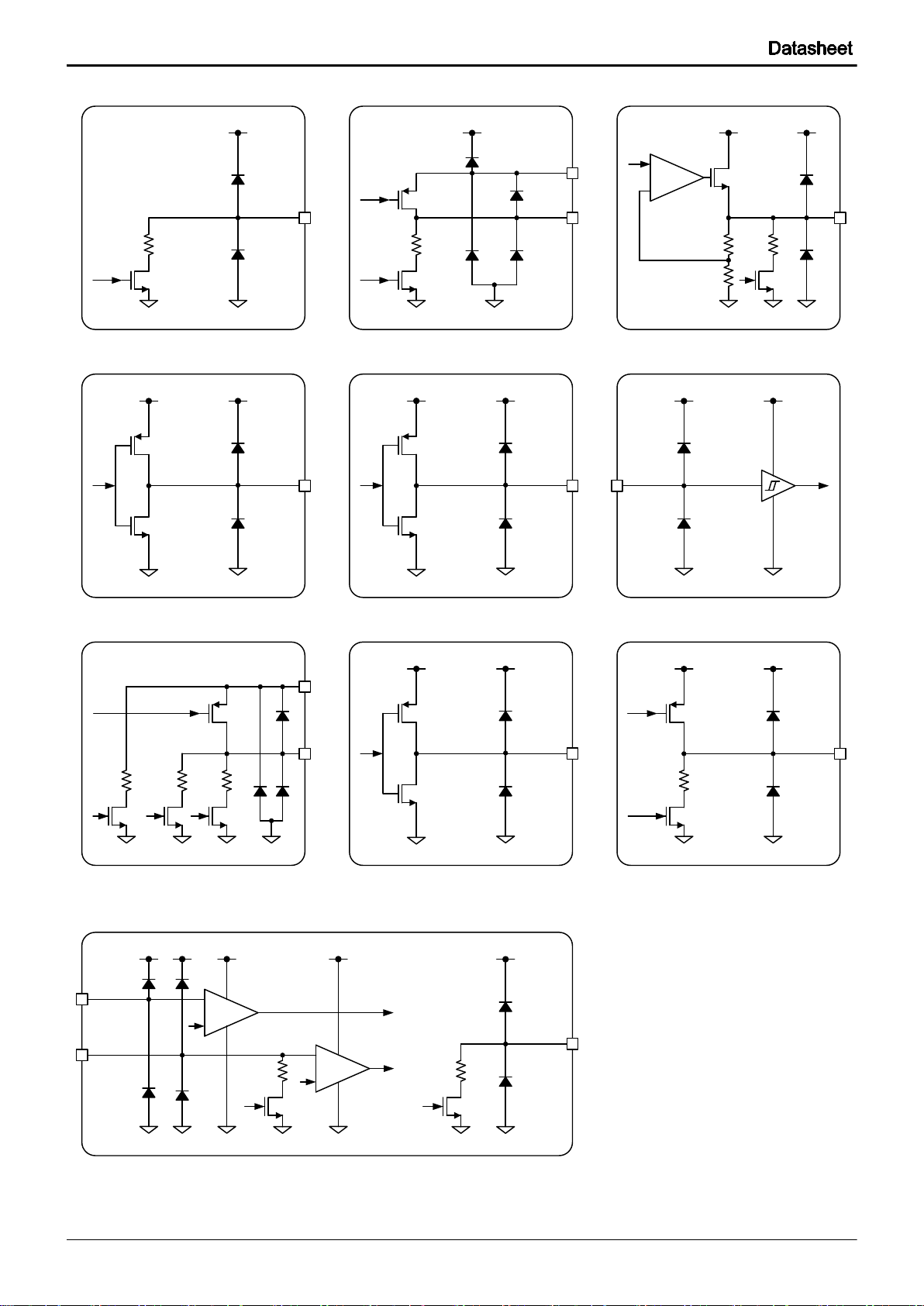
BD2610GW
© 2012 ROHM Co., Ltd. All rights reserved.
www.rohm.com
TSZ22111・15・001
TSZ02201-BD2610GW-1-2
(N) (P) (R)
GND
V1P8S_VIN
GND
V1P8S_VIN
(S)
GND
V3P3A
GND
V3P3A
(T)
GND
V5P0S
GND
V5P0S
(V)
(W)
_IN
GND
GND
OUTPUT
GNDGND
(X)
GND
VSYS
GND
VSYS
(Y)
GND
GND
VSYS VSYS
(Z)
GND
GND
VSYSVSYS
GND GND
VSYS VREF25
GND GNDGND
VREF25
ALERT_B
_CLK
_DIO
GND
+
-
+
-
+
-
VSYS
GND GND
VSYS
GND
GND
VSYS
_IN
GND
GND
VSYS
OUT
PUT
Fig. 1-10 Terminal Equivalent Circuit (2)
23/305
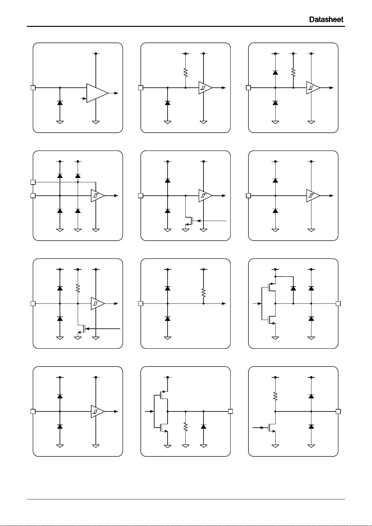
BD2610GW
© 2012 ROHM Co., Ltd. All rights reserved.
www.rohm.com
TSZ22111・15・001
TSZ02201-BD2610GW-1-2
(AA)
GND
V5P0S
GND
VSYS
GND GND
(AB)
+
-
(AC)
VSYS
GND GND
VSYS
VSYS
VSYS
GND GND
(AD)
GND
I2C_VIO
VSYS VSYS
GNDGND
I2C_VIO
GND
VREF25
GND GND
(AE)
VSYS
VSYS
GND
(AF)
GND
VREF25
GND
(AG)
GND
(AH)
VSYS VSYS
(AJ)
GND
V1P8A
GND
VSYS
V1P8A
GND GND
(AK)
VSYS
(AL) (AM)
GND
V1P2SX_VIN
GND
VSYS
GND
V3P3A
GND GND
Fig. 1-3 Terminal Equivalent Circuit (3)
24/305
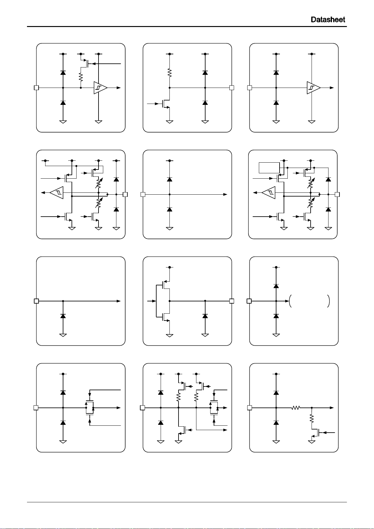
BD2610GW
© 2012 ROHM Co., Ltd. All rights reserved.
www.rohm.com
TSZ22111・15・001
TSZ02201-BD2610GW-1-2
(AN)
V1P8A
GND GND
VSYS V1P8A
(AR)
V1P8S
GND GND
VSYS
(AT)
GND
VSYS
(AW)
GND
(AX)
GND
V3P3A
GND
(AY)
GND
VSYS
Used for Internal
Power Source
(AZ)
GND
VSYS
(BA)
GND
VSYS
GND
VREF25 V1P8A VSYS
GND GND
(BB)
(AS)
GND
GPIO0VDD
GPIO0VDD
GND
VSYS
GND
VSYS
GND
GPIO1VDD
GPIO1VDD
GND
(AV)
BG
Control
(AP)
GND
V1P0S_FB
GND
VSYS
Fig. 1-4 Terminal Equivalent Circuit (4)
25/305
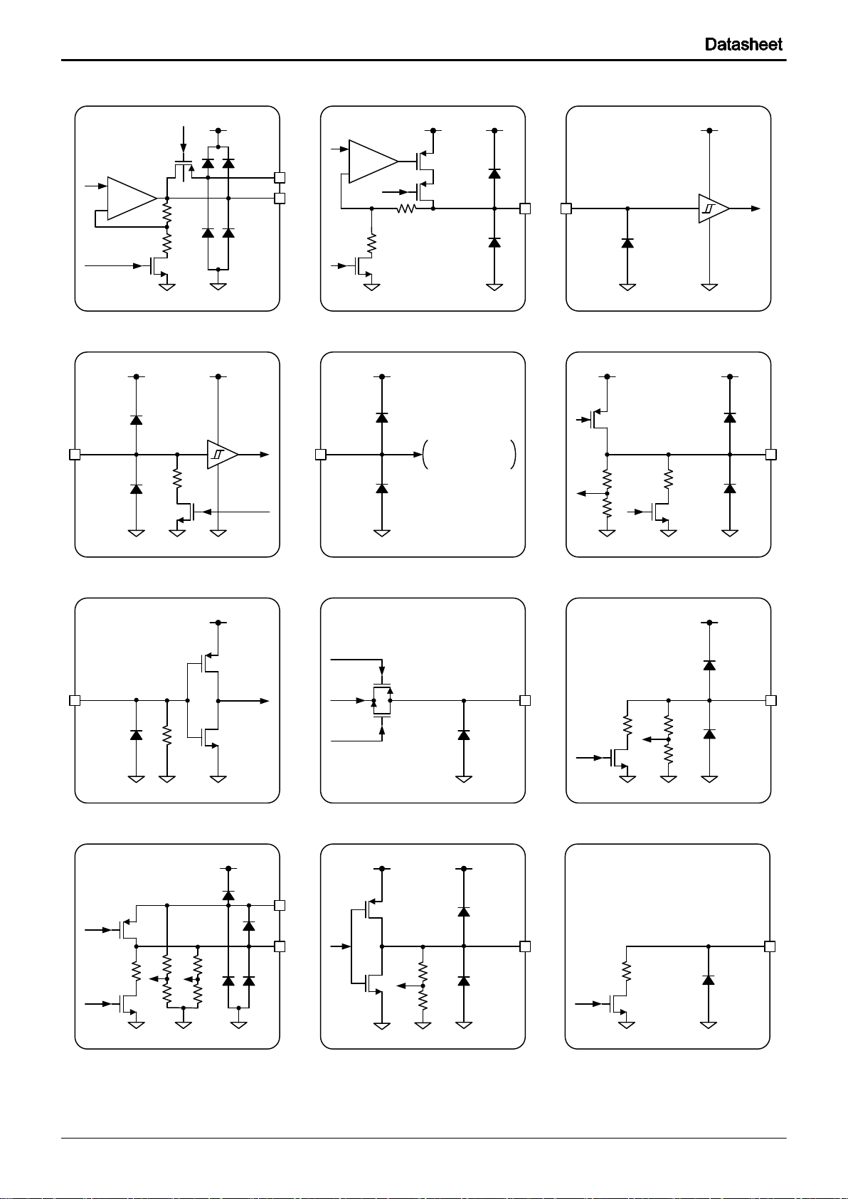
BD2610GW
© 2012 ROHM Co., Ltd. All rights reserved.
www.rohm.com
TSZ22111・15・001
TSZ02201-BD2610GW-1-2
(BC)
VREFT
VSYS
GND
VSYS
GND
VREFB
+
-
GND
VSYS
GND
VSYS
(BD)
VBATBKUP
GND GND
(BE)
+
-
VSYS
GND GND
(BF)
VSYS
GND
(BG)
GND
VSYS
Used for Internal
Power Source
(BH)
GND GND
VSYS
GND
VSYS
(BJ)
GND
VREF25
GNDGND
(BK)
GND
(BL)
(BM) (BN)
GND
V3P3A
GND
V3P3A
GND
GND
GND
VSYS
GND
_IN
GND
GND
VSYS
OUT
PUT
GND
(BP)
GND
GND
Fig. 1-5 Terminal Equivalent Circuit (5)
26/305
BD2610GW
© 2012 ROHM Co., Ltd. All rights reserved.
www.rohm.com
TSZ22111・15・001
TSZ02201-BD2610GW-1-2
(BR)
GND
GNDGND
(BS)
_LX
_GND
OUTPUT
GND
Fig. 1-6 Terminal Equivalent Circuit (6)
27/305
BD2610GW
© 2012 ROHM Co., Ltd. All rights reserved.
www.rohm.com
TSZ22111・15・001
TSZ02201-BD2610GW-1-2
PMIC
Subsystem
Parameter
Symbol
Rating
Unit
-
Storage Temperature Range
TSTG
-55 to 150
°C
GND
GNDx Voltage (GND)
GND
0
V
VSYS
VSYS1 and VSYS2 Voltage Range
(VSYS)
VSYS
-0.3 to 6.0
V
VSYS1 to VSYS2 Voltage Range
VS12
0
V
MISC
VREF25_1 Output Voltage (VREF25)
VREF25
-0.3 to 4.5
V
VREF25_0, VREF25_2 Input Voltage
VREF25I
-0.3 to 4.5
V
VREF25_1 to VREF25_0
and VREF25_2 Voltage
VR1X
-0.3 to 0.3
GND to VREFB Voltage
VREFB
-0.3 to (VREF25 + 0.3)
V
GND to VREFT Voltage
VREFT
-0.3 to (VREF25 + 0.3)
V
GND to
DEBUG_SVID_DATA
and DEBUG_SVID_ALERT_B
Voltage Range
VGIOMISC1
-0.3 to (V1P0S + 0.3)
V
GND to
DEBUG_I2C_CLK and DEBUG_I2C_DATA
Voltage Range
VGIOMISC2
-0.3 to (V1P8S + 0.3)
V
GND to
T0, T1, T2, T3, T4, T5,T8 and T9
Voltage Range
TESTIN
-0.3 to (VSYS + 0.3)
V
GND to
T6and T7 Voltage Range
TESTO
-0.3 to (VSYS + 0.3)
V
VCC
VCC_GNDx Voltage
VGVCC
GND
V
VCC_VINx Voltage
VIVCC
VSYS
V
VCC_GNDx to VCC_LXx
Voltage Range
VGLVCC
-1.0 to (VSYS + 1.0)
V
VCC_GNDx to VCC_FBx
Voltage Range
VGINVCC
-0.3 to (VREF25 + 0.3)
V
VCC_GNDx to VCC_COMP
Voltage Range
VGOVCC
-0.3 to (VREF25 + 0.3)
V
VNN
VNN_GNDx Voltage
VGVNN
GND
V
VNN_VINx Voltage
VIVNN
VSYS
V
VNN_GNDx to VNN_LXx
Voltage Range
VGLVNN
-1.0 to (VSYS + 1.0)
V
VNN_GNDx to VNN_FBP
Voltage Range
VGINVNN
-0.3 to (VREF25 + 0.3)
V
VNN_GNDx to VNN_COMP
Voltage Range
VGOVNN
-0.3 to (VREF25 + 0.3)
V
2 Electrical Characteristics
This chapter describes detailed analog electrical characteristics such as absolute maximum ratings, operating ratings,
voltage rails, current consumption.
2-1 Absolute Maximum Ratings (corresponded with rev0.98; 2.5.1 Operational Ratings)
Table. 2-1 Absolute Maximum Ratings (1)
28/305
BD2610GW
© 2012 ROHM Co., Ltd. All rights reserved.
www.rohm.com
TSZ22111・15・001
TSZ02201-BD2610GW-1-2
PMIC
Subsystem
Parameter
Symbol
Rating
Unit
V1P0A
V1P0A_GNDx Voltage
VGV10A
GND
V
V1P0A_VINx Voltage
VIV10A
VSYS
V
V1P0A_GNDx to V1P0A_LXx
Voltage Range
VGLV10A
-1.0 to (VSYS + 1.0)
V
V1P0A_GNDx to V1P0A_FBP
Voltage Range
VGINV10A
-0.3 to (VREF25 + 0.3)
V
V1P05S
V1P05S_GND Voltage
VGV105S
GND
V
V1P05S_VIN Voltage
VIV105S
VSYS
V
V1P05S_GND to V1P05S_LX
Voltage Range
VGLV105S
-1.0 to (VSYS + 1.0)
V
V1P05S_GND to V105S_FBP
Voltage Range
VGINV105S
-0.3 to (VREF25 + 0.3)
V
VDDQ
VDDQ_GNDx Voltage
VGVDDQ
GND
V
VDDQ_VINx Voltage
VIVDDQ
VSYS
V
VDDQ_GNDx to VDDQ_LXx
Voltage Range
VGLVDDQ
-1.0 to (VSYS + 1.0)
V
VDDQ_GNDx to VDDQ_FBP
Voltage Range
VGINVDDQ
-0.3 to (VREF25 + 0.3)
V
V1P8A
V1P8A_GND Voltage
VGV18A
GND
V
V1P8A_VIN Voltage
VIV18A
VSYS
V
V1P8A_GND to V1P8A_LX
Voltage Range
VGLV18A
-1.0 to (VSYS + 1.0)
V
V1P8A_GND to V1P8A_FBP
Voltage Range
VGINV18A
-0.3 to (VREF25 + 0.3)
V
V2P85S
V2P85S_GNDx Voltage
VGV285S
GND
V
V2P85S_VINx Voltage
VIV285S
VSYS
V
V2P85S_GND to V2P85S_LXx
Voltage Range
VGLV285S
-1.0 to 7.0
V
V2P85S_GND to V2P8S_FBP
Voltage Range
VGINV285S
-0.3 to 7.0
V
V2P85S_GND to V2P85S
Voltage Range
VGOV285S
-0.3 to 7.0
V
V3P3A
V3P3A_GND Voltage
VGV33A
GND
V
V3P3A_VINx Voltage
VIV33A
VSYS
V
V3P3A_GND to V3P3A_LXx
Voltage Range
VGLV33A
-1.0 to 7.0
V
V3P3A_GND to V3P3A_FBP
Voltage Range
VGINV33A
-0.3 to 7.0
V
V3P3A_GND to V3P3A_x Voltage Range
VGOV33A
-0.3 to 7.0
V
V5P0S
V5P0S_GNDx Voltage
VGV50S
GND
V
V5P0S_GNDx to V5P0S_LXx
Voltage Range
VGLV50S
-1.0 to 7.0
V
V5P0S_GNDx to V5P0S_FBP
Voltage Range
VGINV50S
-0.3 to 7.0
V
V5P0S_GNDx to V5P0Sx Voltage Range
VGOV50S
-0.3 to 7.0
V
VSDIO
VSDIO_3P3A_VIN Voltage
VI3VSDIO
V3P3A
V
VSDIO_1P8A_VIN Voltage
VI2VSDIO
V1P8A
V
GND to VSDIO Voltage Range
VGOVSDIO
-0.3 to ((V3P3A or V1P8A) + 0.3)
V
Table. 2-2 Absolute Maximum Ratings (2)
29/305

BD2610GW
© 2012 ROHM Co., Ltd. All rights reserved.
www.rohm.com
TSZ22111・15・001
TSZ02201-BD2610GW-1-2
PMIC
Subsystem
Parameter
Symbol
Rating
Unit
VDDQ_VTT
VDDQ_VTT_GND Voltage
VGVQT
GND
V
VDDQ_VTT_VIN Voltage
VIVQT
V1P0A
V
VDDQ_VTT_R Voltage
VRVQT
VDDQ
V
VDDQ_VTT_GND to VDDQ_VTT_FB
Voltage Range
VGINVQT
-0.3 to (VREF25 + 0.3)
V
VDDQ_VTT_GND to VDDQ_VTT
Voltage Range
VGOVQT
-0.3 to (V1P0A + 0.3)
V
VUSBPHY
GND to VUSBPHY Voltage Range
VGOVUP
-0.3 to ((V3P3A or VSYS) + 0.3)
V
V1P8U
GND to V1P8U_FB Voltage Range
VGINV18U
-0.3 to (VREF25 + 0.3)
V
GND to V1P8U_EN_B Voltage Range
VGOV18U
-0.3 to (V1P8A + 0.3)
V
V1P8S
/ V1P8SX
V1P8S_VIN Voltage
VGINV18S
V1P8A
V
GND to V1P8S and V1P8SX Voltage Range
VGOV18S
-0.3 to (V1P8A + 0.3)
V
VREFDQ
GND to VREFDQx Voltage Range
VGOVRDQ
-0.3 to (V1P8A + 0.3)
V
V1P2A
GND to V1P2A Voltage Range
VGOV12A
-0.3 to (V1P8A + 0.3)
V
V1P2S
/ VSFR
V1P2SX_VIN Voltage
V12S
V1P2A
V
GND to
V1P2S and V1P2SX Voltage Range
VGOV12S
-0.3 to (V1P2A + 0.3)
V
V3P3U
GND to V3P3U_FB Voltage Range
VGINV33U
-0.3 to (V3P3A + 0.3)
V
GND to V3P3U_EN_B Voltage Range
VGOV33U
-0.3 to (V3P3A + 0.3)
V
V3P3S
GND to V3P3S_FB Voltage Range
VGINV33S
-0.3 to (V3P3A + 0.3)
V
GND to V3P3S_EN_B Voltage Range
VGOV33S
-0.3 to (V3P3A + 0.3)
V
V1P0S
GND to V1P0S_FB Voltage Range
VGINV10S
-0.3 to (VREF25 + 0.3)
V
GND to V1P0S_EN_B Voltage Range
VGOV10S
-0.3 to (V5P0S + 0.3)
V
V1P0SX
GND to V1P0SX_FB Voltage Range
VGINV10SX
-0.3 to (VREF25 + 0.3)
V
GND to V1P0SX_EN_B Voltage Range
VGOV10SX
-0.3 to (V5P0S + 0.3)
V
VHOST
GND to VHOST_EN Voltage Range
VGOVHOST
-0.3 to (V5P0S + 0.3)
V
VBUS
GND to ULPI_VBUS_EN Voltage Range
VGINBUS
-0.3 to (VSYS + 0.3)
V
GND to VBUS_EN Voltage Range
VGOVBUS
-0.3 to (V5P0S + 0.3)
V
VHDMI
VHDMI_VIN Voltage
VHDMI
V5P0S
V
GND to VHDMI Voltage Range
VGOHDMI
-0.3 to 6.0
V
V2P85SX
V2P85SX_VIN Voltage
V285SX
V2P85S
V
GND to V2P85SX Voltage Range
VGOV285SX
-0.3 to (V2P85S + 0.3)
V
VSYS_U
GND to VSYS_U_SENSE
Voltage Range
VGINVSYSU
-0.3 to (VSYS + 0.3)
V
GND to VSYS_U_EN_B
Voltage Range
VGOVSYSU
-0.3 to (VSYS + 0.3)
V
VSYS_S
GND to VSYS_S Voltage Range
VGOVSYSS
-0.3 to (VSYS + 0.3)
V
VSYS_SX
GND to VSYS_SX_SENSE
Voltage Range
VGINVSYSSX
-0.3 to (VSYS + 0.3)
V
GND to VSYS_SX_EN_B
Voltage Range
VGOVSYSSX
-0.3 to (VSYS + 0.3)
V
VLP
VLP Voltage
VLP
VREF25
V
SVID
GND to
SVID_CLK and SVID_DIO Voltage Range
VGINSVID
-0.3 to (V1P0A + 0.3)
V
GND to SVID_ALERT_B Voltage Range
VGOSVID
-0.3 to (V1P0A + 0.3)
V
Power
Source
Detect
GND to VDCIN and VBUS Voltage Range
VGINPS1
-0.3 to 6.0V
V
GND to CHGDET_B Voltage Range
VGINPS2
-0.3 to (VSYS + 0.3)
V
GND to CHGRINT_B Voltage Range
VGINPS3
-0.3 to (VSYS + 0.3)
V
GND to ILIMx Voltage Range
VGOPS
-0.3 to (VSYS + 0.3)
V
Table. 2-3 Absolute Maximum Ratings (3)
30/305

BD2610GW
© 2012 ROHM Co., Ltd. All rights reserved.
www.rohm.com
TSZ22111・15・001
TSZ02201-BD2610GW-1-2
PMIC
Subsystem
Parameter
Symbol
Rating
Unit
System
Control
I2C_VIO Voltage
VI2C1
V1P8S
V
GND to
I2C_CLK, I2C_DATA, SDMMC3_1P8_EN
and SDMMC3_PWR_EN_B
Voltage Range
VGIO1
-0.3 to (V1P8S + 0.3)
V
GND to
PWRBTN_B, PLTRST_B,
SLP_S0IX_B, SLP_S3_B,
SLP_S4_B, SUSPWRDNACK,
ACPRESENT, BATLOW_B,
IRQ, THERMTRIP_B,
MODEM_OFF_B and SDWN_B
Voltage Range
VGIO2
-0.3 to (V1P8A + 0.3)
V
GND to I2CM_CLK
and I2CM_DATA Voltage Range
VI2C2
-0.3 to (VREF25 + 0.3)
V
GND to PWRBTNIN_B
And VSYSSENSE Voltage Range
VGIO3
-0.3 to (VSYS + 0.3)
V
GND to DRAMPWROK
and VCCAPWROK Voltage Range
VGIO4
-0.3 to (VDDQ + 0.3)
V
GND to RSMRST_B, COREPWROK
and RTC_POR Voltage Range
VGIO5
-0.3 to (V3P3A + 0.3)
V
GND to PROCHOT_B Voltage Range
VGIO6
-0.3 to (V1P0S + 0.3)
V
GPIO0
GPIO0VDD Voltage
VGPIO0
V1P8A
V
GND to
GPIO0P0_BATIDIN, GPIO0P1_BATINOUT,
and GPIO0Px Voltage Range
VGIOGP0
-0.3 to (VSYS + 0.3)
V
GPIO1
GPIO1VDD Voltage
VGPIO1
V3P3A
V
GND to
GPIO1P0_UIBTN_B and GPIO1Px
Voltage Range
VGIOGP1
-0.3 to ((VSYS or GPIO1VDD) + 0.3)
V
BCU
GND to
BCUDISA, BCUDISB and BCUDISCRIT
Voltage Range
VGIOBCU
-0.3 to (V1P8S + 0.3)
V
PWM
GND to PWMx Voltage Range
VGIOPWM
-0.3 to (V1P8S + 0.3)
V
Display
GND to
BACKLIGHT_EN and PANEL_EN
Voltage Range
VGIOD
-0.3 to (V3P3A + 0.3)
V
GPADC
ADCVDD Voltage
VADC
VREF25
V
GND to VBATSENSE
VGINADC1
-0.3 to 6.0
V
GND to
BATID, BPTHERMx and SYSTHERMx
Voltage Range
VGINADC2
-0.3 to (VREF25 + 0.3)
V
ESD
Human Body Model
HMB
±1000
V
Charged Device Model
CDM
±500
V
Parameter
Symbol
Limit
Unit
Min.
Typ.
Max.
VSYS Supply Voltage
VSYS
2.7
3.6
5.25
V
Operating Temperature Range
TOPR
-30
25
85
℃
Table. 2-4 Absolute Maximum Ratings (4)
2-2 Operating Ratings (corresponded with rev0.98; 3.2 System Power Map)
Table. 2-5 Operating Ratings
31/305

BD2610GW
© 2012 ROHM Co., Ltd. All rights reserved.
www.rohm.com
TSZ22111・15・001
TSZ02201-BD2610GW-1-2
Voltage Rail
Type
Input
Voltage
Default Output
Voltage [V]
VCC
SVID buck
VSYS
0.500~1.200
VNN
SVID buck
VSYS
0.500~1.200
V1P0A
Buck
VSYS
1.010
V1P05S
Buck
VSYS
1.050
V1P8A
Buck
VSYS
1.817
VDDQ
Buck
VSYS
1.240
V3P3A
Buck-boost
VSYS
3.332
V2P85S
Buck-boost
VSYS
2.900
V5P0S
Boost
VSYS
5.048
VSDIO
FET Switches
V1P8A
1.817
V3P3A
3.332
VDDQ_VTT
Linear VR
V1P0A
0.620
V1P2A
Linear VR
V1P8A
1.200
VREFDQ0
Linear VR
V1P8A
0.600~1.220
VREFDQ1
Linear VR
V1P8A
0.600~1.220
VREFT/VREFB
Linear VR
VSYS
2.000
VUSBPHY
FET Switches
VSYS
VSYS
V3P3A
3.332
VSYS_S
FET Switch
VSYS
VSYS
V1P2S
FET Switch
VDDQ
1.240
V1P2SX
FET Switch
VDDQ
1.240
V1P8S
FET Switch
V1P8A
1.817
V1P8SX
FET Switch
V1P8A
1.817
V2P85SX
FET Switch
V2P85S
2.900
VHDMI
FET Switch
V5P0S
5.048
2-3 Voltage Rails Description
BD2610GW incorporates 6 buck regulators (including 2 SVID buck regulators), 2 buck-boost regulators, 1 boost regulator, 4
linear regulators, and 9 sets of FET switches. Each voltage rail output is described in Table. 2-6. The system power map is
shown in Fig. 2-1.
Table. 2-6 Voltage Rails Output Voltage List (corresponded with rev0.98; 3.3 Voltage Rails Requirement)
32/305

BD2610GW
© 2012 ROHM Co., Ltd. All rights reserved.
www.rohm.com
TSZ22111・15・001
TSZ02201-BD2610GW-1-2
5V AC/DC
ADAPTER
USB
POWER
BATTERY
PACK
(1SxP)
POWER
MUX
CHARGER
VSYS_S
INPUT PWER
DETECTION
& CONTROL
PUSH BUTTON
DETECTION
VDCIN
VBUS
VBATSENSE
VSYS1
PWRBTNIN_B
GPIO1P0_UIBTN_B
PWRBTN_B
FET Switch
FET Switch
FET Switch
Linear VR
(VREFT)
FET Switch
VREFT
5.0V
Boost
(V5P0S)
FET Switch
FET Switch
FET Switch
V5P0S
VBUS
VHOST
VHDMI
2.85V
Buck Boost
(V2P85S)
FET Switch
V2P85S
V2P85SX
3.3V
Buck Boost
(V3P3A)
FET Switch
FET Switch
FET Switch
FET
Switches
FET
Switches
1.8V
Buck
(V1P8A)
V3P3A
V3P3U
V3P3S
VUSBPHY
VSDIO
V3P3IFP
FET Switch
Linear VR
(VREFDQ1)
FET Switch
FET Switch
Linear VR
(V1P2A)
V1P8A
V1P8U
VREFDQ0
V1P2A
V1P8S
V1P8SX
SVID
Buck
(VCC)
SVID
Buck
(VNN)
VCC
VNN
FET Switch
FET Switch
VDDQ
V1P2S
V1P2SX
1.24V
Buck
(VDDQ)
Linear VR
Sink / Source
(VDDQ_VTT)
1.0V
Buck
(V1P0A)
VDDQ_VTT
V1P0A
FET Switch
FET Switch
V1P0S
V1P0SX
1.05V
Buck
(V1P05S)
V1P05S
SEQUENCING
STATE
MACHINE
RSMRST_B
PLTRST_B
SLP_S0IX_B
SLP_S3_B
SLP_S4_B
SUSPWRDNACK
PWM
& GPIO
DISPLAY BACKLIGHT &
GP SYSTEM CONTROL
IRQ
ADC
SENSORS (8 Channels)
CURRENT MONITOR (5 Channels)
SVID I/F
SVID_ALERT#
SVID_CLK
SVID_DIO
I2C
(Slave)
I2C_SCL
I2C_SDA
FET Switch
FET Switch VSYS_U
VSYS_SX
VSYS
CRYSTAL COVE PMIC
POWER RAILS
ON in S4
ON in S3
ON in S0ix
ON in S0
3V Li
VRTC
Linear VR
(VREF25)
*Internal VR
Backup
Battery
Charger
Linear VR
(VREFDQ0)
VREFDQ1
Fig. 2-1 System Power Map (corresponded with rev0.98; 3.2 System Power Map: Figure 3-1)
33/305

BD2610GW
© 2012 ROHM Co., Ltd. All rights reserved.
www.rohm.com
TSZ22111・15・001
TSZ02201-BD2610GW-1-2
No.
Voltage Rail
Type
Max Current
[mA]
Over Current
Protection [mA]
Over Voltage
Protection [V]
OCP, OVP
IRQ
1
VCC
SVID buck
8000
> 10400
Table. 2-8
Support
2
VNN
SVID buck
8000
> 10400
Table. 2-8
Support
3
V1P0A
Buck
1900
> 2470
1.430
None
4
V1P05S
Buck
900
> 1170
1.502
None
5
V1P8A
Buck
1627
> 2115.1
2.574
None
6
VDDQ
Buck
2800
> 3640
1.95
None
7
V3P3A
Buck-boost
1569
> 2039.7
4.719
None
8
V2P85S
Buck-boost
550
> 715*3
4.290
None
9
V5P0S
Boost
955
> 1241.5
6.500
None
10
VSDIO
FET Switch(1.8V)
200
None
None
None
FET Switch(3.3V)
400
None
None
None
11
VDDQ_VTT
Linear VR
325
> 422.5
None
None
12
V1P2A
Linear VR
30
> 39
None
None
13
VREFT
Linear VR
1
> 2.6
None
None
14
VUSBPHY
FET Switch(3.3V)
40
None
None
None
FET Switch(VSYS)
40
None
None
None
15
VSYS_U
Ext FET Switch
2750
None
None*2
None
16
VSYS_S
FET Switch
10
None
None*2
None
17
V1P2S
FET Switch
34
None
None
None
18
V1P2SX
FET Switch
155
None
None
None
19
V1P8S
FET Switch
144
None
None
None
20
V1P8SX
FET Switch
240
None
None
None
21
V2P85SX
FET Switch
250
None
None
None
22
V3P3U
Ext FET Switch
700
None
None
None
23
VHDMI
FET Switch
55
> 71.5
None
None
24
V1P8U
Ext FET Switch
355
None
None
None
25
V1P0S
Ext FET Switch
410
None
None
None
26
V1P0SX
Ext FET Switch
916
None
None
None
27
V3P3S
Ext FET Switch
584
None
None
None
28
VHOST
Ext FET Switch
900
None
None
None
29
VBUS
Ext FET Switch
900
None
None
None
30
VSYS_SX
Ext FET Switch
2500
None
None*2
None
31
VREFDQ0
Linear VR
10
> 13
None
None
32
VREFDQ1
Linear VR
10
> 13
None
None
2-3-1 Voltage Rails - Maximum current and Protection
The maximum current is shown below. Every voltage rail has integrated over current protection (OCP) function. If the output
current exceeds the OCP threshold and fold back, it will limit the current to protect the BD2610GW from heat and damage.
Then VCC and VNN buck regulators, buck-boost regulators, a boost regulator, and VSYS_S switch has over voltage
protection (OVP) function. If the output voltage exceeds the OVP threshold by voltage droop and voltage overshoot, the
voltage rail turn off to protect from devices damage.
And some OCP and OVP give the interrupt request (refer to 3: Control of Voltage Rails).
Table. 2-7 Voltage Rails I
(corresponded with rev0.98; 3.3.1 Voltage Rails Imax Specification and 3.3.4.1 Over Voltage Protection )
and Protection Function List
MAX
*1 These parameters are reference data without pre-shipping inspection.
*2 VSYS has the over voltage protection >5.4V.
*3 V2P85S supports 850mA peak output current while 5μs. 715mA output more than 5μs is not supported.
34/305

BD2610GW
© 2012 ROHM Co., Ltd. All rights reserved.
www.rohm.com
TSZ22111・15・001
TSZ02201-BD2610GW-1-2
Vout max
VCC,VNN[V]
OVP[V]
VID7
VID6
VID5
VID4
VID3
VID2
VID1
VID0
x 0 x x x x x x ~1.2
1.40
1 1 0 0 0 x x x 1.21~1.24
1.44
1 1 0 0 1 x x x 1.25~1.28
1.48
1 1 0 1 0 x x x 1.29~1.32
1.52
1 1 0 1 1 x x x 1.33~1.36
1.56
1 1 1 0 0 x x x 1.37~1.40
1.60
1 1 1 0 1 x x x 1.41~1.44
1.64
1 1 1 1 0 x x x 1.45~1.48
1.68
1 1 1 1 1 x x x 1.49~1.52
1.72
Table. 2-8 Voltage Rails I
and Protection Function List
MAX
35/305

BD2610GW
© 2012 ROHM Co., Ltd. All rights reserved.
www.rohm.com
TSZ22111・15・001
TSZ02201-BD2610GW-1-2
No.
Voltage Rail
Type
SOC S0
SOC S0IX
SOC S3
SOC S4
SOC G3
1
VCC
SVID buck
ON
ON
OFF
OFF
OFF
2
VNN
SVID buck
ON
ON
OFF
OFF
OFF
3
V1P0A
Buck
ON
ON
ON
ON
OFF
4
V1P05S
Buck
ON
ON
OFF
OFF
OFF
5
V1P8A
Buck
ON
ON
ON
ON
OFF
6
VDDQ
Buck
ON
ON
ON
OFF
OFF
7
V3P3A
Buck-boost
ON
ON
ON
ON
OFF
8
V2P85S
Buck-boost
ON
ON
OFF
OFF
OFF
9
V5P0S
Boost
ON
ON
WON*
WON*
WON*
10
VSDIO
FET Switches
ON/OFF
ON/OFF
OFF
OFF
OFF
11
VDDQ_VTT
Linear VR
ON
ON/OFF
OFF
OFF
OFF
12
V1P2A
Linear VR
ON
ON
ON
ON
OFF
13
VREFT
Linear VR
Control by ADC
14
VUSBPHY
FET Switch
ON
ON
ON
ON
ON
15
VSYS_U
Ext FET Switch
ON/OFF
ON/OFF
ON/OFF
OFF
OFF
16
VSYS_S
FET Switch
ON/OFF
ON/OFF
OFF
OFF
OFF
17
V1P2S
FET Switch
ON
ON
OFF
OFF
OFF
18
V1P2SX
FET Switch
ON
OFF
OFF
OFF
OFF
19
V1P8S
FET Switch
ON
ON
OFF
OFF
OFF
20
V1P8SX
FET Switch
ON/OFF
ON/OFF
OFF
OFF
OFF
21
V2P85SX
FET Switch
ON/OFF
ON/OFF
OFF
OFF
OFF
22
V3P3U
Ext FET Switch
ON/OFF
ON/OFF
ON/OFF
OFF
OFF
23
VHDMI
FET Switch
ON/OFF
ON/OFF
OFF
OFF
OFF
24
V1P8U
Ext FET Switch
ON
ON
ON
OFF
OFF
25
V1P0S
Ext FET Switch
ON
ON
OFF
OFF
OFF
26
V1P0SX
Ext FET Switch
ON
OFF
OFF
OFF
OFF
27
V3P3S
Ext FET Switch
ON
ON
OFF
OFF
OFF
28
VHOST
Ext FET Switch
ON/OFF
ON/OFF
OFF
OFF
OFF
29
VBUS
Ext FET Switch
ON/OFF
ON/OFF
OFF
OFF
OFF
30
VSYS_SX
Ext FET Switch
ON/OFF
ON/OFF
OFF
OFF
OFF
31
VREFDQ0
Linear VR
ON
ON
ON
OFF
OFF
32
VREFDQ1
Linear VR
ON
ON
ON
OFF
OFF
2-4 Current Consumption
Voltage rails ON/OFF for respective power states are shown below.
Table. 2-9 Voltage Rails ON/OFF for respective power states
(corresponded with_rev0.98; 3.3.2 Voltage Rail ON/OFF at various power state)
*The voltage at “WON” is “VSYS – VF (VF is internal parasitic diode)”.
The current consumption of each state is shown below.
36/305

BD2610GW
© 2012 ROHM Co., Ltd. All rights reserved.
www.rohm.com
TSZ22111・15・001
TSZ02201-BD2610GW-1-2
Parameter
Symbol
Target Spec.
Unit
Remarks
Min.
Typ.
Max.
SOC G3 Current
Consumption
IDDG3
-
35
60
μA
SOC S4 Current
Consumption
IDDS4
-
650 - μA
SOC S3 Current
Consumption
IDDS3
-
750 - μA
SOC S0IX Current
Consumption
IDDS0IX
-
1.6 - mA
SOC S0 (PS0) Current
Consumption
IDDS0P0
-
TBD - mA
SOC S0 (PS2) Current
Consumption
IDDS0P2
-
TBD - mA
SOC S0 (PS3) Current
Consumption
IDDS0P3
-
TBD - mA
GPADC Conversion Current
IDDAD
-
0.6 - mA
BATID
Conversion,
fS=25kHz
Table. 2-10 Current Consumption
Unless otherwise specified,
Ta = 25C, VSYS = 3.6V, GND=0V, No Load
37/305

BD2610GW
© 2012 ROHM Co., Ltd. All rights reserved.
www.rohm.com
TSZ22111・15・001
TSZ02201-BD2610GW-1-2
VCC_VIN0
VCC_LX0
VCC_GND0
L
X0
1.0μH
C
IN0
4.7 μF
VSYS
GND
Switch
Control
+
-
Current
Sense0
C
L
352μF
(22μF x 16)
VCC
VCC_FBP
VCC_FBN
VCC_COMP
VCC_VIN1
VCC_LX1
VCC_GND1
L
X1
0.47μH
C
IN1
4.7 μF
VSYS
GND
Switch
Control
+
-
Current
Sense1
VCC_VIN2
VCC_LX2
VCC_GND2
L
X2
0.47μH
C
IN2
4.7 μF
VSYS
GND
Switch
Control
+
-
Current
Sense2
VCC_VIN3
VCC_LX3
VCC_GND3
L
X3
0.47μH
C
IN3
4.7 μF
VSYS
GND
Switch
Control
+
-
Current
Sense3
VCC_VIN4
VCC_LX4
VCC_GND4
L
X4
0.47μH
C
IN4
4.7 μF
VSYS
GND
Switch
Control
+
-
Current
Sense4
+
-
GND
SVID
GND
C
0
47pF
Phase
Shift
OSC
5
VCLK
VDIO
VCC_GND12
GND
VCC_GND34
GND
2-5 Details of Analog Electrical Characteristics
2-5-1 VCC (corresponded with_rev0.98; 3.5.1 VCC )
VCC is a high-efficiency 5 Multi-Phase buck regulator with integrated FET that converts the VSYS voltage to a regulated
voltage. This voltage regulator can dynamically change its output voltage setting using the SVID interface. VCC output
voltage range is from 0.5V to 1.2V (10mV/ step). The output voltage slew rate while ramping up/down for SVID-fast and
SVID-slow can be programmed through the VCC slew rate register (refer to 3-3-2).
Chapter 3-3 explains concerned registers and how to control VCC.
2-5-1-1 VCC Block Diagram (corresponded with_rev0.98; 3.5.1.2 VCC Block Diagram )
Fig. 2-2 VCC Block Diagram
38/305

BD2610GW
© 2012 ROHM Co., Ltd. All rights reserved.
www.rohm.com
TSZ22111・15・001
TSZ02201-BD2610GW-1-2
Parameter
Symbol
Target Spec.
Unit
Remarks
Min.
Typ.
Max.
Switching Frequency 1
f
SW1_VCC
-
3.0
-
MHz
PS0 State
Switching Frequency 2
f
SW2_VCC
-
2.0
-
MHz
PS2 State
Output Voltage VID=1.0V
V
O_VCC
0.990
1.000
1.010
V
PWM mode
Ripple Voltage 1*1
V
RP1_VCC
- 5 20
mV
P-P
PFM mode, I
OUT
= 1 mA
Ripple Voltage 2*1
V
RP2_VCC
- 1 20
mV
P-P
PWM mode, I
OUT
= 8 A
Transient Droop Voltage 1*1*2
V
DRP1_VCC
- - 40
mV
PS0 state, TR = 200ns,
I
OUT
= 1000mA to 8000mA
Transient Droop Voltage 2*1*2
V
DRP2_VCC
- - 40
mV
PS0 state, TR = 200ns,
I
OUT
= 25mA to 7000mA
Transient Overshoot Voltage 1*1*2
V
OVS1_VCC
- - 40
mV
PS0 state, TF = 200ns,
I
OUT
= 8000mA to 1000mA
Transient Overshoot Voltage 2*1*2
V
OVS2_VCC
- - 40
mV
PS0 state, TF = 200ns,
I
OUT
= 7000mA to 25mA
Maximum Output Current*1
I
MAX_VCC
8000 - -
mA
Efficiency 1*1
Eff
1_VCC
-
78 - %
PS0 State, VID = 0.7V,
I
OUT
= 100mA
Efficiency 2*1
Eff
2_VCC
-
78 - %
PS0 State, VID = 0.7V,
I
OUT
=1.5A
Efficiency 3*1
Eff
3_VCC
-
78 - %
PS0 State, VID = 0.7V,
I
OUT
= 4.5A
Efficiency 4*1
Eff
4_VCC
-
68 - %
PS0 State, VID = 0.7V,
I
OUT
= 8.0A
Efficiency 5*1
Eff
5_VCC
-
82 - %
PS0 State, VID = 1.0V,
I
OUT
= 100mA
Efficiency 6*1
Eff
6_VCC
-
81 - %
PS0 State, VID = 1.0V,
I
OUT
= 1.5A
Efficiency 7*1
Eff
7_VCC
-
81 - %
PS0 State, VID = 1.0V,
I
OUT
= 4.5A
Efficiency 8*1
Eff
8_VCC
-
71 - %
PS0 State, VID = 1.0V,
I
OUT
= 8.0A
Efficiency 9*1
Eff
9_VCC
-
73 - %
PS2 State, VID = 0.7V,
I
OUT
= 1mA
Efficiency 10*1
Eff
10_VCC
-
83 - %
PS2 State, VID = 0.7V,
I
OUT
= 10mA
Efficiency 11*1
Eff
11_VCC
-
83 - %
PS2 State, VID = 0.7V,
I
OUT
= 100mA
Switch PMOS ON Resistance
R
ONP_VCC
-
147
-
mΩ
Switch NMOS ON Resistance
R
ONN_VCC
-
66 - mΩ
Minimum Load Capacitance
C
LMIN_VCC
229 - -
μF
Under shoot voltage
(VDRP)
VOUT
Over shoot voltage
(VOVS)
Vrip1max
Vrip1max
Vrip1ave
Vrip2max
Vrip2max
Vrip2Ave
Vover
Vunder
Ioutmin
Ioutmax
“VDRP” = ”Vunder” - “Vrip1ave”, “VOVS” = ”Vover” - “Vrip2ave”
The definition of over-shoot and under-shoot voltage of all DC/DC is following formulas.
2-5-1-2 VCC Electrical Characteristics
(corresponded with rev0.98; 3.3.4 Voltage Rails Tolerance, 3.3.1 Voltage Rails Imax Specification, 3.3.3 Load transient
current, 3.5.1 VCC, 3.5.14 Efficiency Target )
Table. 2-11 VCC Electrical Characteristics
Unless otherwise specified,
Ta = 25C, VCC_VINx = 3.6V, VCC_GNDx = 0V, VID = 1.0V setting, PS0 State, CL = 352F, LXx=0.47H, C
C0 =47pF
= 4.7 F,
INx
*1 These parameters are reference data without pre-shipping inspection.
*2 Include ripple voltage and load regulation.
39/305

BD2610GW
© 2012 ROHM Co., Ltd. All rights reserved.
www.rohm.com
TSZ22111・15・001
TSZ02201-BD2610GW-1-2
2-5-1-3 VCC Typical Performance Curve
Unless otherwise specified,
Ta = 25C, VCC_VINx = 3.6V, VCC_GNDx = 0V, VID = 1.0V setting, PS0 state, CL = 352F, LXx=0.47H, C
C0 =47pF
= 4.7 F,
INx
Fig. 2-3 Load Regulation 1 (VID = 1.0V)
Fig. 2-5 Efficiency 1 (VID=1.0V)
Fig. 2-4 Line Regulation 1 (VID = 1.0V, I
Fig. 2-6 Ripple Voltage 1 (VID = 1.0V, I
= 8000 mA)
OUT
= 1mA)
OUT
Fig. 2-7 Ripple Voltage 2 (VID = 1.0V, I
= 8000mA)
OUT
40/305
Fig. 2-8 Load Regulation 2 (VID = 0.7V)

© 2012 ROHM Co., Ltd. All rights reserved.
www.rohm.com
TSZ22111・15・001
BD2610GW
TSZ02201-BD2610GW-1-2
Fig. 2-9 Line Regulation 2 (VID = 0.7V, I
Fig. 2-11 Load Regulation 3 (PS2 State, VID = 0.7V)
= 8000 mA)
OUT
Fig. 2-10 Efficiency 2 (VID = 0.7V)
Fig. 2-12 Line Regulation 3
(PS2 State, VID = 0.7, I
= 200 mA)
OUT
Fig. 2-13 Efficiency 3 (PS2 State, VID = 0.7V)
41/305
Fig. 2-14 Ripple Voltage
(PS2 State, VID = 0.7V, I
= 1mA)
OUT

© 2012 ROHM Co., Ltd. All rights reserved.
www.rohm.com
TSZ22111・15・001
BD2610GW
TSZ02201-BD2610GW-1-2
Fig. 2-15 Startup to Shutdown Waveform 1 (Slow mode)
Fig. 2-17 Transient Response 1 (VID = 1.0V,
I
= 25mA to 7A, TR = TF = 200ns)
OUT
Fig. 2-16 Startup to Shutdown Waveform 2 (Fast mode)
Fig. 2-18 Transient Response 2 (VID = 1.0V,
I
= 1A to 8A, TR = TF = 200ns)
OUT
Fig. 2-19 Change VID Waveform 1 (Slow mode)
42/305
Fig. 2-20 Change VID Waveform 1 (Fast mode)

© 2012 ROHM Co., Ltd. All rights reserved.
www.rohm.com
TSZ22111・15・001
BD2610GW
TSZ02201-BD2610GW-1-2
Fig. 2-21 Change state Waveform
(PS0 State to PS2 State)
Fig. 2-22 Change state Waveform
(PS2 State to PS0 State)
43/305

© 2012 ROHM Co., Ltd. All rights reserved.
www.rohm.com
TSZ22111・15・001
BD2610GW
TSZ02201-BD2610GW-1-2
L
X0
1.0μH
C
IN0
4.7 μF
VSYS
GND
Switch
Control
+
-
Current
Sense0
C
L
352μF
(22μF x 16)
VCC
L
X1
0.47μH
C
IN1
4.7 μF
VSYS
GND
Switch
Control
+
-
Current
Sense1
L
X2
0.47μH
C
IN2
4.7 μF
VSYS
GND
Switch
Control
+
-
Current
Sense2
L
X3
0.47μH
C
IN3
4.7 μF
VSYS
GND
Switch
Control
+
-
Current
Sense3
L
X4
0.47μH
C
IN4
4.7 μF
VSYS
GND
Switch
Control
+
-
Current
Sense4
+
-
GND
SVID
GND
C
0
47pF
Phase
Shift
OSC
5
VCLK
VDIO
VCC_FBN
GND
VNN_VIN0
VNN_LX0
VNN_GND0
VNN_FBP
VNN_COMP
VNN_VIN1
VNN_LX1
VNN_GND1
VNN_VIN2
VNN_LX2
VNN_GND2
VNN_VIN3
VNN_LX3
VNN_GND3
VNN_VIN4
VNN_LX4
VNN_GND4
VNN_GND23
2-5-2 VNN (corresponded with_rev0.98; 3.5.2 VNN )
VNN is a high-efficiency 5 Multi-Phase buck regulator with integrated FET that converts the VSYS voltage to a regulated
voltage. This voltage regulator can dynamically change its output voltage setting using the SVID interface. VNN output
voltage range is from 0.5V to 1.2V (10mV/ step). The output voltage slew rate while ramping up/ down for SVID-fast and
SVID-slow can be programmed through the VNN slew rate register (refer to 3-4-2).
Chapter 3-4 explains the concerned registers and how to control VCC.
2-5-2-1 VNN Block Diagram (corresponded with_rev0.98; 3.5.2.2 VNN Block Diagram )
Fig. 2-23 VNN Block Diagram
44/305

© 2012 ROHM Co., Ltd. All rights reserved.
www.rohm.com
TSZ22111・15・001
BD2610GW
TSZ02201-BD2610GW-1-2
Parameter
Symbol
Target Spec.
Unit
Remarks
Min.
Typ.
Max.
Switching Frequency 1
f
SW1_VNN
-
3.0
-
MHz
S0 State
Switching Frequency 2
f
SW2_VNN
-
2.0
-
MHz
S0IX State
Output Voltage VID=1.0V
V
O_VNN
0.990
1.000
1.010
V
PWM mode
Ripple Voltage 1*1
V
RP1_VNN
- 5 20
mV
P-P
PFM mode, I
OUT
= 1 mA
Ripple Voltage 2*1
V
RP2_VNN
- 1 20
mV
P-P
PWM mode, I
OUT
= 8 A
Transient Droop Voltage 1*1*2
V
DRP1_VNN
- - 40
mV
S0 State, TR = 200nsec
I
OUT
= 2900mA to 5600mA
Transient Droop Voltage 2*1*2
V
DRP2_VNN
- - 40
mV
S0 State, TR = 200nsec
I
OUT
= 50mA to 2750mA
Transient Overshoot Voltage 1*1*2
V
OVS1_VNN
- - 40
mV
S0 State, TF = 200nsec
I
OUT
= 5600mA to 2900mA
Transient Overshoot Voltage 2*1*2
V
OVS2_VNN
- - 40
mV
S0 State, TR = 200nsec
I
OUT
= 2750mA to 50mA
Maximum Output Current*1
I
MAX_VNN
8000 - -
mA
Efficiency 1*1
Eff
1_VNN
-
77 - %
S0 State, VID = 0.7V,
I
OUT
= 50mA
Efficiency 2*1
Eff
2_VNN
-
78 - %
S0 State, VID = 0.7V,
I
OUT
= 500mA
Efficiency 3*1
Eff
3_VNN
-
78 - %
S0 State, VID = 0.7V,
I
OUT
= 5600mA
Efficiency 4*1
Eff
3_VNN
-
68 - %
S0 State, VID = 0.7V,
I
OUT
= 8000mA
Efficiency 5*1
Eff
4_VNN
-
80 - %
S0 State, VID = 1.0V,
I
OUT
= 50mA
Efficiency 6*1
Eff
5_VNN
-
81 - %
S0 State, VID = 1.0V,
I
OUT
= 500mA
Efficiency 7*1
Eff
6_VNN
-
81 - %
S0 State, VID = 1.0V,
I
OUT
= 5600mA
Efficiency 8*1
Eff
6_VNN
-
71 - %
S0 State, VID = 1.0V,
I
OUT
= 8000mA
Efficiency 9*1
Eff
7_VNN
-
81 - %
S0IX State, VID = 0.7V,
I
OUT
= 5mA
Efficiency 10*1
Eff
8_VNN
-
83 - %
S0IX State, VID = 0.7V,
I
OUT
= 20mA
Efficiency 11*1
Eff
9_VNN
-
83 - %
S0IX State, VID = 0.7V,
I
OUT
= 100mA
Switch PMOS ON Resistance
R
ONP_VNN
-
147
-
mΩ
Switch NMOS ON Resistance
R
ONN_VNN
-
66 - mΩ
Minimum Load Capacitance
C
LMIN_VNN
229 - -
μF
2-5-2-2 VNN Electrical Characteristics
(corresponded with_rev0.98; 3.3.4 Voltage Rails Tolerance, 3.3.1 Voltage Rails Imax Specification, 3.3.3 Load
transient current, 3.5.2 VNN, 3.5.14 Efficiency Target )
Table. 2-12 VNN Electrical Characteristics
Unless otherwise specified,
Ta = 25C, VNN_VINx = 3.6V, VNN_GNDx = 0V, VID = 1.0V setting, S0 State, CL = 352F, LXx=0.47H, C
C0 =47pF
= 4.7 F,
Inx
*1 These parameters are reference data without pre-shipping inspection.
*2 Include ripple voltage and load regulation.
45/305

© 2012 ROHM Co., Ltd. All rights reserved.
www.rohm.com
TSZ22111・15・001
BD2610GW
TSZ02201-BD2610GW-1-2
2-5-2-3 VNN Typical Performance Curve
Unless otherwise specified,
Ta = 25C, VNN_VINx = 3.6V, VNN_GNDx = 0V, VID = 1.0V setting, S0 State, CL = 352F, LXx=0.47H, C
C0 =47pF
= 4.7 F,
Inx
Fig. 2-24 Load Regulation 1 (VID = 1.0V)
Fig. 2-26 Efficiency 1 (VID=1.0V)
Fig. 2-25 Line Regulation 1 (VID = 1.0V, I
Fig. 2-27 Ripple Voltage (VID = 1.0V, I
= 8000 mA)
OUT
= 1mA)
OUT
Fig. 2-28 Ripple Voltage (VID = 1.0V, I
= 8000mA)
OUT
46/305
Fig. 2-29 Load Regulation 2 (VID = 0.7V)

© 2012 ROHM Co., Ltd. All rights reserved.
www.rohm.com
TSZ22111・15・001
BD2610GW
TSZ02201-BD2610GW-1-2
Fig. 2-30 Line Regulation 2 (VID = 0.7V, I
Fig. 2-32 Load Regulation 3 (S0IX State, VID=0.7V)
= 8000 mA)
OUT
Fig. 2-31 Efficiency 2 (VID=0.7V)
Fig. 2-33 Line Regulation 3
(S0IX State, VID = 0.7V, I
= 200 mA)
OUT
Fig. 2-34 Efficiency 3 (S0IX State, VID=0.7V)
Fig. 2-35 Ripple Voltage
(S0IX State, VID = 0.7V, I
= 1mA)
OUT
47/305

© 2012 ROHM Co., Ltd. All rights reserved.
www.rohm.com
TSZ22111・15・001
BD2610GW
TSZ02201-BD2610GW-1-2
Fig. 2-36 Startup to Shutdown Waveform 1 (Slow mode)
Fig. 2-38 Transient Response 1 (S0 State, VID = 1.0V,
I
= 2900mA to 5600mA, TR = TF = 200ns)
OUT
Fig. 2-37 Startup to Shutdown Waveform 2 (Fast mode)
Fig. 2-39 Transient Response 2 (S0 State, VID = 1.0V,
I
= 50mA to 2750mA, TR = TF = 200ns)
OUT
Fig. 2-40 Change VID Waveform (Slow mode)
48/305
Fig. 2-41 Change VID Waveform (Fast mode)

© 2012 ROHM Co., Ltd. All rights reserved.
www.rohm.com
TSZ22111・15・001
BD2610GW
TSZ02201-BD2610GW-1-2
Fig. 2-42 Change State Waveform
(S0 State to S0IX State)
Fig. 2-43 Change State Waveform
(S0IX State to S0 State)
49/305

© 2012 ROHM Co., Ltd. All rights reserved.
www.rohm.com
TSZ22111・15・001
BD2610GW
TSZ02201-BD2610GW-1-2
Switch
Control
+
-
V1P0A_VIN0
V1P0A_VIN1
V1P0A_LX0
V1P0A_LX1
V1P0A_GND0
V1P0A_GND1
L
X
0.47μH
C
IN
4.7 μF
VSYS
GND
GND
GND
OSC
Sub-
switch
Control
C
L1
88μF
(22μF x 4)
V1P0A
VDDQ_VTT_VIN
V1P0A_FBP
V1P0S Switch
ON/OFF
Control
V1P0S_EN
V1P0S_FB
C
L2
1μF
V1P0S
GND
V5P0S
GND
GND
V1P0SX
Switch
ON/OFF
Control
V1P0SX_EN
V1P0SX_FB
C
L3
1μF
V1P0SX
GND
V5P0S
GND
GND
R
DCH_V10A
R
DCH_V10S
R
DCH_V10SX
R
O_V10SX
R
O_V10S
GND
2-5-3 V1P0A (with V1P0S and V1P0SX) (corresponded with_rev0.98; 3.5.3 V1P0A )
V1P0A is a high-efficiency buck regulator with integrated FET that converts the VSYS voltage to a regulated voltage of 1.01V
(Initial). The output voltage is possible to be changed between 0.9V to 1.1V and be controlled by ON/OFF with register
setting. It has sub-switches pair the main switch for low power mode.
V1P0A is supplied to power switches (V1P0S and V1P0SX). V1P0S_EN and V1P0SX_EN control ON/OFF of external
N-channel power switches to supply V1P0A to V1P0S and V1P0SX respectively. Its high level is 5.0V (V5P0A voltage), and
low level is 0V. These switches provides slew-rate control function for rush current to be limited during turn-on/off.
The control and register of V1P0A, V1P0S, and V1P0SX is described at 3-5.
2-5-3-1 V1P0A, V1P0S, and V1P0SX Block Diagram (corresponded with_rev0.98; 3.5.3.3 V1P0A Block Diagram )
Fig. 2-44 V1P0A Block Diagram
50/305

© 2012 ROHM Co., Ltd. All rights reserved.
www.rohm.com
TSZ22111・15・001
BD2610GW
TSZ02201-BD2610GW-1-2
Parameter
Symbol
Target Spec.
Unit
Remarks
Min.
Typ.
Max.
V1P0A
Switching Frequency
f
SW_V10A
-
2.0
-
MHz
PWM mode (Refer to 3-5)
Output Voltage
V
O_V10A
1.000
1.010
1.020
V
PWM mode
Ripple Voltage 1*1
V
RP1_V10A
-
5.6
20.0
mV
P-P
PFM mode, I
OUT
= 5mA
Ripple Voltage 2*1
V
RP2_V10A
-
2.8
20.0
mV
P-P
PWM mode, I
OUT
=
1900mA
Transient Droop Voltage 1*1
*2
V
DRP1_V10A
- - 30
mV
TR = 200ns,
I
OUT
= 5mA to 250mA
Transient Droop Voltage 2*1
*2
V
DRP2_V10A
- - 30
mV
TR = 200ns,
I
OUT
= 75mA to 1820mA
Transient Overshoot Voltage
1*1 *2
V
OVS1_V10A
- - 30
mV
TF = 200ns,
I
OUT
= 250mA to 5mA
Transient Overshoot Voltage
2*1 *2
V
OVS2_V10A
- - 30
mV
TF = 200ns,
I
OUT
= 1820mA to 75mA
Maximum Output Current*1
I
MAX_V10A
1900 - -
mA
Efficiency 1*1
Eff
1_V10A
-
85
-
%
S0IX state, I
OUT
= 5mA
Efficiency 2*1
Eff
2_V10A
-
85
-
%
S0IX state, I
OUT
= 30mA
Efficiency 3*1
Eff
3_V10A
-
82
-
%
S0IX state, I
OUT
= 100mA
Efficiency 4*1
Eff
4_V10A
-
85
-
%
S0 state, I
OUT
= 50mA
Efficiency 5*1
Eff
5_V10A
-
85
-
%
S0 state, I
OUT
= 500mA
Efficiency 6*1
Eff
6_V10A
-
81
-
%
S0 state, I
OUT
= 1900mA
Switch PMOS ON
Resistance
R
ONP_V10A
-
65
-
mΩ
Switch NMOS ON
Resistance
R
ONN_V10A
-
40
-
mΩ
Discharge Resistance
R
DCH_V10A
3 6 11
Ω
Minimum Load Capacitance
C
LMIN_V10A
57.2 - -
μF
V1P0S
High Output Impedance
R
O_V10S
180
360
720
kΩ Discharge Resistance
R
DCH_V10S
20
40
80
Ω
I
OUT
= 5mA,
Output Low Level
V
O_V10S
- - 0.3
V
I
OUT
= -100μA,
V5P0S=5.048V
V1P0SX
High Output Impedance
R
O_V10SX
15
30
60
kΩ
Discharge Resistance
R
DCH_V10SX
20
40
80
Ω
I
OUT
=-5mA
Output Low Level
V
OL_V10SX
- - 0.3
V
I
OUT
= -100μA,
V5P0S=5.048V
2-5-3-2 V1P0A, V1P0S, and V1P0SX Electrical Characteristics
(corresponded with _rev0.98; 3.3.4 Voltage Rails Tolerance, 3.3.1 Voltage Rails Imax Specification, 3.3.3 Load
transient current, 3.5.3 V1P0A, 3.5.14 Efficiency Target )
Table. 2-13 V1P0A, V1P0S, and V1P0SX Electrical Characteristics
Unless otherwise specified, Ta = 25C, V1P0A_VIN = 3.6V, V1P0A_GND = 0V, S0 state, CL1 = 88F, LX=0.47H, CIN = 4.7F,
CL2 = CL3 = 1F, V
= 1.01V (Initial)
O_V10A
*1 These parameters are reference data without pre-shipping inspection.
*2 Include ripple voltage and load regulation.
51/305

© 2012 ROHM Co., Ltd. All rights reserved.
www.rohm.com
TSZ22111・15・001
BD2610GW
TSZ02201-BD2610GW-1-2
2-5-3-3 V1P0A Typical Performance Curve
Unless otherwise specified,
Ta = 25C, V1P0A_VIN = 3.6V, V1P0A_GND = 0V, S0 state, CL1 = 88F, LX=0.47H, CIN = 4.7F, CL2 = CL3 = 1F,
V
= 1.01V (Initial)
O_V10A
Fig. 2-45 Load Regulation
Fig. 2-47 Efficiency (S0 State)
Fig. 2-46 Line Regulation (I
Fig. 2-48 Efficiency (S0IX State)
= 1900 mA)
OUT
Fig. 2-49 Ripple Voltage (V1P0A = 1.01V, I
= 5mA)
OUT
Fig. 2-50 Ripple Voltage (V1P0A = 1.01V, I
= 1900mA)
OUT
52/305

© 2012 ROHM Co., Ltd. All rights reserved.
www.rohm.com
TSZ22111・15・001
BD2610GW
TSZ02201-BD2610GW-1-2
Fig. 2-51 Startup to Shutdown Waveform
Fig. 2-52 Transient Response 1
(I
= 5mA to 250mA, TR = TF = 200ns)
OUT
Fig. 2-54 Power Switch Rush Current (V1P0S)
Fig. 2-55 Power Switch Rush Current (V1P0SX)
Fig. 2-53 Transient Response 2
(I
= 75mA to 1820A, TR = TF = 200ns)
OUT
53/305

© 2012 ROHM Co., Ltd. All rights reserved.
www.rohm.com
TSZ22111・15・001
BD2610GW
TSZ02201-BD2610GW-1-2
Switch
Control
+
-
V1P05S_VIN
V1P05S_LX
V1P05S_GND
L
X
1.0μH
C
IN
4.7 μF
VSYS
GND
GND
GND
OSC
C
L1
44μF
(22μF x 2)
V1P05S
V1P05S_FBP
R
DCH_V105
GND
2-5-4 V1P05S (corresponded with_rev0.98; 3.5.4 V1P05S )
V1P05S is a high-efficiency buck regulator with integrated FET that converts the VSYS voltage to a regulated voltage of
1.05V (Initial). The output voltage is possible to be changed between 0.945V to 1.155V at S0 state and 0.6V to 1.05V at S0IX
state. It is also possible to be controlled by ON/OFF with register setting.
The control and registers of V1P05S is described at 3-6.
2-5-4-1 V1P05S Block Diagram (corresponded with_rev0.98; 3.5.4.3 V1P05S Block Diagram )
Fig. 2-56 V1P05S Block Diagram
54/305

© 2012 ROHM Co., Ltd. All rights reserved.
www.rohm.com
TSZ22111・15・001
BD2610GW
TSZ02201-BD2610GW-1-2
Parameter
Symbol
Target Spec.
Unit
Remarks
Min.
Typ.
Max.
Switching Frequency
f
SW_V105
-
2.0
-
MHz
PWM mode
Output Voltage
V
O_V105
1.040
1.050
1.061
V
PWM mode
Ripple Voltage 1*1
V
RPL1_V105
-
14.6
20.0
mV
P-P
PFM state, I
OUT
= 5mA
Ripple Voltage 2*1
V
RP2_V105
-
5.3
20.0
mV
P-P
PWM state, I
OUT
= 900mA
Transient Droop Voltage*1*2
V
DRP_V105
- - 31.5
mV
TR = 200ns,
I
OUT
= 0mA to 740mA,
Transient Overshoot Voltage*1*2
V
OVS_V105
- - 31.5
mV
TF = 200ns
I
OUT
= 740mA to 0mA,
Maximum Output Current*1
I
MAX_V105
900 - -
mA
Efficiency 1*1
Eff
1_V105
-
85 - %
S0 state, I
OUT
= 5mA
Efficiency 2*1
Eff
2_V105
-
85 - %
S0 state, I
OUT
= 50mA
Efficiency 3*1
Eff
3_V105
-
82 - %
S0 state, I
OUT
= 475mA
Switch PMOS ON Resistance
R
ONP_V105
-
350
-
mΩ
Switch NMOS ON Resistance
R
ONN_V105
-
170
-
mΩ
Discharge Resistance
R
DCH_V105
5.4
11
24
Ω Minimum Load Capacitance
C
LMIN_V105S
28.6 - -
μF
2-5-4-2 V1P05S Electrical Characteristics
(corresponded with _rev0.98; 3.3.4 Voltage Rails Tolerance, 3.3.1 Voltage Rails Imax Specification, 3.3.3 Load
transient current, 3.5.4 V1P05S , 3.5.14 Efficiency Target )
Table. 2-14 V1P05S Electrical Characteristics
Unless otherwise specified,
Ta = 25C, V1P05S_VIN = 3.6V, V1P05S_GND = 0V, S0 state, CL = 44F, LX=1H, CIN = 4.7F, V
= 1.05V (Initial)
O_V105
*1 These parameters are reference data without pre-shipping inspection.
*2 Include ripple voltage and load regulation.
55/305

© 2012 ROHM Co., Ltd. All rights reserved.
www.rohm.com
TSZ22111・15・001
BD2610GW
TSZ02201-BD2610GW-1-2
2-5-4-3 V1P05S Typical Performance Curve
Unless otherwise specified,
Ta = 25C, V1P05S_VIN = 3.6V, V1P05S_GND = 0V, S0 state, CL = 44F, LX=1H, CIN = 4.7F, V
= 1.05V (Initial)
O_V105
Fig. 2-57 Load Regulation 1 (S0 State)
Fig. 2-59 Efficiency 1 (S0 State)
Fig. 2-58 Line Regulation 1 (S0 State, I
Fig. 2-60 Load Regulation 2
(S0IX State V
O_V105
= 0.65V)
= 900 mA)
OUT
Fig. 2-61 Line Regulation 2
(S0IX State, V
O_V105
= 0.65V, I
= 200 mA)
OUT
56/305
Fig. 2-62 Efficiency 2
(S0IX State, V
O_V105
= 0.65V)

© 2012 ROHM Co., Ltd. All rights reserved.
www.rohm.com
TSZ22111・15・001
BD2610GW
TSZ02201-BD2610GW-1-2
Fig. 2-63 Ripple Voltage 1 (V
Fig. 2-65 Startup to Shutdown Waveform
O_V105
= 1.05V, I
= 5 mA)
OUT
Fig. 2-64 Ripple Voltage 1 (V
Fig. 2-66 Transient Response
(S0 State, I
= 0mA to 740mA, TR = TF = 200ns)
OUT
O_V105
= 1.05V, I
= 740 mA)
OUT
57/305

© 2012 ROHM Co., Ltd. All rights reserved.
www.rohm.com
TSZ22111・15・001
BD2610GW
TSZ02201-BD2610GW-1-2
Switch
Control
+
-
V1P8A_VIN
V1P8A_LX
V1P8A_GND
L
X
1.0μH
C
IN
4.7 μF
VSYS
GND
GND
GND
OSC
Subswitch
Control
C
L1
66μF
(22μF x 3)
V1P8A
V1P8A_FBP
V1P8U Switch
ON/OFF
Control
V1P8U_EN_B
V1P8U_FB
C
L2
1μF
V1P8U
V1P8S Switch
ON/OFF
Control
V1P8SX
Switch
ON/OFF
Control
V1P8S_VIN
V1P8S
V1P8SX
C
L3
1μF
C
L4
1μF
GND
GND
GND
V1P8S
V1P8SX
GND
GND
R
DCH_V18A
GND
R
DCH_V18U
R
O_V18U
GND
R
DCH_V18S
GND
R
DCH_V18SX
2-5-5 V1P8A (with V1P8U, V1P8S, and V1P8SX) (corresponded with_rev0.98; 3.5.5 V1P8A )
V1P8A is a high-efficiency buck regulator with integrated FET that converts the VSYS voltage to a regulated voltage of
1.817V (Initial). The output voltage is possible to be changed between 1.62V to 1.98V and be controlled by ON/OFF with
register setting. It provides sub-switches paired with the main switches for low power mode.
V1P8A is supplied to power switches (V1P8U, V1P8S, and V1P8SX). V1P8U_EN controls ON/OFF of external P-channel
power switch to supply V1P8A to V1P8U. Its high level is 1.8V (V1P8A voltage), and low level is 0V. From V1P8S and
V1P8SX, V1P8A can be applied to external devices through the each internal power switch. These switches have slew-rate
control function for rush current to be limited during turn-on/off.
The control and registers of V1P8A, V1P8U, V1P8S, and V1P8SX is described at 3-7.
2-5-5-1 V1P8A, V1P8U, V1P8S, and V1P8SX Block Diagram (corresponded with_rev0.98; 3.5.5.3 V1P8A Block Diagram )
Fig. 2-67 V1P8A Block Diagram
58/305

© 2012 ROHM Co., Ltd. All rights reserved.
www.rohm.com
TSZ22111・15・001
BD2610GW
TSZ02201-BD2610GW-1-2
Parameter
Symbol
Target Spec.
Unit
Remarks
Min.
Typ.
Max.
V1P8A
Switching Frequency
f
SW_V18A
-
2.0
-
MHz
PWM mode
Output Voltage
V
O_V18A
1.799
1.817
1.835
V
PWM mode
Ripple Voltage 1*1
V
RP1_V18A
- 6 36
mV
P-P
PFM mode, I
OUT
= 1mA
Ripple Voltage 2*1
V
RP2_V18A
- 2 36
mV
P-P
PWM mode, I
OUT
= 1627mA
Transient Droop Voltage*1*2
V
DRP_V18A
- - 54
mV
TR = 250ns,
I
OUT
= 0mA to 861mA,
Transient Overshoot Voltage*1*2
V
OVS_V18A
- - 54
mV
TF = 250ns
I
OUT
= 861mA to 0mA,
Maximum Output Current*1
I
MAX_V18A
1627 - -
mA
Efficiency 1*1
Eff
1_V18A
-
82 - %
S0IX state, I
OUT
= 1mA
Efficiency 2*1
Eff
2_V18A
-
89 - %
S0IX state, I
OUT
= 5mA
Efficiency 3*1
Eff
3_V18A
-
89 - %
S0IX state, I
OUT
= 20mA
Efficiency 4*1
Eff
4_V18A
-
89 - %
S0 state, I
OUT
= 20mA
Efficiency 5*1
Eff
5_V18A
-
89 - %
S0 state, I
OUT
= 200mA
Efficiency 6*1
Eff
6_V18A
-
85 - %
S0 state, I
OUT
= 1627mA
Switch PMOS ON Resistance
R
ONP_V18A
-
95 - mΩ
Switch NMOS ON Resistance
R
ONN_V18A
-
60 - mΩ
Discharge Resistance
R
DCH_V18A
4 7 12
Ω
Minimum Load Capacitance
C
LMIN_V18A
39.6 - -
μF
V1P8U
Low Output Impedance
R
O_V18U
60
120
240
kΩ
Discharge Resistance
R
DCH_V18U
20
40
80
Ω
I
OUT
= -5mA
Output High Level
V
OH_V18U
1.5 - -
V
I
OUT
= 100μA, V1P8A=1.817V
V1P8S
Switch ON Resistance
R
ON_V18S
-
120
210
mΩ
Discharge Resistance
R
DCH_V18S
20
40
80
Ω
I
OUT
=-5mA
V1P8SX
Switch ON Resistance
R
ON_V18SX
-
81
115
mΩ
Discharge Resistance
R
DCH_V18SX
20
40
80
Ω
I
OUT
=-5mA
2-5-5-2 V1P8A, V1P8U, V1P8S, and V1P8SX Electrical Characteristics
(corresponded with _rev0.98; 3.3.4 Voltage Rails Tolerance, 3.3.1 Voltage Rails Imax Specification, 3.3.3 Load
transient current, 3.5.5 V1P8A, 3.5.14 Efficiency Target )
Table. 2-15 V1P8A, V1P8U, V1P8S, and V1P8SX Electrical Characteristics
Unless otherwise specified,
Ta = 25C, V1P8A_VIN = 3.6V, V1P8A_GND = 0V, S0 state, CL1 = 66F, LX1=1H, CIN = 4.7F, CL2 = CL3 = CL4 = 1F,
V
= 1.817V (Initial)
O_V18A
*1 These parameters are reference data without pre-shipping inspection.
*2 Include ripple voltage and load regulation.
59/305

© 2012 ROHM Co., Ltd. All rights reserved.
www.rohm.com
TSZ22111・15・001
BD2610GW
TSZ02201-BD2610GW-1-2
2-5-5-3 V1P8A Typical Performance Curve
Unless otherwise specified,
Ta = 25C, V1P8A_VIN = 3.6V, V1P8A_GND = 0V, S0 state, CL1 = 66F, LX1=1H, CIN = 4.7F, CL2 = CL3 = CL4 = 1F,
V
= 1.817V (Initial)
O_V18A
Fig. 2-68 Load Regulation
Fig. 2-70 Efficiency (S0/S0IX State)
Fig. 2-72 Ripple Voltage 2 (I
= 1627mA)
OUT
Fig. 2-69 Line Regulation (I
Fig. 2-71 Ripple Voltage 1 (I
= 1627 mA)
OUT
= 1mA)
OUT
60/305

© 2012 ROHM Co., Ltd. All rights reserved.
www.rohm.com
TSZ22111・15・001
BD2610GW
TSZ02201-BD2610GW-1-2
Fig. 2-73 Startup to Shutdown Waveform
Fig. 2-75 Power Switch Rush Current (V1P8U)
(S0 State, I
Fig. 2-76 Power Switch Rush Current (V1P8S)
Fig. 2-74 Transient Response
= 0mA to 861mA, TR = TF = 250ns)
OUT
Fig. 2-77 Power Switch Rush Current (V1P8SX)
61/305

© 2012 ROHM Co., Ltd. All rights reserved.
www.rohm.com
TSZ22111・15・001
BD2610GW
TSZ02201-BD2610GW-1-2
Switch
Control
+
-
VDDQ_VIN0
VDDQ_LX0
VDDQ_GND0
L
X
0.47μH
C
IN
4.7 μF
VSYS
GND
GND
GND
OSC
Sub-
switch
Control
C
L1
110μF
(22μF x 5)
VDDQ
VDDQ_FBP
V1P2SX
Switch
ON/OFF
Control
V1P2SX_VIN
V1P2SX
V1P2S
C
L2
1μF
C
L3
10μF
VDDQ_VIN1
VDDQ_LX1
VDDQ_GND1
V1P2S Switch
ON/OFF
Control
V1P2SX
V1P2S
+
-
GND
GND
GND
GND
GNDGND
R
DCH_V12SX
GND
R
DCH_VDDQ
R
DCH_V12S
2-5-6 VDDQ (with V1P2S and V1P2SX) (corresponded with_rev0.98; 3.5.6 VDDQ )
VDDQ is a high-efficiency buck regulator with integrated FET that converts the VSYS voltage to a regulated voltage of 1.24V
(Initial). The output voltage is possible to be changed between 1.08V to 1.50V and be controlled ON/OFF with register
setting. It has sub-switches paired with the main switches for low power mode.
From V1P2SX and V1P2A, VDDQ can be applied to external devices through the each internal power switch. These
switches have slew-rate control function for rush current to be limited during turn-on/off. When VDDQ voltage setting is
programmed to 1.35V through VDDQ control register, V1P2S FET switch will work as a linear regulator in order to keep the
output voltage.
The control and registers of VDDQ, V1P2S, and V1P2SX is described at 3-8.
2-5-6-1 VDDQ, V1P2S, and V1P2SX Block Diagram (corresponded with_rev0.98; 3.5.6.3 VDDQ Block Diagram)
Fig. 2-78 VDDQ, V1P2S, and V1P2SX Block Diagram
62/305

© 2012 ROHM Co., Ltd. All rights reserved.
www.rohm.com
TSZ22111・15・001
BD2610GW
TSZ02201-BD2610GW-1-2
Parameter
Symbol
Target Spec.
Unit
Remarks
Min.
Typ.
Max.
VDDQ
Switching Frequency
f
SW_VDDQ
-
2.0
-
MHz
PWM mode
Output Voltage
V
O_VDDQ
1.228
1.240
1.252
V
I
OUT
= 1 mA
Ripple Voltage 1*1
V
RP1_VDDQ
-
5.6
24.0
mV
P-P
PFM mode, I
OUT
= 5mA
Ripple Voltage 2*1
V
RP2_VDDQ
-
2.8
24.0
mV
P-P
PWM mode, I
OUT
= 2800mA
Transient Droop Voltage 1*1*2
V
DRP1_VDDQ
- - 37.2
mV
TR = 200ns,
I
OUT
= 35mA to 2085mA
Transient Droop Voltage 2*1*2
V
DRP2_VDDQ
- - 37.2
mV
TR = 200ns,
I
OUT
= 45mA to 2300mA
Transient Overshoot Voltage 1*1*2
V
OVS1_VDDQ
- - 37.2
mV
TF = 200ns,
I
OUT
= 2085mA to 35mA
Transient Overshoot Voltage 2*1*2
V
OVS2_VDDQ
- - 37.2
mV
TF = 200ns,
I
OUT
= 2300mA to 45mA
Maximum Output Current*1
I
MAX_VDDQ
2800 - -
mA
Efficiency 1*1
Eff
1_VDDQ
-
88 - %
S0IX state, I
OUT
= 5mA
Efficiency 2*1
Eff
2_VDDQ
-
88 - %
S0IX state, I
OUT
= 50mA
Efficiency 3*1
Eff
3_VDDQ
-
87 - %
S0 state, I
OUT
= 50mA
Efficiency 4*1
Eff
4_VDDQ
-
87 - %
S0 state, I
OUT
= 500mA
Efficiency 5*1
Eff
5_VDDQ
-
83 - %
S0 state, I
OUT
= 2300mA
Efficiency 6*1
Eff
6_VDDQ
-
80 - %
S0 state, I
OUT
= 2800mA
Switch PMOS ON Resistance
R
ONP_VDDQ
-
65
-
mΩ
Switch NMOS ON Resistance
R
ONN_VDDQ
-
45
-
mΩ
Discharge Resistance
R
DCH_VDDQ
3 6 9
Ω Minimum Load Capacitance
C
LMIN_VDDQ
71.5 - -
μF
V1P2S (Switch mode)
Switch ON Resistance
R
ON_V12S
-
350
480
mΩ
Discharge Resistance
R
DCH_V12S
20
40
80
Ω
I
OUT
=-5mA
V1P2S (Linear Regulator mode)
Output Voltage
V
O_V12S
1.216
1.240
1.264
V
Transient Droop Voltage*1*2
V
DRP_V12S
- - 24
mV
TR = 200ns
I
OUT
= 0mA to 14mA
Transient Overshoot Voltage*1*2
V
OVS_V12S
- - 24
mV
TF = 200ns
I
OUT
= 14mA to 0mA
Maximum Output Current
I
MAX_V12S
14 - -
mA
Output Capacitance
C
L_V12S
5
10 - μF
V1P2SX
Switch ON Resistance
R
ON_V12SX
-
80
110
mΩ
Discharge Resistance
R
DCH_V12SX
20
40
80
Ω
I
OUT
=-5mA
2-5-6-2 VDDQ, V1P2S, and V1P2SX Electrical Characteristics
(corresponded with _rev0.98; 3.3.4 Voltage Rails Tolerance, 3.3.1 Voltage Rails Imax Specification, 3.3.3
Load transient current, 3.5.6 VDDQ, 3.5.14 Efficiency Target )
Table. 2-16 VDDQ, V1P2S, and V1P2SX Electrical Characteristics
Unless otherwise specified,
Ta = 25C, VDDQ_VINx = 3.6V, VDDQ_GNDx = 0V, S0 state, CL = 110F, LX1=0.47H, CIN = 4.7F, CL2 = 1F,
CL3 = 10F, V
= 1.24V (Initial)
O_VDDQ
*1 These parameters are reference data without pre-shipping inspection.
*2 Include ripple voltage and load regulation.
63/305

© 2012 ROHM Co., Ltd. All rights reserved.
www.rohm.com
TSZ22111・15・001
BD2610GW
TSZ02201-BD2610GW-1-2
2-5-6-3 VDDQ Typical Performance Curve
Unless otherwise specified,
Ta = 25C, VDDQ_VINx = 3.6V, VDDQ_GNDx = 0V, S0 state, CL = 110F, LX1=0.47H, CIN = 4.7F, CL2 = 1F,
CL3 = 10F, V
= 1.24V (Initial)
O_VDDQ
Fig. 2-79 Load Regulation
Fig. 2-81 Efficiency
(S0/S0IX State)
Fig. 2-80 Line Regulation (I
Fig. 2-82 Ripple Voltage (I
= 2800 mA)
OUT
= 5mA)
OUT
Fig. 2-83 Ripple Voltage (I
= 2800mA)
OUT
64/305
Fig. 2-84 Startup to Shutdown Waveform

© 2012 ROHM Co., Ltd. All rights reserved.
www.rohm.com
TSZ22111・15・001
BD2610GW
TSZ02201-BD2610GW-1-2
Fig. 2-85 Transient Response 1
(S0 State, I
= 35mA to 2085mA, TR = TF = 200ns)
OUT
Fig. 2-87 Power Switch Rush Current
(V1P2S Switch mode)
(S0 State, I
(V1P2S Linear Regulator mode, V
Fig. 2-86 Transient Response 2
= 45mA to 2369mA, TR = TF = 200ns)
OUT
Fig. 2-88 V1P2S Load Regulation
O_VDDQ
= 1.35V)
Fig. 2-89 V1P2S Line Regulation
(V1P2S Linear Regulator mode, I
Fig. 2-90 Startup to Shutdown Waveform
= 14mA)
OUT
(V1P2S Linear Regulator mode)
65/305

© 2012 ROHM Co., Ltd. All rights reserved.
www.rohm.com
TSZ22111・15・001
BD2610GW
TSZ02201-BD2610GW-1-2
Fig. 2-91 Transient Response (V1P2S Linear Regulator
mode, I
= 0mA to 14mA, TR = TF = 200ns)
OUT
Fig. 2-92 Power Switch Rush Current (V1P2SX)
66/305

© 2012 ROHM Co., Ltd. All rights reserved.
www.rohm.com
TSZ22111・15・001
BD2610GW
TSZ02201-BD2610GW-1-2
Switch
Control
+
-
V2P85S
V2P85S_GND
L
X
0.47μH
C
IN
4.7 μF
VSYS
GND
GND
GND
OSC
C
L1
110μF
(22μF x 5)
V2P85S
V2P85S_FBP
V2P85SX Switch
ON/OFF
Control
V2P85SX_VIN
V2P85SX
C
L2
1μF
V2P85SX
V2P85S_VIN
V2P85S_LX0
V2P85S_LX1
GND
R
DCH_V28S
GND
R
DCH_V28SX
2-5-7 V2P85S (with V2P85SX) (corresponded with_rev0.98; 3.5.11 V2P85S)
V2P85S is a high-efficiency buck-boost regulator with integrated FET that converts the VSYS voltage to a regulated voltage
of 2.9V voltage (Initial). The output voltage is possible to be changed between 2.565V to 3.3V and be controlled by ON/OFF
with register setting.
From V2P85SX, V2P85S is applied to external devices through the internal power switch. This switch has slew rate control
function for rush current to be limited during turn-on/off.
The control and registers of V2P85S and V2P85SX is described at 3-9.
2-5-7-1 V2P85S and V2P85SX Block Diagram (corresponded with_rev0.98; 3.5.11.3 V2P85S Block Diagram)
Fig. 2-93 V2P85S and V2P85SX Block Diagram
67/305

© 2012 ROHM Co., Ltd. All rights reserved.
www.rohm.com
TSZ22111・15・001
BD2610GW
TSZ02201-BD2610GW-1-2
Parameter
Symbol
Target Spec.
Unit
Remarks
Min.
Typ.
Max.
V2P85S
Switching Frequency
f
SW_V28S
-
2.0
-
MHz
Output Voltage
V
O_V28S
2.871
2.900
2.929
V
PWM mode
Ripple Voltage 1*1
V
RP1_V28S
-
4.6
58
mV
P-P
PFM mode, I
OUT
= 1 mA
Ripple Voltage 2*1
V
RP2_V28S
-
3.2
58
mV
P-P
PWM mode, I
OUT
= 550 mA
Transient Droop Voltage 1*1*2
V
DRP1_V28S
- - 87
mV
TR=250ns,
I
OUT
= 50 mA to 550mA
Transient Droop Voltage 2*1*2
V
DRP2_V28S
- - 87
mV
TR=250ns,
I
OUT
= 0 mA to 250mA
Transient Overshoot Voltage 1*1*2
V
OVS1_V28S
- - 87
mV
TF=250ns,
I
OUT
= 550mA to 50 mA
Transient Overshoot Voltage 2*1*2
V
OVS2_V28S
- - 87
mV
TF=250ns,
I
OUT
= 250mA to 0 mA
Maximum Output Current*1
I
MAX_V28S
550 - -
mA
Efficiency 1*1
Eff
1_V28S
-
56 - %
S0 state, I
OUT
= 1 mA
Efficiency 2*1
Eff
2_V28S
-
83 - %
S0 state, I
OUT
= 5 mA
Efficiency 3*1
Eff
3_V28S
-
90 - %
S0 state, I
OUT
= 50 mA
Efficiency 4*1
Eff
4_V28S
-
85 - %
S0 state, I
OUT
= 550 mA
Switch PMOS ON Resistance1
R
ONP1_V28S
-
189
-
mΩ
Switch NMOS ON Resistance1
R
ONN1_V28S
-
200
-
mΩ
Switch PMOS ON Resistance2
R
ONP2_V28S
-
200
-
mΩ
Switch NMOS ON Resistance2
R
ONN2_V28S
-
190
-
mΩ
Discharge Resistance
R
DCH_V28S
2.0
4.0
8.0
Ω Minimum Load Capacitance
C
LMIN_V28S
31 - -
μF
V2P85SX
Switch ON Resistance
R
ON_V28SX
-
120
190
mΩ
Discharge Resistance
R
DCH_V28SX
45
90
180
Ω
I
OUT
=-5mA
2-5-7-2 V2P85S and V2P85SX Electrical Characteristics
(corresponded with _rev0.98; 3.3.4 Voltage Rails Tolerance, 3.3.1 Voltage Rails Imax Specification, 3.3.3 Load
transient current, 3.5.11 V2P85S, 3.5.14 Efficiency Target )
Table. 2-17 V2P85S and V2P85SX Electrical Characteristics
Unless otherwise specified,
Ta = 25C, V2P85S_VIN = 3.6V, V2P85S_GND = 0V, S0 state, CL1 = 110F, LX1 = 0.47H, CIN = 4.7 F, CL2 = 1F,
V
= 2.9V (Initial)
O_V28S
*1 These parameters are reference data without pre-shipping inspection.
*2 Include ripple voltage and load regulation.
68/305

© 2012 ROHM Co., Ltd. All rights reserved.
www.rohm.com
TSZ22111・15・001
BD2610GW
TSZ02201-BD2610GW-1-2
2-5-7-3 V2P85S Typical Performance Curve
Unless otherwise specified,
Ta = 25C, V2P85S_VIN = 3.6V, V2P85S_GND = 0V, S0 state, CL1 = 110F, LX1 = 0.47H, CIN = 4.7 F, CL2 = 1F,
V
= 2.9V (Initial)
O_V28S
Fig. 2-94 Load Regulation
Fig. 2-96 Efficiency (S0 State)
Fig. 2-95 Line Regulation (I
Fig. 2-97 Ripple Voltage (I
= 550 mA)
OUT
= 1mA)
OUT
Fig. 2-98 Ripple Voltage (I
= 550mA)
OUT
69/305
Fig. 2-99 Startup to Shutdown Waveform

© 2012 ROHM Co., Ltd. All rights reserved.
www.rohm.com
TSZ22111・15・001
BD2610GW
TSZ02201-BD2610GW-1-2
Fig. 2-100 Transient Response 1
(S0 State, I
Fig. 2-102 Power Switch Rush Current (V2P85SX)
= 0 mA to 250mA, TR = TF = 250ns)
OUT
(S0 State, I
Fig. 2-101 Transient Response 2
= 250 mA to 550mA, TR = TF = 250ns)
OUT
70/305

© 2012 ROHM Co., Ltd. All rights reserved.
www.rohm.com
TSZ22111・15・001
BD2610GW
TSZ02201-BD2610GW-1-2
Switch
Control
+
-
V3P3A_GND
L
X
0.47μH
C
IN
4.7 μF
VSYS
GND
GND
GND
OSC
C
L1
154μF
(22μF x 7)
V3P3A
V3P3A_FBP
V3P3S_EN_B
C
L4
1μF
V3P3S_FB
V3P3A_VIN0
V3P3A_LX00
V3P3A_LX10
C
L2
1μF
V3P3S
V3P3U_EN_B
V3P3U_FB
C
L3
1μF
V3P3U
GND
GND
VUSBPHY
Power MUX
Control
VSYS
C
L5
1μF
VSDIO
Power MUX
Control
VUSBPHY
VSDIO
VUSBPHY
VSDIO
GND
GND
V3P3A_0
V3P3A_LX01
V3P3A_VIN1
V3P3A_LX11
V3P3A_1
R
DCH_V28S
V3P3S Switch
ON/OFF
Control
GND
R
O_V33S
V3P3A
R
DCH_V33S
V3P3U Switch
ON/OFF
Control
GND
R
O_V33U
V3P3A
R
DCH_V33U
R
DCH_VPHY
GND
GND
GND
R
DCH_VSDIO
GND
VSDIO_V3P3A_VIN
VSDIO_V1P8A_VIN
2-5-8 V3P3A (with Switches) (corresponded with_rev0.98; 3.5.12 V3P3A)
V3P3A is a high-efficiency buck-boost single-phase regulator with integrated FET that converts the VSYS voltage to a
regulated voltage of 3.332V (Initial). The output voltage is possible to be changed between 2.97V to 3.63V and be controlled
by ON/OFF with register setting.
V3P3A is supplied through power switches (V3P3U, V3P3S, VUSBPHY, and VSDIO). V3P3U_EN_B and V3P3S_EN_B
control ON/OFF of external P-channel power switch for the V3P3A to be supplied to V3P3U and V3P3S respectively. Its high
level is 3.3V (V3P3A voltage), and low level is 0V. VUSBPHY and VSDIO are power MUX switches. VUSBPHY selects
V3P3A or VSYS with V3P3A voltage. VSDIO selects V3P3A or V1P8A by the setting of SDMMC3_PWR_EN_B and
SDMMC3_1P8_EN. These switches have slew-rate control function for rush current to be limited during turn-on/off.
The control and registers of V3P3A and switches is described at 3-10.
2-5-8-1 V3P3A, V3P3U, V3P3S, VUSBPHY, and VSDIO Bock Diagram (corresponded with_rev0.98; 3.5.12.3 V3P3A Block
Diagram)
Fig. 2-103 V3P3A, V3P3U, V3P3S, VUSBPHY, and VSDIO Block Diagram
71/305

© 2012 ROHM Co., Ltd. All rights reserved.
www.rohm.com
TSZ22111・15・001
BD2610GW
TSZ02201-BD2610GW-1-2
Parameter
Symbol
Target Spec.
Unit
Remarks
Min.
Typ.
Max.
V3P3A
Switching Frequency
f
SW_V33A
-
2.0
-
MHz
Output Voltage
V
O_V33A
3.300
3.332
3.367
V
PWM mode
Ripple Voltage 1*1
V
RP1_V33A
-
4.6
66
mV
P-P
PFM mode, I
OUT
= 1 mA
Ripple Voltage 2*1
V
RP2_V33A
-
3.2
66
mV
P-P
PWM mode, I
OUT
= 1569 mA
Transient Droop Voltage 1*1*2
V
DRP1_V33A
- - 100
mV
TR=250ns,
IL= 0mA to 39mA
Transient Droop Voltage 2*1*2
V
DRP2_V33A
- - 100
mV
TR=250ns,
IL= 50 mA to 739mA
Transient Droop Voltage 3*1*2
V
DRP3_V33A
- - 100
mV
TR=250ns,
IL= 100 mA to 1569mA
Transient Overshoot Voltage 1*1*2
V
OVS1_V33A
- - 100
mV
TF=250ns,
IL= 39mA to 0mA
Transient Overshoot Voltage 2*1*2
V
OVS2_V33A
- - 100
mV
TF=250ns,
IL= 739mA to 50 mA
Transient Overshoot Voltage 3*1*2
V
OVS3_V33A
- - 100
mV
TF=250ns,
IL= 1569mA to 100 mA
Maximum Output Current*1
I
MAX_V33A
1569 - -
mA
Efficiency 1*1
Eff
1_V33A
-
60 - %
S0 state, I
OUT
= 1 mA
Efficiency 2*1
Eff
2_V33A
-
82 - %
S0 state, I
OUT
= 5 mA
Efficiency 3*1
Eff
3_V33A
-
82 - %
S0 state, I
OUT
= 20 mA
Efficiency 4*1
Eff
4_V33A
-
90 - %
S0 state, I
OUT
= 200 mA
Efficiency 5*1
Eff
5_V33A
-
88 - %
S0 state, I
OUT
= 1569 mA
Switch PMOS ON Resistance1
R
ONP1_V33A
-
63 - mΩ
Switch NMOS ON Resistance1
R
ONN1_V33A
-
93
-
mΩ
Switch PMOS ON Resistance2
R
ONP2_V33A
-
64
-
mΩ
Switch NMOS ON Resistance2
R
ONN2_V33A
-
85
-
mΩ
Discharge Resistance
R
DCH_V33A
0.5
1.4
2.9
Ω
Minimum Load Capacitance
C
LMIN_V33A
44 - -
μF
V3P3S
Low Output Impedance
R
O_V33S
1.2
2.4
4.8
MΩ
Discharge Resistance
R
DCH_V33S
45
90
180
Ω
I
OUT
=-5mA
Output High Level
V
OH_V33S
3.0 - -
V
I
OUT
=100μA , V3P3A=3.332V
V3P3U
Low Output Impedance
R
O_V33U
150
300
600
kΩ
Discharge Resistance
R
DCH_V33S
45
90
180
Ω
I
OUT
=-5mA
Output High Level
V
OH_V33U
3.0 - -
V
I
OUT
= 100μA, V3P3A=3.332V
VUSBPHY
Switch ON Resistance(V3P3)
R
ONV3_VPHY
-
410
630
mΩ
Switch ON Resistance(VSYS)
R
ONVS_VPHY
-
270
450
mΩ
V3P3A Detect Threshold Voltage
V
33DET_VPHY
3.0
3.1
3.15
V
Discharge Resistance
R
DCH_VPHY
45
90
180
Ω
I
OUT
=-5mA
VSDIO
Switch ON Resistance(V3P3)
R
ONV3_VSDIO
-
235
280
mΩ
Switch ON Resistance(V1P8)
R
ONV1_VSDIO
-
48
70
mΩ
Discharge Resistance
R
DCH_VSDIO
45
90
180
Ω
I
OUT
=-5mA
2-5-8-2 V3P3A, V3P3U, V3P3S, VUSBPHY, and VSDIO Electrical Characteristics
(corresponded with _rev0.98; 3.3.4 Voltage Rails Tolerance, 3.3.1 Voltage Rails Imax Specification, 3.3.3 Load
transient current, 3.5.12 V3P3A, 3.5.14 Efficiency Target )
Table. 2-18 V3P3A, V3P3U, V3P3S, VUSBPHY, and VSDIO Electrical Characteristics
Unless otherwise specified,
Ta = 25C, V3P3A_VIN = 3.6V, V3P3A_GND = 0V, S0 state, CL1 = 154F, LX1 = 0.47H, CIN = 4.7 F,
CL2 = CL3 = CL4 = CL5 = 1F, V
= 3.332V (Initial)
O_V33A
*1 These parameters are reference data without pre-shipping inspection.
*2 Include ripple voltage and load regulation.
72/305

© 2012 ROHM Co., Ltd. All rights reserved.
www.rohm.com
TSZ22111・15・001
BD2610GW
TSZ02201-BD2610GW-1-2
2-5-8-3 V3P3A Typical Performance Curve
Unless otherwise specified,
Ta = 25C, V3P3A_VIN = 3.6V, V3P3A_GND = 0V, S0 state, CL1 = 154F, LX1 = 0.47H, CIN = 4.7 F,
CL2 = CL3 = CL4 = CL5 = 1F, V
= 3.332V (Initial)
O_V33A
Fig. 2-104 Load Regulation
Fig. 2-106 Efficiency (S0 State)
Fig. 2-105 Line Regulation (I
Fig. 2-107 Ripple Voltage (I
= 1569 mA)
OUT
= 1mA)
OUT
Fig. 2-108 Ripple Voltage (I
= 1569mA)
OUT
73/305
Fig. 2-109 Startup to Shutdown Waveform

© 2012 ROHM Co., Ltd. All rights reserved.
www.rohm.com
TSZ22111・15・001
BD2610GW
TSZ02201-BD2610GW-1-2
Fig. 2-110 Transient Response 1
(S0 State, I
Fig. 2-112 Power Switch Rush Current (V3P3S)
= 0mA to 39mA, TR = TF = 250ns)
OUT
(S0 State, I
Fig. 2-113 Power Switch Rush Current (V3P3U)
Fig. 2-111 Transient Response 2
= 100mA to 1569mA, TR = TF = 250ns)
OUT
Fig. 2-114 Power Switch Rush Current (VUSBPHY, 3.3V)
74/305
Fig. 2-115 Power Switch Rush Current (VUSBPHY ,VSYS)

© 2012 ROHM Co., Ltd. All rights reserved.
www.rohm.com
TSZ22111・15・001
BD2610GW
TSZ02201-BD2610GW-1-2
Fig. 2-116 Power Switch Rush Current (VSDIO, 1.8V)
Fig. 2-117 Power Switch Rush Current (VSDIO, 3.3V)
75/305

© 2012 ROHM Co., Ltd. All rights reserved.
www.rohm.com
TSZ22111・15・001
BD2610GW
TSZ02201-BD2610GW-1-2
Switch
Control
+
-
V5P0S0
V5P0S_GND0
L
X
1.0μH
C
IN
4.7 μF
VSYS
GND
GND
GND
OSC
C
L1
60uF
(10uF X 6)
V5P0S
V5P0S_FBP
VHDMI Switch
ON/OFF
Control
(with OCP)
VHDMI_IN
VHDMI
C
L2
1μF
VHDMI
V5P0S_LX0
GND
V5P0S_LX1
V5P0S_GND1
V5P0S1
VBUS Switch
ON/OFF
Control
VBUS Switch
ON/OFF
Control
VBUS_EN
VHOST_EN
OCP
Control
C
L3
GND
VBUS
OCP
Control
C
L4
GND
VHOST
External Switch
(with OCP)
External Switch
(with OCP)
22μF
22μF
GND
R
DCH_VHI
2-5-9V5P0S (with VHOST, VBUS, and VHDMI) (corresponded with_rev0.98; 3.5.13 V5P0S)
V5P0S is a high-efficiency boost single-phase regulator with integrated FET that converts the VSYS voltage to a regulated
voltage of 5.048V (Initial). The output voltage is possible to be changed between 4.5V to 5.5V and be controlled by ON/OFF
with register setting.
V5P0S is supplied through power switches (VHOST, VBUS, and VHDMI). VHOST_EN and VBUS_EN control ON/OFF of
external power switch for V5P0S to be supplied to VHOST and VBUS respectively. Its high level is 5V (V5P0S voltage), and
low level is 0V. VHOST and VBUS switches limit rush current by current limit function itself during turn-on/off.
VHDMI is an internal power switch to supply V5P0S from VHDMI. VHDMI switch has slew-rate control function for rush
current to be limited during turn-on/off. An Over-Current Detection is integrated to monitor the current applying to the HDMI
cable. When the load current passes through the internal power switch by higher current than 72mA, the internal power
switch will be shut OFF. Max over current threshold needs to stay below 500mA
The control and registers of V5P0S, VHOST, VBUS, and VHDMI is described at 3-11.
2-5-9-1 V5P0S, VHOST, VBUS, and VHDMI Block Diagram (corresponded with_rev0.98; 3.5.13.3 V5P0S Block Diagram)
Fig. 2-118 V5P0S, VHOST, VBUS, and VHDMI Block Diagram (VSYS = 2.7 to 4.5V)
76/305

© 2012 ROHM Co., Ltd. All rights reserved.
www.rohm.com
TSZ22111・15・001
BD2610GW
TSZ02201-BD2610GW-1-2
Switch
Control
+
-
V5P0S0
V5P0S_GND0
GND
GND
GND
OSC
V5P0S_FBP
VHDMI Switch
ON/OFF
Control
(with OCP)
VHDMI_IN
VHDMI
C
L2
1μF
VHDMI
V5P0S_LX0
GND
V5P0S_LX1
V5P0S_GND1
V5P0S1
VBUS Switch
ON/OFF
Control
VBUS Switch
ON/OFF
Control
VBUS_EN
VHOST_EN
OCP
Control
C
L3
GND
VBUS
OCP
Control
C
L4
GND
VHOST
External Switch
(with OCP)
External Switch
(with OCP)
22μF
22μF
GND
R
DCH_VHI
GND
VSYS
Fig. 2-119 V5P0S, VHOST, VBUS, and VHDMI Block Diagram (VSYS = 5V)
77/305

© 2012 ROHM Co., Ltd. All rights reserved.
www.rohm.com
TSZ22111・15・001
BD2610GW
TSZ02201-BD2610GW-1-2
Parameter
Symbol
Target Spec.
Unit
Remarks
Min.
Typ.
Max.
V5P0S
Switching Frequency
f
SW_V50S
-
1.30
-
MHz
I
OUT
= 955mA
Output Voltage
V
O_V50S
5.000
5.048
5.100
V
PWM mode
Ripple Voltage 1*1
V
RP1_V50S
-
20
100
mV
P-P
PFM mode, I
OUT
= 1mA
Ripple Voltage 2*1
V
RP2_V50S
-
10
100
mV
P-P
PWM mode, I
OUT
= 955mA
Transient Droop Voltage*1*2
V
DRP_V50S
- - 150
mV
TR = 250ns,
I
OUT
= 0mA to 955mA
Transient Overshoot
Voltage*1*2
V
OVS_V50S
- - 150
mV
TF = 250ns,
I
OUT
= 955mA to 0mA
Maximum Output Current*1
I
MAX_V50S
955 - -
mA
Efficiency 1*1
Eff
1_V50S
-
78
-
%
I
OUT
= 1mA
Efficiency 2*1
Eff
2_V50S
-
88
-
%
I
OUT
= 10mA
Efficiency 3*1
Eff
3_V50S
-
90
-
%
I
OUT
= 100mA
Efficiency 4*1
Eff
4_V50S
-
90
-
%
I
OUT
= 1000mA
Switch PMOS ON Resistance
R
ONP_V50S
-
70
-
mΩ
Switch NMOS ON Resistance
R
ONN_V50S
-
45
-
mΩ
Minimum Load Capacitance
C
LMIN_V50S
21 - -
μF
VHOST
Output High Level
V
OH_VHT
4.7 - -
V
I
OUT
= 100μA,
VHDMI_IN =5.048V
Output Low Level
V
OL_VHT
- - 0.3
V
I
OUT
= -100μA,
VHDMI_IN =5.048V
VBUS
Output High Level
V
OH_VBUS
4.7 - -
V
I
OUT
= 100μA,
VHDMI_IN =5.048V
Output Low Level
V
OL_VBUS
- - 0.3
V
I
OUT
= -100μA,
VHDMI_IN =5.048V
VHDMI
Switch ON Resistance
R
ON_VHI
-
400
590
mΩ
Over-Current Detection
I
LIM_VHI
72 - 500
mA
Discharge Resistance
R
DCH_VHI
45
90
180
Ω
I
OUT
=-5mA
2-5-9-2 V5P0S, VHOST, VBUS, and VHDMI Electrical Characteristics
(corresponded with _rev0.98; 3.3.4 Voltage Rails Tolerance, 3.3.1 Voltage Rails Imax Specification, 3.3.3 Load
transient current, 3.5.13 V5P0S, 3.5.14 Efficiency Target )
Table. 2-19 V5P0S, VHOST, VBUS, and VHDMI Electrical Characteristics
Unless otherwise specified,
Ta = 25C, V5P0S_VIN = 3.6V, V5P0S_GND = 0V, S0 state, CL1 = 60F, LX1=1H, CIN = 4.7 F,
CL2 = 1F, CL3 = CL4 = 22F, V
= 5.048V (Initial)
O_V50S
*1 These parameters are reference data without pre-shipping inspection.
*2 Include ripple voltage and load regulation.
78/305

© 2012 ROHM Co., Ltd. All rights reserved.
www.rohm.com
TSZ22111・15・001
BD2610GW
TSZ02201-BD2610GW-1-2
2-5-9-3 V5P0S Typical Performance Curve
Unless otherwise specified,
Ta = 25C, V5P0S_VIN = 3.6V, V5P0S_GND = 0V, S0 state, CL1 = 60F, LX1=1H, CIN = 4.7 F,
CL2 = 1F, CL3 = CL4 = 22F, V
= 5.048V (Initial)
O_V50S
Fig. 2-120 Load Regulation
Fig. 2-122 Efficiency (S0 State)
Fig. 2-121 Line Regulation (I
Fig. 2-123 Ripple Voltage (I
= 955 mA)
OUT
= 1mA)
OUT
Fig. 2-124 Ripple Voltage (I
= 955mA)
OUT
79/305
Fig. 2-125 Startup to Shutdown Waveform

© 2012 ROHM Co., Ltd. All rights reserved.
www.rohm.com
TSZ22111・15・001
BD2610GW
TSZ02201-BD2610GW-1-2
Fig. 2-126 Transient Response 1
(S0 State, I
Fig. 2-128 Power Switch Rush Current (VHDMI)
= 0mA to 100mA, TR = TF = 250ns)
OUT
(S0 State, I
Fig. 2-127 Transient Response 2
= 0mA to 900mA, TR = TF = 250ns)
OUT
80/305

© 2012 ROHM Co., Ltd. All rights reserved.
www.rohm.com
TSZ22111・15・001
BD2610GW
TSZ02201-BD2610GW-1-2
+
-
+
-
VDDQ_VTT_VIN
VDDQ_VTT_FB
Rise Slope
Control
VDDQ_VTT_R
VDDQ_VTT
VDDQ_VTT_GND
C
L
44μF
(22μF x 2)
GNDGNDGND
VDDQ
V1P0A
(VDDQ/2)
VDDQ_VTT
Parameter
Symbol
Target Spec.
Unit
Remarks
Min.
Typ.
Max.
Output Voltage
V
O_VQT
0.608
0.620
0.632
V
Transient Droop Voltage*1*2
V
DRP_VQT
- - 18.6
mV
TR = 1000ns,
I
OUT
= 0mA to 240mA /
-240mA to 0mA
Transient Overshoot Voltage*1*2
V
OVS_VQT
- - 18.6
mV
TF = 1000ns,
I
OUT
= 240mA to 0mA /
0mA to -240mA
Maximum Output Current*1
I
MAX_VQT
325 - -
mA
Power Supply Rejection Ratio
PSRR
_VQT
40
60 - dB
VSYS Ripple Voltage = 0.1V
P-P
,
f = 1Hz to 10kHz, IO = 162.5mA
Output Noise Voltage
V
N_VQT
-
60
100
μVrms
BW = 10Hz - 100kHz,
I
OUT
= 162.5mA
Discharge Resistance
R
DCH_VQT
4.5
10
20
Ω
Output Capacitance*1
C
L_VQT
25 - -
μF
2-5-10 VDDQ_VTT (corresponded with_rev0.98; 3.5.3.7 VDDQ_VTT)
VDDQ_VTT is a linear regulator that capable of sink and source. The regulator delivers half of VDDQ and is always tracking
VDDQ voltage. VDDQ_VTT regulator has V1P0A as its input voltage. VDDQ is used to generate a reference voltage for
VDDQ_VTT.
2-5-10-1 VDDQ_VTT Block Diagram (corresponded with_rev0.98; 3.5.3.3 V1P0A Block Diagram)
Fig. 2-129 VDDQ_VTT Block Diagram
2-5-10-2 VDDQ_VTT Electrical Characteristics
(corresponded with _rev0.98; 3.3.4 Voltage Rails Tolerance, 3.3.1 Voltage Rails Imax Specification, 3.3.3 Load
transient current, 3.5.3.7 VDDQ_VTT)
Table. 2-20 VDDQ_VTT Electrical Characteristics
Unless otherwise specified,
Ta = 25C, VDDQ_VTT_VIN = 1.0V, VDDQ_VTT_R = 1.24V, GND = VDDQ_VTT_GND = 0V, CL=44uF, I
OUT
= 0mA
*1These parameters are reference data without pre-shipping inspection.
*2 Include ripple voltage and load regulation.
81/305

© 2012 ROHM Co., Ltd. All rights reserved.
www.rohm.com
TSZ22111・15・001
BD2610GW
TSZ02201-BD2610GW-1-2
2-5-10-3 VDDQ_VTT Typical Performance Curve
Unless otherwise specified,
Ta = 25C, VDDQ_VTT_VIN = 1.0V, VDDQ_VTT_R = 1.24V, GND = VDDQ_VTT_GND = 0V, CL=44uF, I
OUT
= 0mA
Fig. 2-130 Load Regulation
Fig. 2-132 Startup to Shutdown Waveform
Fig. 2-134 PSRR (I
= 162.5mA)
OUT
Fig. 2-131 Line Regulation (I
Fig. 2-133 Transient Response
(I
= 0mA to ±240mA, TR = TF = 200ns)
OUT
= 162.5 mA)
OUT
82/305

© 2012 ROHM Co., Ltd. All rights reserved.
www.rohm.com
TSZ22111・15・001
BD2610GW
TSZ02201-BD2610GW-1-2
+
-
Rise Slope
Control
V1P2A
C
L
10μF
GNDGNDGND
V1P2A
V1P8S_VIN(VREF15)
V1P8A
Parameter
Symbol
Target Spec.
Unit
Remarks
Min.
Typ.
Max.
Output Voltage
V
O_V12A
1.176
1.200
1.224
V
I
OUT
= 1mA
Transient Droop Voltage*1*2
V
DRP_V12A
- - 36
mV
TR = 250ns
I
OUT
= 0mA to 30mA
Transient Overshoot Voltage*1*2
V
OVS_V12A
- - 36
mV
TF = 250ns
I
OUT
= 30mA to 0mA
Maximum Output Current
I
MAX_V12A
30 - -
mA
Power Supply Rejection Ratio*1
PSRR
_V12A
50 - -
dB
VSYS Ripple = 0.18V
P-P
,
f = 1Hz - 10kHz, I
OUT
= 15mA
Output Noise Voltage
V
N_V12A
-
70
100
μVrms
BW = 10Hz - 100kHz,
I
OUT
= 15mA
Discharge Resistance
R
DCH_V12A
25
50
85
Ω
Output Capacitance
C
L_V12A
5 - -
μF
2-5-11 V1P2A (corresponded with_rev0.98; 3.5.5.8 V1P2A)
V1P2A is a Low-Drop-Out (LDO) Linear Regulator down from V1P8A to V1P2A( 1.2V).
2-5-11-1 V1P2A Block Diagram (corresponded with_rev0.98; 3.5.5.3 V1P8A Block Diagram )
Fig. 2-135 V1P2A Block Diagram
2-5-11-2 V1P2A Electrical Characteristics
(corresponded with _rev0.98; 3.3.4 Voltage Rails Tolerance, 3.3.1 Voltage Rails Imax Specification, 3.3.3 Load
transient current, 3.5.5.8 V1P2A)
Table. 2-21 V1P2A Electrical Characteristics
Unless otherwise specified, Ta = 25C, V1P8A = 1.8V, GND = 0V, CL =10F, I
OUT
= 0mA
*1These parameters are reference data without pre-shipping inspection.
*2 Include ripple voltage and load regulation.
83/305

© 2012 ROHM Co., Ltd. All rights reserved.
www.rohm.com
TSZ22111・15・001
BD2610GW
TSZ02201-BD2610GW-1-2
2-5-11-3 V1P2A Typical Performance Curve
Unless otherwise specified, Ta = 25C, V1P8A = 1.8V, GND = 0V, CL =10F, I
OUT
= 0mA
Fig. 2-136 Load Regulation
Fig. 2-138 Startup to Shutdown Waveform
Fig. 2-140 PSRR (I
OUT
= 15mA)
Fig. 2-137 Line Regulation (I
Fig. 2-139 Transient Response
(I
= 0mA to 30mA, TR = TF = 250ns)
OUT
= 15 mA)
OUT
84/305

© 2012 ROHM Co., Ltd. All rights reserved.
www.rohm.com
TSZ22111・15・001
BD2610GW
TSZ02201-BD2610GW-1-2
+
-
Rise Slope
Control
VREFDQ0
C
L0
10μF
GNDGNDGND
VREFDQ0
V1P8A
(VREF15)
VDDQ
VSEL
Control
+
-
Rise Slope
Control
VREFDQ1
C
L1
10μF
GNDGNDGND
VREFDQ1
(VREF15)
VDDQ
VSEL
Control
V1P8S_VIN
2-5-12 VREFDQ0 / VREFDQ1 (corresponded with_rev0.98; 3.5.5.9 VREFDQ0 / 3.5.5.10 VREFDQ1 )
BD2610GW has two VREFDQ linear regulators, VREFDQ0 and VREFDQ1. These are Linear Regulators down from V1P8A
to VREFDQ voltage of which is controlled by VREFDQVSEL on VREFDQ control register. VREFDQ will go through training
process after booted.
2-5-12-1 VREFDQ Block Diagram (corresponded with_rev0.98; 3.5.5.3 V1P8A Block Diagram)
Fig. 2-141 VREFDQ Block Diagram
85/305

© 2012 ROHM Co., Ltd. All rights reserved.
www.rohm.com
TSZ22111・15・001
BD2610GW
TSZ02201-BD2610GW-1-2
Parameter
Symbol
Target Spec.
Unit
Remarks
Min.
Typ.
Max.
Output Voltage
V
O_VDQ
0.582
0.600
0.618
V
VREFDQVSEL[7:3]=00000
I
OUT
= 1mA
Transient Droop
Voltage*1*2
V
DRP_VDQ
- -
12
mV
TR = 250ns
I
OUT
= 0mA to 10mA
Transient Overshoot
Voltage*1*2
V
OVS_VDQ
- -
12
mV
TF = 250ns
I
OUT
= 10mA to 0mA
Maximum Output Current
I
MAX_VDQ
10 - -
mA
Power Supply Rejection
Ratio*1
PSRR
_VDQ
50 - -
dB
VSYS Ripple = 0.18V
P-P
,
f = 1Hz - 10kHz, I
OUT
= 5mA
Output Noise Voltage
V
N_VDQ
- 70
100
Vrms
BW = 10Hz - 100kHz,
I
OUT
= 5mA
Discharge Resistance
R
DCH_VDQ
25
50
85
Ω Output Capacitance
C
L_VDQ
5 -
-
μF
2-5-12-2 VREFDQ Electrical Characteristics
(corresponded with _rev0.98; 3.3.4 Voltage Rails Tolerance, 3.3.1 Voltage Rails Imax Specification, 3.3.3 Load
transient current, 3.5.5.3 VREFDQ)
Table. 2-22 VREFDQ Electrical Characteristics
Unless otherwise specified,
Ta = 25C, V1P8A_VIN = 1.8V, GND = 0V, C
*1 These parameters are reference data without pre-shipping inspection.
*2 Include ripple voltage and load regulation.
L0
= C
= 10F, I
L1
OUT
= 0mA
86/305

© 2012 ROHM Co., Ltd. All rights reserved.
www.rohm.com
TSZ22111・15・001
BD2610GW
TSZ02201-BD2610GW-1-2
2-5-12-3 VREFDQ Typical Performance Curve
Unless otherwise specified,
Ta = 25C, V1P8A_VIN = 1.8V, GND = 0V, C
L0
= C
= 10F, I
L1
OUT
= 0mA
Fig. 2-142 Load Regulation
Fig. 2-144 Startup to Shutdown Waveform
Fig. 2-146 PSRR (I
OUT
= 5mA)
Fig. 2-143 Line Regulation (I
Fig. 2-145 Transient Response
(I
= 0mA to 10mA, TR = TF = 250ns)
OUT
= 5 mA)
OUT
87/305

© 2012 ROHM Co., Ltd. All rights reserved.
www.rohm.com
TSZ22111・15・001
BD2610GW
TSZ02201-BD2610GW-1-2
VREFT
GNDGND
VREFT
VREF25(VREF15)
+
-
VREFB
VREFB
Parameter
Symbol
Target Spec.
Unit
Remarks
Min.
Typ.
Max.
Output Voltage
V
O_VR2
1.99
2.00
2.01
V
I
OUT
= 0.2 mA
Output Load Current
I
L_VR2
0.5 - -
mA
Output Capacitor
C
L_VR2
- 0
100
pF
2-5-13 VREFT/VREFB (corresponded with_rev0.98; 3.5.7 VREF)
VREFT/VREFB is a Low-Drop-Out (LDO) Linear Regulator, input voltage of which is applied from VREF25 to generate 2.0V
to provide the pull-up voltage for BATTID to determine R
temperatures and three for system temperatures).
The major factor that drives the accuracy of VREFT/VREFB is the requirement for the Battery ID Resistance channel of
GPADC to accurately determine R
values so that the system can detect the battery being installed in the system.
BSI
2-5-13-1 VREFT/VREFB Block Diagram
value and for 5 NTC thermistor’s circuits (two for battery
BSI
Fig. 2-147 VREFT/VREFB Block Diagram
2-5-13-2 VREFT/VREFB Electrical Characteristics (corresponded with_rev0.98; 3.5.7 VREF)
Table. 2-23 VREFT/VREFB Electrical Characteristics
Unless otherwise specified
Ta=25C, VSYS =3.6, GND = 0V
88/305

© 2012 ROHM Co., Ltd. All rights reserved.
www.rohm.com
TSZ22111・15・001
BD2610GW
TSZ02201-BD2610GW-1-2
VSYS_U_EN_B
VSYS_U_FB
C
L1
1μF
VSYS_U
VSYS_S Switch
ON/OFF
Control
VSYS_S
C
L3
1μF
GND
GND
GND
VSYS
VSYS_SX_EN_B
VSYS_SX_FB
C
L2
1μF
VSYS_SX
GND
VSYS_S
GND
R
DCH_VSS
VSYS_U Switch
ON/OFF
Control
GND
R
O_V33U
R
DCH_VSU
GND
VSYS_SX
Switch
ON/OFF
Control
GND
R
O_V33SX
R
DCH_VSSX
GND
VSYS
2-5-14 VSYS Switches (corresponded with_rev0.98; 3.5.8 VSUS_U, 3.5.9 VSYS_SX, 3.5.10 VSYS_S)
-VSYS_U
VSYS_U is the voltage rail source power from VSYS through external P-channel power switch.
-VSYS_SX
VSYS_SX is the voltage rail that source power from VSYS through external P-channel power switch.
-VSYS_S
VSYS_S is the voltage rail that source power from VSYS through internal power switch.
2-5-14-1 VSYS Switches Block Diagram
Fig. 2-148 VSYS Switches Block Diagram
89/305

© 2012 ROHM Co., Ltd. All rights reserved.
www.rohm.com
TSZ22111・15・001
BD2610GW
TSZ02201-BD2610GW-1-2
Parameter
Symbol
Target Spec.
Unit
Remarks
Min.
Typ.
Max.
VSYS_U
Low Output Impedance
R
O_VSU
3.40
6.85
14.00
MΩ
Discharge Resistance
R
DCH_VSU
45
90
180
Ω
I
OUT
=-5mA
Output High Level
V
OH_VSYSU
3.3 - -
V
I
OUT
= 100μA, VSYS=3.6V
VSYS_SX
Low Output Impedance
R
O_VSSX
75
150
300
kΩ
Discharge Resistance
R
DCH_VSSX
45
90
180
Ω
I
OUT
=-5mA
Output High Level
V
OH_VSYSSX
3.3 - -
V
I
OUT
= 100μA, VSYS=3.6V
VSYS_S
Switch ON Resistance
R
ON_VSS
-
290
590
mΩ
Discharge Resistance
R
DCH_VSS
45
90
180
Ω
I
OUT
=-5mA
2-5-14-2 VSYS Switches Electrical Characteristics
(corresponded with_rev0.98; 3.5.8 VSUS_U, 3.5.9 VSYS_SX, 3.5.10 VSYS_S)
Table. 2-24 VSYS Switches Electrical Characteristics
Unless otherwise specified,
Ta = 25C, VREF25 = 2.5V, VSYS = 3.6V, GND= 0V
*These parameters are reference data without pre-shipping inspection.
90/305

© 2012 ROHM Co., Ltd. All rights reserved.
www.rohm.com
TSZ22111・15・001
BD2610GW
TSZ02201-BD2610GW-1-2
Register Name
R/W
D7
D6
D5
D4
D3
D2
D1
D0
Initial
Address
VSYSUCNT
R/W
RSVD
VSYS
USEL
VSYS
UEN
0x02
0x62
Bit
Name
Function
Initial
D[7:2]
RSVD
Reserve
0
D[1]
VSYSUSEL
VSYS_U_EN_B control select bit
0 = VSYS_U_EN_B is controlled by SLP_S4_B with
conditions specify in sequencing section.
1 = VSYS_U_EN_B is controlled by D[0] on this register.
Regardless of D[1] & D[0] logic, VSYS_U_EN_B is high
when system enter S4 state.
1
D[0]
VSYSUEN
VSYS_U_EN_B control bit with condition of D[1].
0 = VSYS_U_EN_B set to high
1 = VSYS_U_EN_B set to low
Regardless of D[1], when VSYS_U_EN_B changes to
OFF, VSYSUEN is cleared
0
Register Name
R/W
D7
D6
D5
D4
D3
D2
D1
D0
Initial
Address
VSYSSXCNT
R/W
RSVD
VSYS
SXSE
L
VSYS
SXEN
0x02
0x63
Bit
Name
Function
Initial
D[7:2]
RSVD
Reserve
0
D[1]
VSYSSXSEL
VSYS_SX_EN_B control select bit
0 = VSYS_SX_EN_B is controlled by SLP_S0IX_B with
conditions specify in sequencing section.
1 = VSYS_SX_EN_B is controlled by D[0] on this
register.
Regardless of D[1] & D[0] logic, VSYS_SX_EN_B is high
when system enter S3 state.
1
D[0]
VSYSSXEN
VSYS_SX_EN_B control bit with condition of D[1].
0 = VSYS_SX_EN_B set to high
1 = VSYS_SX_EN_B set to low
Regardless of D[1], when VSYS_SX_EN_B changes to
OFF, VSYSSXEN is cleared.
0
2-5-14-3 VSYS Switches Control Registers
Table. 2-25 VSYS_U Control Register
Note: This register is connected to I2C-slave (Device address= 0x6E).
Table. 2-26 VSYS_SX Control Register
Note: This register is connected to I2C-slave (Device address= 0x6E).
91/305

© 2012 ROHM Co., Ltd. All rights reserved.
www.rohm.com
TSZ22111・15・001
BD2610GW
TSZ02201-BD2610GW-1-2
Register Name
R/W
D7
D6
D5
D4
D3
D2
D1
D0
Initial
Address
VSYS_SCNT
R/W
RSVD
VSYS
_SSEL
VSYS
_SEN
0x02
0x64
Bit
Name
Function
Initial
D[7:2]
RSVD
Reserved
0
D[1]
VSYS_SSEL
VSYS_S control select bit
0 = VSYS_S internal power switch ON/OFF is controlled
by SLP_S3_B with conditions specify in sequencing
section.
1 = VSYS_S internal power switch ON/OFF is controlled
by D[0] on this register.
Regardless of D[1] & D[0] logic, VSYS_S is OFF when
system enter S3 state.
1
D[0]
VSYS_SEN
VSYS_S control bit with condition of D[1].
0 = VSYS_S internal power switch is set to OFF.
1 = VSYS_S internal power switch is set to ON.
Regardless of D[1], when VSYS_S changes to OFF,
VSYS_SEN is cleared.
0
Table. 2-27 VSYS_S Control Register
Note: This register is connected to I2C-slave (Device address= 0x6E).
92/305

© 2012 ROHM Co., Ltd. All rights reserved.
www.rohm.com
TSZ22111・15・001
BD2610GW
TSZ02201-BD2610GW-1-2
+
-
VREF25
C
L
1μF
GNDGND
ADCVDD
VSYS
Reference
Voltage
Source
Parameter
Symbol
Target Spec.
Unit
Remarks
Min.
Typ.
Max.
Output Voltage
VO
2.4
2.5
2.6
V
Output Capacitance
CL
0.5 - -
F
Output External Load Current
I
O_VREF25
- - 10
mA
2-5-15VREF25
VREF25 is a Low-Drop-Out (LDO) Linear Regulator down from VSYS to generate 2.5V to supply internal circuit.
2-5-15-1 Block Diagram
2-5-15-2 Electrical Characteristics
Unless otherwise specified,
Ta = 25C, VSYS =3.6, GND = 0V, CL =1F
Fig. 2-149 VREF25 Block Diagram
Table. 2-28 VREF25 Electrical Characteristics
93/305

© 2012 ROHM Co., Ltd. All rights reserved.
www.rohm.com
TSZ22111・15・001
BD2610GW
TSZ02201-BD2610GW-1-2
+
-
VBKUP
C
L
1μF
GNDGNDGND
VSYS(VREF15)
GNDx
Reverse
Current
Protection
+
-
Rechargeable
Coin Cell Batteries
or Super Capacitors
100Ω~
Current
Limitter
R
L
Parameter
Symbol
Target Spec.
Unit
Remarks
Min.
Typ.
Max.
Reverse Protection Voltage
VOP
VBKUP
+0.01
-
VBKUP
+0.15-
V
Hysteresis
V
HYS
-
0.075
-
V
Charge Current 1
I
BC1
7 10
13
A
CHGI[1:0] = 00
Charge Current 2
I
BC2
35
50
65
A
CHGI[1:0] = 01
Charge Current 3
I
BC3
85
100
115
A
CHGI[1:0] = 10
Charge Current 4
I
BC4
425
500
575
A
CHGI[1:0] = 11
Charge Voltage 1
V
BC1
2.4
2.5
2.6
V
Io = 5uA, CHGV[1:0] = 00
Charge Voltage 2
V
BC2
2.7
2.8
2.9
V
Io = 5uA, CHGV[1:0] = 01
Charge Voltage 3
V
BC3
2.9
3.0
3.1
V
Io = 5uA, CHGV[1:0] = 10
Charge Voltage 4
V
BC4
3.2
3.3
3.4
V
Io = 5uA, CHGV[1:0] = 11
Output Capacitance
CL
0.5 - -
F
2-5-16 Back-up Supply Charging (corresponded with_rev0.98; 4.8.1 Back-up Supply Charging)
The PMIC implements a dedicated charging subsystem for the backup supply, allowing the use of either rechargeable coin
cell batteries or super capacitors.
2-5-16-1 BKUPCHG Block Diagram
Fig. 2-150 BKUPCHG Block Diagram
2-5-16-2 BKUPCHG Electrical Characteristics
(corresponded with_rev0.98; 4.8.1 Back-up Supply Charging)
Table. 2-29 BKUPCHG Electrical Characteristics
Unless otherwise specified,
Ta = 25C, VSYS =3.6, GND = 0V, CL = 1F, RL = 100Ω
94/305

© 2012 ROHM Co., Ltd. All rights reserved.
www.rohm.com
TSZ22111・15・001
BD2610GW
TSZ02201-BD2610GW-1-2
ADC
Channel
Description
Filter
ADC1
0
Battery Pack Voltage
None
1
Battery ID resistance
None
2
Internal Die Temperature
None
3
Battery Pack Temperature
Thermistor 0
20kHz-LPF
4
Battery Pack Temperature
Thermistor 1
20kHz-LPF
5
System Temperature
Thermistor 0
20kHz-LPF
6
System Temperature
Thermistor 1
20kHz-LPF
7
System Temperature
Thermistor 2
20kHz-LPF
ADC2
8
VCC VR Current
Refer to Fig. 5-32
9
VNN VR Current
Refer to Fig. 5-32
10
V1P0A Current
Refer to Fig. 5-32
11
V1P05S Current
Refer to Fig. 5-32
12
VDDQ VR Current
Refer to Fig. 5-32
Setup Waiting
(5 clock)
Sample Ref.
(4 clock)
Perform Calibration
(10 clock)
Perform Conversion
(10 clock)
Sample Signal
(4 clock)
Store Offset
Calculate and Store
Output
35us (35 clock)
Clock
(1MHz)
2-5-17 GPADC (corresponded with_rev0.98; 4.7 ADC)
There are two ADCs (analog to digital converter) subsystem. The general purpose ADC (GPADC) has 10 bits resolution.
ADC1 is used for Battery Subsystem (refer to 4-1) and Temperature Thermistor (refer to 2-5-17-3-2). ADC2 is used for
Voltage Regulator Current Monitor (refer to 2-5-17-3-3).
The control method and registers of GPADC is described at 5-8.
Table. 2-30 GPADC Channel Assignment
-Low Pass Filter:
ADC1 and ADC2 have SEL1 (: input selector) and SEL2 respectively. SEL1 has a low pass filter (LPF, fc=20 kHz) for the
thermistor input (BPTHERM0, BPTHERM1, SYSTHERM0, SYSTHERM1, SYSTHERM2).
-Offset Calibration Function:
ADC incorporates an offset calibration function. At first, SELx select the reference input for calibration and ADCx store the
offset data between SELx to ADCx. Then SELx selects input channel and ADCx converts input analog data to digital data
and outputs data without offset by calculation.
The offset calibration is done at VREFT/2. A few code of upper or lower is null data by calibration because output data is
shifted therefore offset data (number of null data is less than 50).
-Conversion Timing Chart:
ADC fundamental conversion operation is shown below. When the 20kHz LPF path is selected, “Sample Signal” time is
extended to 320μs. When BATID path is selected, ADC has the wait-ime of 320μs before the conversion starts to stabilize
BATID terminal voltage.
Fig. 2-151 GPADC Conversion Timing Chart
95/305

© 2012 ROHM Co., Ltd. All rights reserved.
www.rohm.com
TSZ22111・15・001
BD2610GW
TSZ02201-BD2610GW-1-2
ADCVDD
VREF25
VREFT
ADCVDD
VBATSENSE
Battery
Voltage
Input
Selector
(ADC1)
BATID
BSI
Internal Die
Temperature
BPTHERM0
Battery
Thermistor
BPTHERM1
Battery
Thermistor
SYSTHERM0
System
Thermistor
SYSTHERM1
System
Thermistor
SYSTHERM2
System
Thermistor
20kHz
LPF
ADC1
Calibration
Reference
ADC1OUT
ADC2
VCC VR Current
VNN VR Current
V1P0A VR Current
V1P05S VR Current
VDDQ VR Current
Input
Selector
(ADC2)
ADCVREF
ADC2OUT
VREFT
GND
Terminal
Input Voltage Range
Input Resistance
VBATSENCE
0V to 5.0V
250kΩ(TYP)
BATID
0V to 2.0V
>1MΩ
BPTHERM0
0V to 2.0V
>1MΩ
BPTHERM1
0V to 2.0V
>1MΩ
SYSTHERM0
0V to 2.0V
>1MΩ
SYSTHERM1
0V to 2.0V
>1MΩ
SYSTHERM2
0V to 2.0V
>1MΩ
2-5-17-1 GPADC Block Diagram
Fig. 2-152 GPADC Block Diagram
Table. 2-31 GPADC Terminal Input Voltage Range
96/305

© 2012 ROHM Co., Ltd. All rights reserved.
www.rohm.com
TSZ22111・15・001
BD2610GW
TSZ02201-BD2610GW-1-2
Parameter
Symbol
Target Spec.
Unit
Remarks
Min.
Typ.
Max.
Resolution
RES - 10 - Bit
VBATSENSE and Die Temperature
path Conversion Time Per Channel
T
CONV1
- 35 - μs
About VR Current Path, refer to
sequencing section (5-8-2)
BATID path Conversion Time Per
Channel
T
CONV2
-
355
-
μs
BPTHERM and SYSTHERM path
Conversion Time Per Channel
T
CONV3
-
355
-
μs
Operation Clock
f
OSC
- 1.0
-
MHz
VBATSENSE Input Voltage Range
V
IBAT
0 - 5 V BATID Input Voltage Range
V
IBID
0 -
VREFB
V
VREFB = 2.0V (TYP)
BPTHERM Input Voltage Range
V
IBPT0
0 -
VREFT
V
VREFT = 2.0V (TYP)
SYSTHERM Input Voltage Range
V
I ST2
0 -
VREFT
V
VREFT = 2.0V (TYP)
Die Temperature Range*
T
IDT
-30
25
125
°C
Refer to 2-5-17-3-1
VCC VR Current Range*
I
IVCC
2400
-
8000
mA
Refer to 2-5-17-3-3
VNN VR Current Range*
I
IVNN
2400
-
8000
mA
Refer to 2-5-17-3-3
V1P0A VR Current Range*
I
IV10A
600
-
2000
mA
Refer to 2-5-17-3-3
V1P05S VR Current Range*
I
IV105S
270 - 900
mA
Refer to 2-5-17-3-3
VDDQ VR Current Range*
I
IVDDQ
840
-
2800
mA
Refer to 2-5-17-3-3
VBATSESE Absolute Error
ERR
BAT
- -
±16
LSB
Output Code from 250(dec) to
974(dec)
Die Temperature Absolute Error
ERRDT - -
±10
°C
BATID Absolute Error
ERR
BID
- -
±16
LSB
Output Code from 50(dec) to
974(dec)
BPTHERM Absolute Error
ERR
BPT
- -
±16
LSB
Output Code from 50(dec) to
974(dec)
SYSTHERM Absolute Error
ERRST - -
±16
LSB
Output Code from 50(dec) to
974(dec)
VR Current monitor Error
ERR
IVR
- -
±10
%
30%-100% current
2-5-17-2 GPADC Electrical Characteristics
Table. 2-32 GPADC Electrical Characteristics
Unless otherwise specified,
Ta = 25C, VSYS = VBATSENCE = 3.6V, VREFT = 2.0V, GND=0V, VR Current = 0mA
*These parameters are reference data without pre-shipping inspection.
97/305

© 2012 ROHM Co., Ltd. All rights reserved.
www.rohm.com
TSZ22111・15・001
BD2610GW
TSZ02201-BD2610GW-1-2
2-5-17-3 GPADC Typical Performance Curve
Unless otherwise specified,
Ta = 25C, VSYS = BATSENCE = 3.6V, VREF25 = 2.5V, VREFT = 2.0V, GND=0V, VR Current = 0mA
Fig. 2-153 Battery Voltage Code
Fig. 2-155 Battery ID Voltage Code
Fig. 2-154 Battery Voltage Conversion Error
(Code = 50 to 974)
Fig. 2-156 Battery ID Voltage Conversion Error
(Code = 50 to 974)
Fig. 2-157 Thermistor Input Voltage Code
98/305
Fig. 2-158Thermistor Voltage Conversion Error
(Code = 50 to 974)

© 2012 ROHM Co., Ltd. All rights reserved.
www.rohm.com
TSZ22111・15・001
BD2610GW
TSZ02201-BD2610GW-1-2
256
384
512
640
768
896
1024
-40 -20 0 20 40 60 80 100 120 140
ADC Code [dec]
PMIC Die Temperature [°C]
PMIC Die
Temperature
[℃]
-30
-15 0 15
25
50
60
70
80
85
90
95
100
105
110
115
120
125
ADC Code
[dec]
793
766
738
710
692
646
627
609
591
581
572
563
554
544
535
526
517
507
2-5-17-3-1 Die Temperature
Die temperature is measured with a channel in the ADC. The die temperature covers a temperature from -30°C to +125°C.
Limit shall be set within the safe and reliable operating temperate of the IC. The formula for the die temperature (T, in °C) and
ADC1 digital code (ADC1_code) is as follows.
T = 400.3 – 0.542 * ADC1_code
ADC1_code = 738.6 – 1.845 * T
Notice: The formulas are simulated reference data.
Fig. 2-159 PMIC Die Temperature and ADC Code (Simulation Data)
Table. 2-33 Selected PMIC Die Temperature and ADC Digital Results (Simulation Data)
99/305

© 2012 ROHM Co., Ltd. All rights reserved.
www.rohm.com
TSZ22111・15・001
BD2610GW
TSZ02201-BD2610GW-1-2
VREFT
BPTHERMx
/SYSTHERMx
R
UP
24.9kΩ(±1%)
t°
R
TH
47kΩ(±1%)
VREFT
ADC1
0
128
256
384
512
640
768
896
1024
-40 -20 0 20 40 60 80 100 120
ADC Code [dec]
Temperature [℃]
Temperature
[℃]
-30
-15 0 15
25
50
60
70
80
85
90
95
100
105
110
115
120
125
ADC Code
[dec]
999
961
888
769
669
407
319
247
189
166
145
127
112
98
86
76
67
60
2-5-17-3-2 Battery and System Temperature
Thermistors are used to monitor the temperatures of the battery pack and inside the system. Murata NTC or equivalent one
is recommended. ( Part Name NCP15WB473F03RC, 47kΩ at 25℃1% tolerance)
One end of each thermistor (RTH) is connected to ground and the other end is pulled up to VREFT of 2.0V as a reference
voltage through a 24.9kΩ(RUP) ±1% resistor. The point between the two resistors is connected to an input of the ADC.
Fig. 2-160 ADC1 Thermistor Temperature Sense Circuit
The battery pack temperature or system temperature is converted from the ADC digital results as shown in the figure below.
Table. 2-34 Selected Thermistor Temperature and ADC Digital Results (Simulation Data)
Fig. 2-161 Thermistor Temperature and ADC Code (Simulation Data)
100/305
 Loading...