

t
Datashee
1 Channel High Side Switch ICs
1.0A Current Limit High Side Switch ICs
BD2041AFJ BD2051AFJ
●General Description
Single channel high side switch IC for USB port is a
high side switch having over current protection used in
power supply line of universal serial bus (USB).
N-channel power MOSFET of low on resistance and
low supply current are realized in this IC.
And, over current detection circuit, thermal shutdown
circuit, under voltage lockout and soft start circuit are
built in.
●Features
Built-in low on resistance Nch MOS FET
Switch.( Typ = 80mΩ)
Continuous current load 0.5A
Control input logic
¾ Active-Low : BD2041AFJ
¾ Active-High: BD2051AFJ
Soft start circuit
Over current detection
Thermal shutdown
Under voltage lockout
Open drain error flag output
Reverse-current protection when power switch off
●Applications
USB hub in consumer appliances, Car accessory, PC,
PC peripheral equipment, and so forth
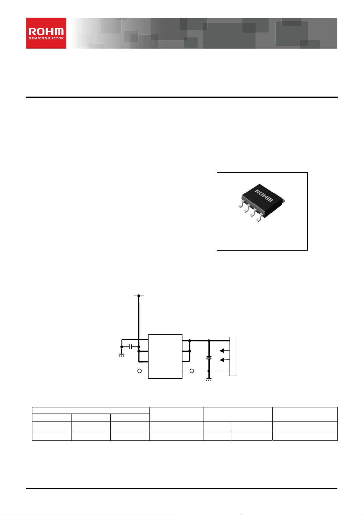
●Ty pical A pplication Circuit
C
IN
●Lineup
Over current detection
Min. Typ. Max.
0.7A 1.0A 1.6A Low SOP-J8 Reel of 2500 BD2041AFJ-E2
0.7A 1.0A 1.6A High SOP-J8 Reel of 2500 BD2051AFJ-E2
●Key Specifications
Input voltage range: 2.7V to 5.5V
Continuous current load: 0.5A(Typ.)
ON resistance : 80mΩ(Typ.)
Over current threshold: 0.7A min., 1.6A max.
Standby current: 0.01μA (Typ.)
Operating temperature range: -40℃ to +85℃
●Package W(Typ.) D(Typ.) H (Max.)
SOP-J8 4.90mm x 6.00mm x 1.65mm
5V(typ.)
GND
IN
IN
EN(/EN)
Control input logic Package Orderable Part Number
OUT
OUT
OUT
/OC
+
C
L
-
VBUS
D+
D-
GND
SOP-J8
○Product structure:Silicon monolithic integrated circuit ○This product is not designed protection against radioactive rays
www.rohm.com
© 2013 ROHM Co., Ltd. All rights reserved.
TSZ22111・14・001
1/22
TSZ02201-0E3E0H300290-1-2
08.Mar.2013 Rev.001
Datasheet
BD2041AFJ BD2051AFJ
/
●Block Diagram
GND
EN(/EN)
●Pin Configurations
1
GND
2
IN
IN
3
/EN
4
BD2041AFJ
TOP VIEW
●Pin Description
Pin No. Symbol I / O Pin function
1 GND I Ground.
2, 3 IN I
4 EN (/EN) I
5 /OC O
6, 7, 8 OUT O
IN
IN
Datasheet
OUT
UVLO
OUT
8
OUT
7
OUT
/OC
6
5
Charge
pump
Gate logic
TSD
OCD
1
2
3
4
Power supply input.
Input terminal to the power switch and power supply input terminal of the
internal circuit.
At use, connect each pin outside.
Enable input.
Power switch on at Low level. (BD2041AFJ)
Power switch on at High level. (BD2051AFJ)
High level input > 2.0V, Low level input < 0.8V.
Error flag output.
Low at over current, thermal shutdown.
Open drain output.
Power switch output.
At use, connect each pin outside.
OUT
OUT
/OC
BD2051AFJ
TOP VIEW
GND
IN
IN
EN
OUT
OUT
OUT
OC
8
7
6
5
www.rohm.com
© 2013 ROHM Co., Ltd. All rights reserved.
TSZ22111・15・001
2/22
TSZ02201-0E3E0H300290-1-2
08.Mar.2013 Rev.001

Datasheet
BD2041AFJ BD2051AFJ
●Absolute Maximum Ratings
Parameter Symbol Limits Unit
Supply voltage VIN -0.3 to 6.0 V
Enable voltage VEN, V/EN -0.3 to 6.0 V
/OC voltage V/OC -0.3 to 6.0 V
/OC current IS/OC 10 mA
OUT voltage VOUT -0.3 to 6.0 V
Storage temperature TSTG -55 to 150 °C
Power dissipation PD 560*1 mW
*1 In the case of exceeding Ta = 25°C, 4.48mW should be reduced per 1°C.
●Recommended Operating Ratings
Parameter Symbol Limits Unit
Operating voltage VIN 2.7 to 5.5 V
Operating temperature TOPR -40 to 85 °C
Continuous output current ILO 0 to 500 mA
●Electrical Characteristics
◎BD2041AFJ (Unless otherwise specified, V
Parameter Symbol
Operating Current IDD - 90 120 μA V/EN = 0V, OUT = OPEN
Standby Current ISTB - 0.01 1 μA V/EN = 5V, OUT = OPEN
V
/EN 2.0 - - V High input
/EN input voltage
/EN input current I/EN -1.0 .01 1.0 μA V/EN = 0V or V/EN = 5V
/OC output LOW voltage V/OC - - 0.5 V I/OC = 5mA
/OC output leak current IL/OC - 0.01 1 μA V/OC = 5V
ON resistance RON - 80 100 mΩ IOUT = 500mA
Over-current Threshold ITH 0.7 1.0 1.6 A
Output current at short ISC 0.7 1.0 1.3 A
Output rise time TON1 - 1.2 10 ms
Output turn on time TON2 - 1.5 20 ms
Output fall time TOFF1 - 1 20 μs
Output turn off time TOFF2 - 3 40 μs
UVLO threshold
V/EN
V
TUVH 2.1 2.3 2.5 V Increasing VIN
VTUVL 2.0 2.2 2.4 V Decreasing VIN
IN = 5.0V, Ta = 25°C)
Limits
Min. Typ. Max.
- - 0.8 V Low input
- - 0.4 V Low input 2.7V≤ VIN ≤4.5V
Unit Condition
VIN = 5V, VOUT = 0V,
C
L = 100μF (RMS)
RL = 10Ω, CL = OPEN
Datasheet
www.rohm.com
© 2013 ROHM Co., Ltd. All rights reserved.
TSZ22111・15・001
3/22
TSZ02201-0E3E0H300290-1-2
08.Mar.2013 Rev.001

Datasheet
BD2041AFJ BD2051AFJ
●Electrical Characteristics-Continued
◎BD2051AFJ (Unless otherwise specified, VIN = 5.0V, Ta = 25°C)
Parameter Symbol
Min. Typ. Max.
Limits
Unit Condition
Operating Current IDD - 90 120 μA VEN = 5V, OUT = OPEN
Standby Current I
EN input voltage
- 0.01 1 μA VEN = 0V, OUT = OPEN
STB
V
2.0 - - V High input
EN
VEN
- - 0.8 V Low input
- - 0.4 V Low input 2.7V≤ VIN ≤4.5V
EN input current IEN -1.0 0.01 1.0 μA VEN = 0V or VEN = 5V
/OC output LOW voltage V
/OC output leak current IL
- - 0.5 V I/OC = 5mA
/OC
- 0.01 1 μA V/OC = 5V
/OC
ON resistance RON - 80 100 mΩ IOUT = 500mA
IN = 5V, VOUT = 0V,
Output current at short ISC 0.7 1.0 1.3 A
Output rise time T
Output turn on time T
Output fall time T
Output turn off time T
- 1.2 10 ms
ON1
- 1.5 20 ms
ON2
- 1 20 μs
OFF1
- 3 40 μs
OFF2
V
L = 100μF (RMS)
C
L = 10Ω, CL = OPEN
R
Over-current Threshold ITH 0.7 1.0 1.6 A
V
2.1 2.3 2.5 V Increasing VIN
UVLO threshold
TUVH
V
2.0 2.2 2.4 V Decreasing VIN
TUVL
Datasheet
www.rohm.com
© 2013 ROHM Co., Ltd. All rights reserved.
TSZ22111・15・001
4/22
TSZ02201-0E3E0H300290-1-2
08.Mar.2013 Rev.001
Datasheet
BD2041AFJ BD2051AFJ
A
●Measurement Circuit
V
IN
Datasheet
V
IN
1uF
VEN(V
GND
IN
IN
EN(/EN)
)
/EN
OUT
OUT
OUT
/OC
A. Operating current B. EN, /EN input voltage, Output rise, fall time
V
IN
1uF
VEN(V
GND
IN
IN
EN(/EN)
)
/EN
OUT
OUT
OUT
/OC
C. ON resistance, Over current detection D. /OC output LOW voltage
●Timing Diagram
T
ON1
1uF
VEN(V
C
L
10k
V
IN
I
OUT
Figure 1. Measurement circuit
T
OFF1
/EN
1uF
)
VEN(V
GND
IN
IN
EN(/EN)
OUT
OUT
OUT
/OC
R
C
L
L
V
IN
GND
IN
IN
EN(/EN)
)
/EN
OUT
OUT
OUT
/OC
V
IN
I
/OC
T
OFF1
T
ON1
V
V
OUT
/EN
90%
10%
T
ON2
50% 50%
90%
10%
T
OFF2
V
OUT
V
EN
90%
10%
T
ON2
50% 50%
Figure 2. Timing diagram Figure 3. Timing diagram
BD2041AFJ BD2051AFJ
90%
10%
T
OFF2
www.rohm.com
© 2013 ROHM Co., Ltd. All rights reserved.
TSZ22111・15・001
5/22
TSZ02201-0E3E0H300290-1-2
08.Mar.2013 Rev.001

Datasheet
BD2041AFJ BD2051AFJ
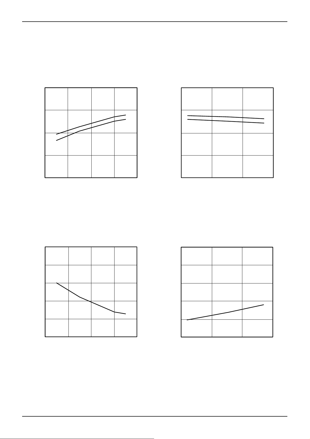
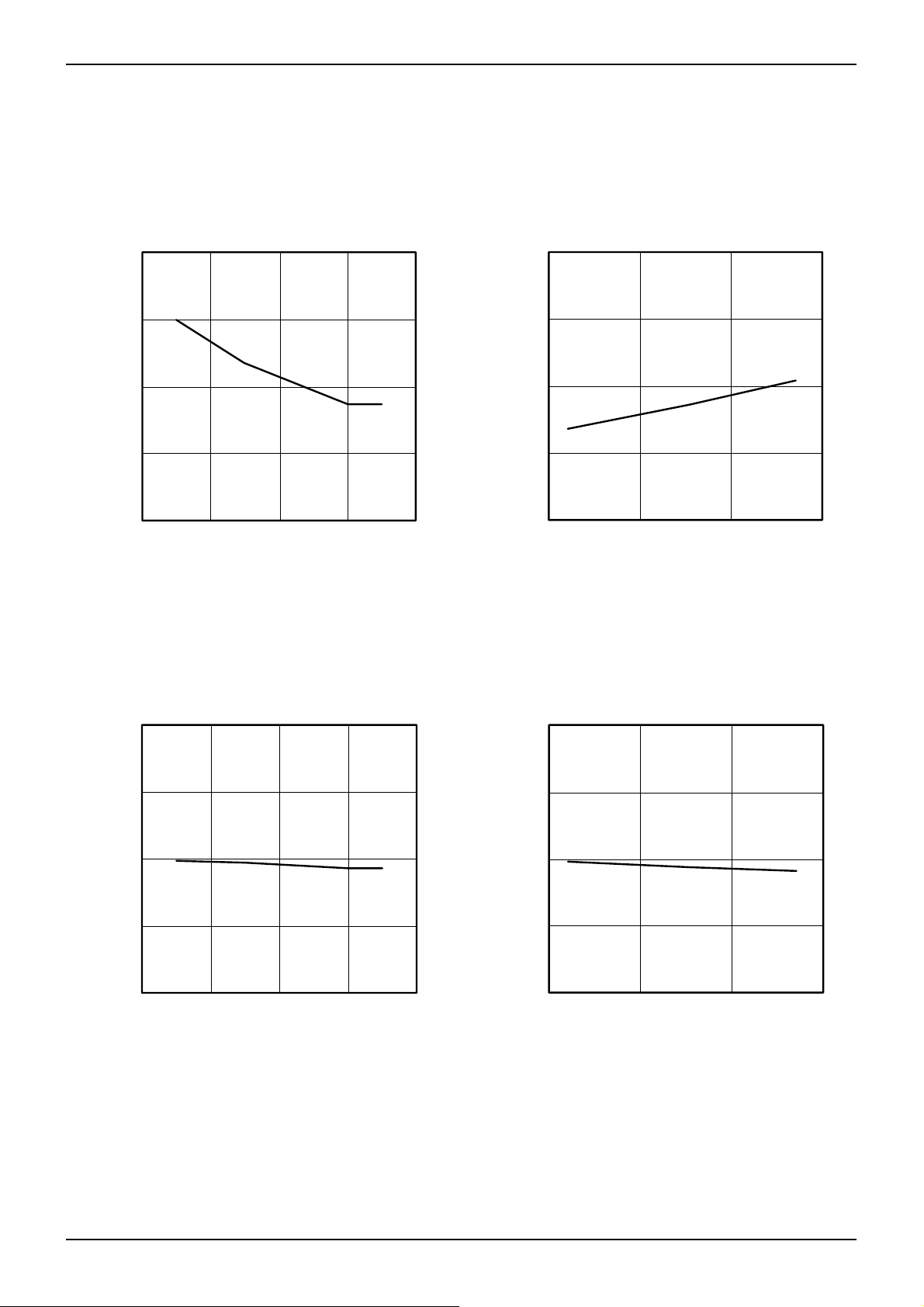
●Typical Performance Curves
Datasheet
120
Ta=25°C
100
80
[μA]
60
DD
I
40
OPERATING CURRENT :
20
0
23456
SUPPLY VOLTAGE : V
Figure 4. Operating current
EN,/EN Enable
[V]
IN
120
VIN=5.0V
100
80
[μA]
60
DD
I
40
OPERATING CURRENT :
20
0
-50 0 50 100
AMBIENT TEMPERATURE : Ta[℃]
Figure 5. Operating current
EN,/EN Enable
1.0
Ta=25°C
0.8
0.6
[μA]
STB
I
0.4
0.2
OPERATING CURRENT :
0.0
23456
SUPPLY VOLTAGE : V
Figure 6. Operating current
EN,/EN Disable
IN
[V]
1.0
VIN=5.0V
0.8
0.6
[μA]
STB
I
0.4
0.2
OPERATING CURRENT :
0.0
-50 0 50 100
AMBIENT TEMPERATURE : Ta[℃]
Figure 7. Operating current
EN,/EN Disable
www.rohm.com
© 2013 ROHM Co., Ltd. All rights reserved.
TSZ22111・15・001
6/22
TSZ02201-0E3E0H300290-1-2
08.Mar.2013 Rev.001
Datasheet
BD2041AFJ BD2051AFJ
w
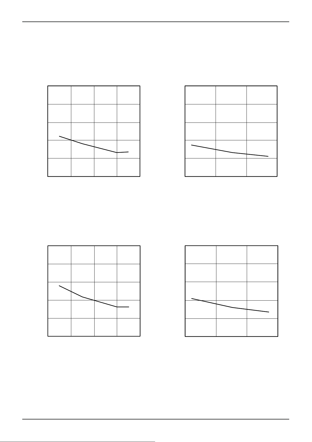
●Typical Performance Curves – Continued
Datasheet
2.0
Ta=25°C
1.5
Low to High
[V] 0
/EN
1.0
V
EN,
V
0.5
ENABLE INPUT VOLTAGE :
0.0
23456
SUPPLY VOLTAGE : V
Figure 8. EN,/EN input voltage
High to Low
[V]
IN
2.0
VIN=5.0V
1.5
[V]
/EN
1.0
, V
EN
V
Low to High
High to Lo
0.5
ENABLE INPUT VOLTAGE :
0.0
-50 0 50 100
AMBIENT TEMPERATURE : Ta[℃]
Figure 9. EN,/EN input voltage
0.5
Ta=25°C
0.4
0.3
[V]
/OC
V
0.2
0.1
/OC OUTPUT LOW VOLTAGE :
0.0
23456
SUPPLY VOLTAGE : V
Figure 10. /OC output LOW voltage
0.5
VIN=5.0V
0.4
0.3
[V]
/OC
V
0.2
0.1
/OC OUTPUT LOW VOLTAGE :
0.0
-50 0 50 100
[V]
IN
AMBIENT TEMPERATURE : Ta[℃]
Figure 11. /OC output LOW voltage
www.rohm.com
© 2013 ROHM Co., Ltd. All rights reserved.
TSZ22111・15・001
7/22
TSZ02201-0E3E0H300290-1-2
08.Mar.2013 Rev.001
Datasheet
BD2041AFJ BD2051AFJ
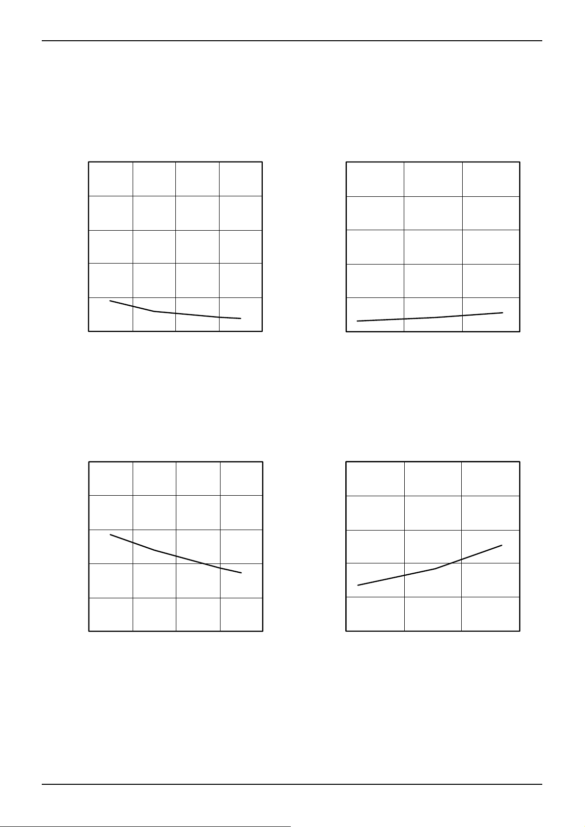
●Typical Performance Curves – Continued
Datasheet
ON RESISTANCE :
200
Ta=25°C
150
mΩ]
100
ON[
R
50
0
23456
SUPPLY VOLTAGE : V
Figure 12. ON resistance
[V]
IN
200
VIN=5.0V
150
[mΩ]
100
ON
R
ON RESISTANCE :
50
0
-50 0 50 100
AMBIENT TEMPERATURE : Ta[℃]
Figure 13. ON resistance
2.0
Ta=25°C
1.5
[A]
1.0
SC
I
0.5
SHORT CIRCUIT CURRENT :
0.0
23456
SUPPLY VOLTAGE : V
Figure 14. Output current at shortcircuit
(BD2041AFJ/51AFJ)
[V]
IN
2.0
VIN=5.0V
1.5
[A]
1.0
SC
I
0.5
SHORT CIRCUIT CURRENT :
0.0
-50 0 50 100
AMBIENT TEMPERATURE : Ta[℃]
Figure 15. Output current at shortcircuit
(BD2041AFJ/51AFJ)
www.rohm.com
© 2013 ROHM Co., Ltd. All rights reserved.
TSZ22111・15・001
8/22
TSZ02201-0E3E0H300290-1-2
08.Mar.2013 Rev.001
Datasheet
BD2041AFJ BD2051AFJ
●Typical Performance Curves – Continued
Datasheet
5.0
Ta=25°C
4.0
3.0
[ms]
ON1
2.0
T
RISE TIME :
1.0
0.0
23456
SUPPLY VOLTAGE : V
5.0
VIN=5.0V
4.0
3.0
[ms]
ON1
T
2.0
RISE TIME :
1.0
0.0
-50 0 50 100
[V]
IN
AMBIENT TEMPERATURE : Ta[℃]
Figure 17. Output rise time Figure 16. Output rise time
5.0
4.0
3.0
[ms]
ON2
T
2.0
TURN ON TIME :
1.0
0.0
Ta=25°C
23456
SUPPLY VOLTAGE : V
Figure 18. Output turn on time
[V]
IN
5.0
VIN=5.0V
4.0
3.0
[ms]
ON2
T
2.0
TURN ON TIME :
1.0
0.0
-50 0 50 100
AMBIENT TEMPERATURE : Ta[℃]
Figure 19. Output turn on time
www.rohm.com
© 2013 ROHM Co., Ltd. All rights reserved.
TSZ22111・15・001
9/22
TSZ02201-0E3E0H300290-1-2
08.Mar.2013 Rev.001
Datasheet
BD2041AFJ BD2051AFJ
●Typical Performance Curves – Continued
Datasheet
5.0
Ta=25°C
4.0
3.0
[μs]
OFF1
2.0
T
FALL TIME :
1.0
0.0
23456
SUPPLY VOLTAGE : V
Figure 20. Output fall time
5.0
VIN=5.0V
4.0
3.0
[µs]
OFF1
2.0
T
FALL TIME :
1.0
0.0
-50 0 50 100
[V]
IN
AMBIENT TEMPERATURE : Ta[℃]
Figure 21. Output fall time
5.0
Ta=25°C
4.0
3.0
[μs]
OFF2
T
2.0
TURN OFF TIME :
1.0
0.0
23456
SUPPLY VOLTAGE : V
Figure 22. Output turn off time
5.0
VIN=5.0V
4.0
3.0
[μs]
OFF2
OFF TIME :
2.0
T
TURN
1.0
0.0
-50 0 50 100
[V]
IN
AMBIENT TEMPERATURE : Ta[℃]
Figure 23. Output turn off time
www.rohm.com
© 2013 ROHM Co., Ltd. All rights reserved.
TSZ22111・15・001
10/22
TSZ02201-0E3E0H300290-1-2
08.Mar.2013 Rev.001

Datasheet
BD2041AFJ BD2051AFJ
UVLO HYSTERESIS VOLTAGE: VHYS
[V]
●Typical Performance Curves – Continued
Datasheet
2.5
2.4
V
UVLOH
[V]
2.3
UVLOL
, V
2.2
UVLOH
V
2.1
UVLO THRESHOLD VOLTAGE :
2.0
V
UVLOL
-50 0 50 100
AMBIENT TEMPERATURE : Ta[℃]
Figure 24. UVLO threshold voltage
1.0
0.8
0.6
0.4
0.2
0.0
-50 0 50 100
AMBIENT TEMPERA TURE: Ta[℃]
AMBIENT TEMP ERATURE : Ta [
℃
]
Figure 25. UVLO hysteresis voltage
www.rohm.com
© 2013 ROHM Co., Ltd. All rights reserved.
TSZ22111・15・001
11/22
TSZ02201-0E3E0H300290-1-2
08.Mar.2013 Rev.001

Datasheet
BD2041AFJ BD2051AFJ
●Typical Wave Forms
V
/EN
(5V/div.)
V
/OC
(5V/div.)
V
OUT
(5V/div.)
I
OUT
(0.5A/div.)
VIN=5V
RL=10Ω
CL=100μF
V
/EN
(5V/div.)
V
/OC
(5V/div.)
V
OUT
(5V/div.)
I
OUT
(0.5A/div.)
Datasheet
V
IN
R
L
=5V
=10Ω
=
V
/EN
(1V/div.)
I
OUT
(0.2A/div.)
V
/OC
(1V/div.)
TIME(1ms/div.)
Figure 26. Output rise characteristic
(BD2041AFJ)
220μF
47μF
TIME(0.5ms/div.)
330μF
V
R
=5V
IN
=10Ω
L
Figure 28. Inush current
(BD2041AFJ)
V
/OC
(5V/div.)
V
OUT
(5V/div.)
I
OUT
(0.5A/div.)
TIME(1ms/div.)
Figure 27. Output fall characteristic
(BD2041AFJ)
V
IN
TIME(20ms/div.)
Figure 29. Over current response
Ramped load
(BD2041AFJ)
=5V
www.rohm.com
© 2013 ROHM Co., Ltd. All rights reserved.
TSZ22111・15・001
12/22
TSZ02201-0E3E0H300290-1-2
08.Mar.2013 Rev.001

Datasheet
BD2041AFJ BD2051AFJ
(
)
(
●Typical Wave Forms – Continued
V
/OC
(5V/div.)
V
OUT
(5V/div.)
V
/EN
(5V/div.)
V
/OC
(5V/div.)
V
OUT
(5V/div.)
Datasheet
I
OUT
(0.5A/div.)
V
/OC
(5V/div.)
V
OUT
5V/div.)
V
=5V
IN
TIME(2ms/div.)
Figure 30. Over current response
Ramped load
(BD2041AFJ)
I
OUT
(0.5A/div.)
V
/OC
5V/div.
V
OUT
(5V/div.)
VIN=5V
C
TIME (2ms/div.)
Figure 31. Over current response
Enable to shortcircuit
(BD2041AFJ)
Thermal Shutdown
VIN=5V
C
L
=100μF
L
=100μF
I
I
OUT
(1A/div.)
OUT
(0.5A/div.)
VIN=5V
C
=100μF
L
TIME (2ms/div.)
Figure 32. Over current response
Figure 33. Over current response
Output shortcircuit at Enable
(BD2041AFJ)
www.rohm.com
© 2013 ROHM Co., Ltd. All rights reserved.
TSZ22111・15・001
13/22
TIME (500ms/div.)
Output shortcircuit at Enable
(BD2041AFJ)
TSZ02201-0E3E0H300290-1-2
08.Mar.2013 Rev.001

Datasheet
BD2041AFJ BD2051AFJ
(
(
(
)
(
)
●Typical Wave Forms – Continued
Datasheet
V
IN
(5V/div.)
V
OUT
5V/div.)
I
OUT
(0.5A/div.)
V
/OC
5V/div.)
TIME (10ms/div.)
Figure 34. UVLO
VDD increasing
(BD2041AFJ)
R
=10Ω
L
=
VIN
(5V/div.)
V
OUT
5V/div.
I
OUT
(0.5A/div.)
V
/OC
5V/div.
RL=10Ω
C
=147μF
L
TIME (10ms/div.)
Figure 35. UVLO
VDD decreasing
(BD2041AFJ)
Regarding the output rise/fall and over current detection characteristics of BD2051AFJ, refer to the characteri stic of BD2041AF J.
www.rohm.com
© 2013 ROHM Co., Ltd. All rights reserved.
TSZ22111・15・001
14/22
TSZ02201-0E3E0H300290-1-2
08.Mar.2013 Rev.001

Datasheet
BD2041AFJ BD2051AFJ
/OC
S
S
-D+GND
(
/EN)
●Ty pical A pplication Circuit
VBU
IN
Regulator
OUT
D
Datasheet
5V(typ.)
VBU
D+
D-
GND
USB
Controlle r
10kto
100kΩ
GND
CIN
IN
OUT
OUTIN
OUT
+
C
L
-
EN
●Application Information
When excessive current flows owing to output shortcircuit or so, ringing occurs by inductance of power source lin e to IC,
and may cause bad influences upon IC actions. In order to avoid this case, connect a bypath capacitor by IN terminal and
GND terminal of IC. 1μF or higher is recommended.
Pull up /OC output by resistance 10kΩ to 100kΩ.
Set up value which satisfies the application as C
This system connection diagram doesn’t guarantee operating as the application.
The external circuit constant and so on is changed and it uses, in which there are adequate margins by taking into account
external parts or dispersion of IC including not only static characteristics but also transient characteristics.
●Functional Description
1. Switch operation
IN terminal and OUT terminal are connected to the drain and the source of switch MOSFET respectively. And the IN
terminal is used also as power source input to internal control circuit.
When the switch is turned on from EN/EN control input, IN terminal and OUT terminal are connected by a 80mΩ switch.
In on status, the switch is bidirectional. Therefore, when the potential of OUT terminal is higher than that of IN terminal,
current flows from OUT terminal to IN terminal.
Since a parasitic diode between the drain and the source of switch MOSFET is canceled, in the off status, it is possible to
prevent current from flowing reversely from OUT to IN.
2. Thermal shutdown circuit (TSD)
If over current would continue, the temperature of the IC would increase drastically. If the junction temperature were
beyond 140°C (typ.) in the condition of over current detection, thermal shutdown circuit operates and makes power switch
turn off and outputs error flag (/OC). Then, when the junction temperature decreases lower than 120°C (typ.), power
switch is turned on and error flag (/OC) is cancelled. Unless the fact of the increasing chips temperature is removed or
the output of power switch is turned off, this operation repeats.
The thermal shutdown circuit operates when the switch is on (EN,/EN signal is active).
L.
www.rohm.com
© 2013 ROHM Co., Ltd. All rights reserved.
TSZ22111・15・001
15/22
TSZ02201-0E3E0H300290-1-2
08.Mar.2013 Rev.001

Datasheet
BD2041AFJ BD2051AFJ
3. Over current detection (OCD)
The over current detection circuit limits current (I
) and outputs error flag (/OC) when current flowing in each switch
SC
MOSFET exceeds a specified value. There are three types of response against over current. The over current detection
circuit works when the switch is on (EN,/EN signal is active).
3-1. When the switch is turned on while the output is in shortcircuit status
When the switch is turned on while the output is in shortcircuit status or so, the switch gets in current limit status
soon.
3-2. When the output shortcircuits while the switch is on
When the output shortcircuits or large capacity is connected while the switch is on, very large current flo ws until the
over current limit circuit reacts. When the current detection, limit circuit works, current limitation is carried out.
3-3. When the output current increases gradually
When the output current increases gradually, current limitation does not work until the output current exceeds the
over current detection value. When it exceeds the detection value, current limitation is carried out.
4. Under voltage lockout (UVLO)
UVLO circuit prevents the switch from turning on until the V
IN exceeds 2.3V(Typ.). If the VIN drops below 2.2V(Typ.) while
the switch turns on, then UVLO shuts off the power switch. UVLO has hysteresis of a 100mV(Typ).
Under voltage lockout circuit works when the switch is on (EN,/EN signal is active).
5. Error flag (/OC) output
Error flag output is N-MOS open drain output. At detection of over current, thermal shutdown, low level is output.
Over current detection has delay filter. This delay filter prevents instantaneous current detection such as inrush current at
switch on, hot plug from being informed to outside.
/EN
V
Datasheet
V
OUT
Output shortcircuit
Thermal shut down
OUT
I
/OC
V
delay
Figure 36. Over current detection, thermal shutdown timing
(BD2041AFJ)
VEN
V
OUT
Output shortcircuit
Thermal shut down
OUT
I
/OC
V
Figure 37. Over current detection, thermal shutdown timing
www.rohm.com
© 2013 ROHM Co., Ltd. All rights reserved.
TSZ22111・15・001
delay
(BD2051AFJ)
16/22
TSZ02201-0E3E0H300290-1-2
08.Mar.2013 Rev.001

Datasheet
BD2041AFJ BD2051AFJ
●Power Dissipation
(SOP-J8)
●I/O Equivalence Circuit
600
500
400
300
200
PO WER DISSIP A TION: Pd[mW ]
100
0
0 25 50 75 100 125 150
Symbol Pin No Equivalence circuit
Datasheet
A MBIENT T EMPERA T URE: Ta [℃]
Figure 38. Power dissipation curve (Pd-Ta Curve)
EN(/EN) 4
/OC 5
OUT 6,7,8
www.rohm.com
© 2013 ROHM Co., Ltd. All rights reserved.
TSZ22111・15・001
17/22
TSZ02201-0E3E0H300290-1-2
08.Mar.2013 Rev.001

Datasheet
BD2041AFJ BD2051AFJ
●Operational Notes
(1) Absolute Maximum Ratings
An excess in the absolute maximum ratings, such as supply voltage, temperature range of operating conditions, etc., can
break down devices, thus making impossible to identify breaking mode such as a short circuit or an open circuit. If any
special mode exceeding the absolute maximum ratings is assumed, consi derati on sh ould be g iven to take ph ys ical s afet y
measures including the use of fuses, etc.
(2) Operating conditions
These conditions represent a range within which characteristics can be provided approximately as expe c ted.
The electrical characteristics are guaranteed under the conditions of each parameter.
(3) Reverse connection of power supply connector
The reverse connection of power supply connector can break down ICs. Take protective measures against the
breakdown due to the reverse connection, such as mounting an external diode between the po wer supply and the IC’s
power supply terminal.
(4) Power supply line
Design PCB pattern to provide low impedance for the wiring between the power supply and the GND lines. In this regard,
for the digital block power supply and the analog block power supply, even though these power supplies has the same
level of potential, separate the power supply pattern for the digital block from that for the analog block, thus suppressing
the diffraction of digital noises to the analog block power supply resulting from impedanc e common to t he wiring patterns.
For the GND line, give consideration to design the patterns in a similar manner.
Furthermore, for all power supply terminals to ICs, mount a capacitor between the power supply and the GND terminal. At
the same time, in order to use an electrolytic capacitor, thoroughly check to be sure the characteristics of the capacitor to
be used present no problem including the occurrence of capacity dropout at a lo w temperature, thus determin ing the
constant.
(5) GND voltage
Make setting of the potential of the GND terminal so that it will be maintained at the mi nimum in any operating state.
Furthermore, check to be sure no terminals are at a potential lower than the GND voltage including an actual electric
transient.
(6) Short circuit between terminals and erroneous mounting
In order to mount ICs on a set PCB, pay thorough attention to the direction and offset of the ICs. Erroneous mounting can
break down the ICs. Furthermore, if a short circuit occurs due to foreign matters entering bet ween terminals or between
the terminal and the power supply or the GND terminal, the ICs can break down.
(7) Operation in strong electromagnetic field
Be noted that using ICs in the strong electromagnetic field can malfunction them.
(8) Inspection with set PCB
On the inspection with the set PCB, if a capacitor is connected to a low-impedance IC terminal, the IC can suffer stress.
Therefore, be sure to discharge from the set PCB by each process. Furthermore, in order to mount or dismount the set
PCB to/from the jig for the inspection process, be sure to turn OFF the power supply and then mount the set PCB to the
jig. After the completion of the inspection, be sure to turn OFF the power supply and then dismo unt it from the jig. In
addition, for protection against static electricity, establish a ground for the assembly process and pay thorough attention
to the transportation and the storage of the set PCB.
(9) Input terminals
In terms of the construction of IC, parasitic elements are inevitably formed in relation to potential. The operation of the
parasitic element can cause interference with circuit operation, thus resulting in a malfunction and then break down of the
input terminal. Therefore, pay thorough attention not to handle the input terminals, such as to apply to the input terminals
a voltage lower than the GND respectively, so that any parasitic element will operate. Furthermore, do not apply a vo ltage
to the input terminals when no power supply voltage is applied to the IC. In addition, even if the power supply voltage is
applied, apply to the input terminals a voltage lower than the power supply voltage or within the guarantee d value of
electrical characteristics.
Datasheet
www.rohm.com
© 2013 ROHM Co., Ltd. All rights reserved.
TSZ22111・15・001
18/22
TSZ02201-0E3E0H300290-1-2
08.Mar.2013 Rev.001

Datasheet
BD2041AFJ BD2051AFJ
(10) Ground wiring pattern
If small-signal GND and large-current GND are provided, It will be recommended to separate the large-current GND
pattern from the small-signal GND pattern and establish a single ground at the reference point of the set PCB so that
resistance to the wiring pattern and voltage fluctuations due to a large current will cause no fluctuations in voltages of the
small-signal GND. Pay attention not to cause fluctuations in the GND wiring pattern of external parts as well.
(11) External capacitor
In order to use a ceramic capacitor as the external capacitor, determine the constant with consideration given to a
degradation in the nominal capacitance due to DC bias and changes in the capacitance due to temperature, etc.
(12) Thermal shutdown circuit (TSD)
When junction temperatures become detected temperatures or higher, the thermal shutdown circuit operates and turns a
switch OFF. The thermal shutdown circuit is aimed at isolating the LSI from thermal runa way as much as possible. Do
not continuously use the LSI with this circuit operating or use the LSI assuming its operation.
(13) Thermal design
Perform thermal design in which there are adequate margins by taking into account the power dissipation (Pd) in actual
states of use.
Datasheet
www.rohm.com
© 2013 ROHM Co., Ltd. All rights reserved.
TSZ22111・15・001
19/22
TSZ02201-0E3E0H300290-1-2
08.Mar.2013 Rev.001

Datasheet
BD2041AFJ BD2051AFJ
●Ordering Information
B D 2 0 4 1 A F J - E 2
Part Number
Package
FJ: SOP-J8
Packaging and forming specification
E2: Embossed tape and reel
B D 2 0 5 1 A F J - E 2
Part Number
●Marking Diagram
SOP-J8 (TOP VIEW)
Part Number Part Number Marking
Part Number Marking
LOT Number
1PIN MARK
Package
FJ: SOP-J8
Packaging and forming specification
E2: Embossed tape and reel
Datasheet
BD2041AFJ D041A
BD2051AFJ D051A
www.rohm.com
© 2013 ROHM Co., Ltd. All rights reserved.
TSZ22111・15・001
20/22
TSZ02201-0E3E0H300290-1-2
08.Mar.2013 Rev.001

Datasheet
BD2041AFJ BD2051AFJ
●Physical Dimension, Tape and Reel Information
Package Name SOP-J8
Datasheet
<Tape and Reel information>
Quantity
Direction
of feed
www.rohm.com
© 2013 ROHM Co., Ltd. All rights reserved.
TSZ22111・15・001
Embossed carrier tapeTape
2500pcs
E2
The direction is the 1pin of product is at the upper left when you hold
()
reel on the left hand and you pull out the tape on the right hand
Direction of feed
TSZ02201-0E3E0H300290-1-2
08.Mar.2013 Rev.001
Reel
1pin
Order quantity needs to be multiple of the minimum quantity.
∗
21/22

Datasheet
BD2041AFJ BD2051AFJ
●Revision History
Date Revision Changes
08.Mar.2013 001 New Release
Datasheet
www.rohm.com
© 2013 ROHM Co., Ltd. All rights reserved.
TSZ22111・15・001
22/22
TSZ02201-0E3E0H300290-1-2
08.Mar.2013 Rev.001

Datasheet
Datasheet
Notice
●General Precaution
1) Before you use our Products, you are requested to carefully read this document and fully understand its contents.
ROHM shall not be in any way responsible or liable for failure, malfunction or accident arising from the use of a ny
ROHM’s Products against warning, caution or note contained in this document.
2) All information contained in this document is current as of the issuing date and subject to change without any prior
notice. Before purchasing or using ROHM’s Products, please confirm the latest information with a ROHM sales
representative.
●Precaution on using ROHM Products
1) Our Products are designed and manufactured for application in ordinary electronic equipments (such as AV equipment,
OA equipment, telecommunication equipment, home electronic appliances, amusement equipment, etc.). If you
intend to use our Products in devices requiring extremely high reliability (such as medical equipment, transport
equipment, traffic equipment, aircraft/spacecraft, nuclear power controllers, fuel controllers, car equipment including car
accessories, safety devices, etc.) and whose malfunction or failure may cause loss of human life, bodily injury or
serious damage to property (“Specific Applications”), please consult with the ROHM sales representative in advance.
Unless otherwise agreed in writing by ROHM in advance, ROHM shall not be in any way respons ible or liable for any
damages, expenses or losses incurred by you or third parties arising from the use of any ROHM’s Products for Specific
Applications.
2) ROHM designs and manufactures its Products subject to strict quality control system. However, semiconductor
products can fail or malfunction at a certain rate. Please be sure to implement, at your own responsibilities, adequate
safety measures including but not limited to fail-safe design against the physical injury, damage to any propert y, which
a failure or malfunction of our Products may cause. The following are examples of safety measures:
[a] Installation of protection circuits or other protective devices to improve system safety
[b] Installation of redundant circuits to reduce the impact of single or multiple circuit failure
3) Our Products are designed and manufactured for use under standard conditions and not under any special or
extraordinary environments or conditions, as exemplified below. Accordingly, ROHM shall not be in any way
responsible or liable for any damages, expenses or losses arising from the use of any ROHM’s Products under any
special or extraordinary environments or conditions. If you intend to use our Products under any special or
extraordinary environments or conditions (as exemplified below), your independent verification and confirmation of
product performance, reliability, etc, prior to use, must be necessary:
[a] Use of our Products in any types of liquid, including water, oils, chemicals, and organic solvents
[b] Use of our Products outdoors or in places where the Products are exposed to direct sunlight or dust
[c] Use of our Products in places where the Products are exposed to sea wind or corrosive gases, including Cl
H
2S, NH3, SO2, and NO2
[d] Use of our Products in places where the Products are exposed to static electricity or electromagnetic waves
[e] Use of our Products in proximity to heat-producing components, plastic cords, or other flammable items
[f] Sealing or coating our Products with resin or other coating materials
[g] Use of our Products without cleaning residue of flux (even if you use no-clean type fluxes, cleaning residue of
flux is recommended); or Washing our Products by using water or water-solub le cleaning agents for cleaning
residue after soldering
[h] Use of the Products in places subject to dew condensation
4) The Products are not subject to radiation-proof design.
5) Please verify and confirm characteristics of the final or mounted products in using the Products.
6) In particular, if a transient load (a large amount of load applied in a short per iod of time, such as pulse) is applied,
confirmation of performance characteristics after on-board mounting is strongly recomm ended. Avoid applying power
exceeding normal rated power; exceeding the power ratin g under steady-state loading condition may negatively affect
product performance and reliability.
7) De-rate Power Dissipation (Pd) depending on Ambient temperature (Ta). When used in se aled area, confirm the actual
ambient temperature.
8) Confirm that operation temperature is within the specified range described in the product specificati on.
9) ROHM shall not be in any way responsible or liable for failure induced under deviant co ndition from what is defined in
this document.
2,
Notice - Rev.004
© 2013 ROHM Co., Ltd. All rights reserved.

Datasheet
●Precaution for Mounting / Circuit board design
1) When a highly active halogenous (chlorine, bromine, etc.) flux is used, the residue of flux may negatively affect product
performance and reliability.
2) In principle, the reflow soldering method must be used; if flow soldering method is preferred, please consult with the
ROHM representative in advance.
For details, please refer to ROHM Mounting specification
●Precautions Regarding Application Examples and External Circuits
1) If change is made to the constant of an external circuit, please allow a sufficient margi n considering variations of the
characteristics of the Products and external components, including transient characteristics, as well as static
characteristics.
2) You agree that application notes, reference designs, and a ssociated data and information contained in this document
are presented only as guidance for Products use. Therefore, in case you use such information, you are solely
responsible for it and you must exercise your own independent verification and judgmen t in the use of such information
contained in this document. ROHM shall not be in any way responsible or liable for any damages, expenses or losses
incurred by you or third parties arising from the use of such information.
●Precaution for Electrostatic
This Product is electrostatic sensitive product, which may be damaged due to electrostatic discharge. Please take proper
caution in your manufacturing process and storage so that voltage exceeding the Products maximum rating will not be
applied to Products. Please take special care under dr y condition (e.g. Gro unding of human bod y / equipment / solder iron,
isolation from charged objects, setting of Ionizer, friction prevention and temperature / humidity control).
●Precaution for Storage / Transportation
1) Product performance and soldered connections may deteriorate if the Products are stored in the places where:
[a] the Products are expos ed to sea winds or corrosive gases, including Cl2, H2S, NH3, SO2, and NO2
[b] the temperature or humidity exceeds those recommended by ROHM
[c] the Products are exposed to direct sunshine or condensation
[d] the Products are expos ed to high Electrostatic
2) Even under ROHM recommended storage conditi on, solderabilit y of products out of recommended storage time period
may be degraded. It is strongly recommended to confirm solderabilit y before using Products of which storage time is
exceeding the recommended storage time period.
3) Store / transport cartons in the correct direct ion, which is indicated on a carton with a symbol. Otherwise bent leads
may occur due to excessive stress applied when dropping of a carton.
4) Use Products within the specified time after opening a humidity barrier bag. Baking is required before using Products of
which storage time is exceeding the recommended storage time period.
●Precaution for Product Label
QR code printed on ROHM Products label is for ROHM’s internal use only.
●Precaution for Disposition
When disposing Products please dispose them properly using an authorized industry waste company.
●Precaution for Foreign Exchange and Foreign Trade act
Since our Products might fall under controlled goods prescribed by the applicable foreign exchange and foreign trade act,
please consult with ROHM representative in case of export.
●Precaution Regarding Intellectual Property Rights
1) All information and data including but not limited to application example contained in this document is for reference
only. ROHM does not warrant that foregoing information or data will not infringe an y intellectual property rights or any
other rights of any third party regarding such information or data. ROHM shall not be in any way responsible or liable
for infringement of any intellectual property rights or other damages arising from use of such information or data.:
No license, expressly or implied, is granted hereby under any intellectual property rights or other rights of ROHM or any
2)
third parties with respect to the information contained in this document.
Datasheet
Notice - Rev.004
© 2013 ROHM Co., Ltd. All rights reserved.

Datasheet
●Other Precaution
1) The information contained in this document is provided on an “as is” basis and ROHM does not warrant that all
information contained in this document is accurate and/or error-free. ROHM shall not be in any way responsible or
liable for any damages, expenses or losses incurred by you or third parties resulting from inaccuracy or errors of or
concerning such information.
2) This document may not be reprinted or reproduced, in whole or in part, without prior written consent of ROHM.
3) T he Products may not be disassembled, converted, modified, reproduced or otherwise changed without prior written
consent of ROHM.
4) In no event shall you use in any way whatsoever the Products and the related technical informatio n contained in the
Products or this document for any military purposes, including but not limited to, the development of mass-destruction
weapons.
5) T he proper names of companies or products described in this document are trademarks or registered trademarks of
ROHM, its affiliated companies or third parties.
Datasheet
Notice - Rev.004
© 2013 ROHM Co., Ltd. All rights reserved.
 Loading...