

LED Drivers for LCD Backlights
Backlight LED Drivers
for Small LCD Panels (Charge Pump Type)
BD1604MUV, BD1604M VV
●Description
This LSI is a 4 white LED driver for small LCD backlight. At the charge pump type, the number of external devices is
minimized.
●Features
1) 4 parallel LED driver is mounted.
2) The LED current can be controlled via an external resistance.
3) Maximum current is 120mA (30mA × 4).
4) LED1 to LED4 can be turned on or off via an external control pin.
5) The relative current accuracy among LEDs (LED1 to LED4) is 3%.
6) Automatically transition to each mode (×1.0, ×1.5, ×2.0).
7) High efficiency (90% or more at maximum) is achieved.
8) Various protection functions such as output voltage protection function, current overload limiter and thermal shutdown
circuit are mounted.
●Applications
This driver provides for:
- Backlight using white LED
- Auxiliary lights for mobile phone cameras and simplified flash
●Lineup
Parameter BD1604MUV BD1604MVV
Number of LED channels 4ch 4ch
No.11040EBT23
Maximum current 120mA 120mA
Package
●Absolute Maximum Rating (Ta=25℃)
Parameter Symbol Ratings Unit
Power supply voltage Vmax 7 V
BD1604MUV
Allowable loss
BD1604MVV 780 *2
Operating temperature range Topr -30~85 ℃
Storage temperature range Tstr -55~150 ℃
*1 When a glass epoxy substrate (70mm×70mm×1.6mm) has been mounted, this loss will decrease 5.6mW/℃ if Ta is higher than or equal to 25℃.
*2 When a glass epoxy substrate (70mm×70mm×1.6mm) has been mounted, this loss will decrease 6.24mW/℃ if Ta is higher than or equal to 25℃.
●Recommended Operation Range
Parameter Symbol Limits Unit Condition
Operating supply voltage VBAT 2.7~5.5 V VBAT voltage
VQFN016V3030
3.00mm×3.00mm
Pd
SQFN016V4040
4.00mm×4.00mm
1
700 *
mW
www.rohm.com
© 2011 ROHM Co., Ltd. All rights reserved.
1/10
2011.06 - Rev.B
BD1604MUV, BD1604M VV
●Electrical Characteristics
Unless otherwise specified, Ta is 25℃ and VBAT is 3.6V.
Parameter Symbol
[Circuit current]
Circuit current 0 IQ0 - 0.1 1 μA EN=0V
Circuit current 1.0 IQ1.0 - 1.0 2.0 mA x1.0 Mode, Iout = 0mA
Circuit current 1.5 IQ1.5 - 2.3 3.3 mA x1.5 Mode, Iout = 0mA
Circuit current 2.0 IQ2.0 - 2.5 3.5 mA X2.0 Mode, Iout = 0mA
Unless otherwise specified, Ta is 25℃ and VBAT is 3.6V.
Parameter Symbol
[Current driver]
LED maximum current ILEDmax - - 30 mA
LED current accuracy ILEDdiff - 0.5 5.0 % ILED=10mA
Min. Typ. Max.
Min. Typ. Max.
Limits
Limits
Unit Condition
Unit Condition
Technical Note
LED current matching ILEDmatch - 0.5 3.0 % ILED=10mA *1)
LED pin control voltage VLED 0.08 0.10 0.20 V
ISET voltage ISET 0.5 0.6 0.7 V
Oscillation frequency Fosc 0.8 1.0 1.2 MHz
Over current limiter IOV - 600 900 mA
LED current limiter ILEDOV 40 60 100 mA
*1) LED current matching = (ILEDmax-ILEDmin)/(ILEDmax+ILEDmin)*100
ILEDmax : Maximum value of LED1-4 current
ILEDmin : Minimum value of LED1-4 current
Unless otherwise specified, Ta is 25℃ and VBAT is 5.5V.
Parameter Symbol
[Control Signal etc.]
Input ’H’ voltage VIH 1.4 - - V EN,SEL0,SEL1,SEL2
Input ’L’ voltage VIL - - 0.4 V EN,SEL0,SEL1,SEL2
Input ‘H’ current1 IIH1 - 18.3 30 μA EN=5.5V
Min. Typ. Max.
Limits
Unit Condition
Minimum voltage
at LED1~LED4 pins
Input ‘H’ current2 IIH2 - 0 1 μA SEL0,SEL1,SEL2=5.5V
Input ‘L’ current IIL -1 0 - μA EN,SEL0,SEL1,SEL2=0V
Unless otherwise specified, Ta is 25℃ and VBAT is 3.6V.
2/10
Limits
Unit Condition
2011.06 - Rev.B
Parameter Symbol
[Control Signal etc.]
UVLO detecting voltage VUVLO 1.9 2.2 2.5 V
www.rohm.com
© 2011 ROHM Co., Ltd. All rights reserved.
Min. Typ. Max.
BD1604MUV, BD1604M VV
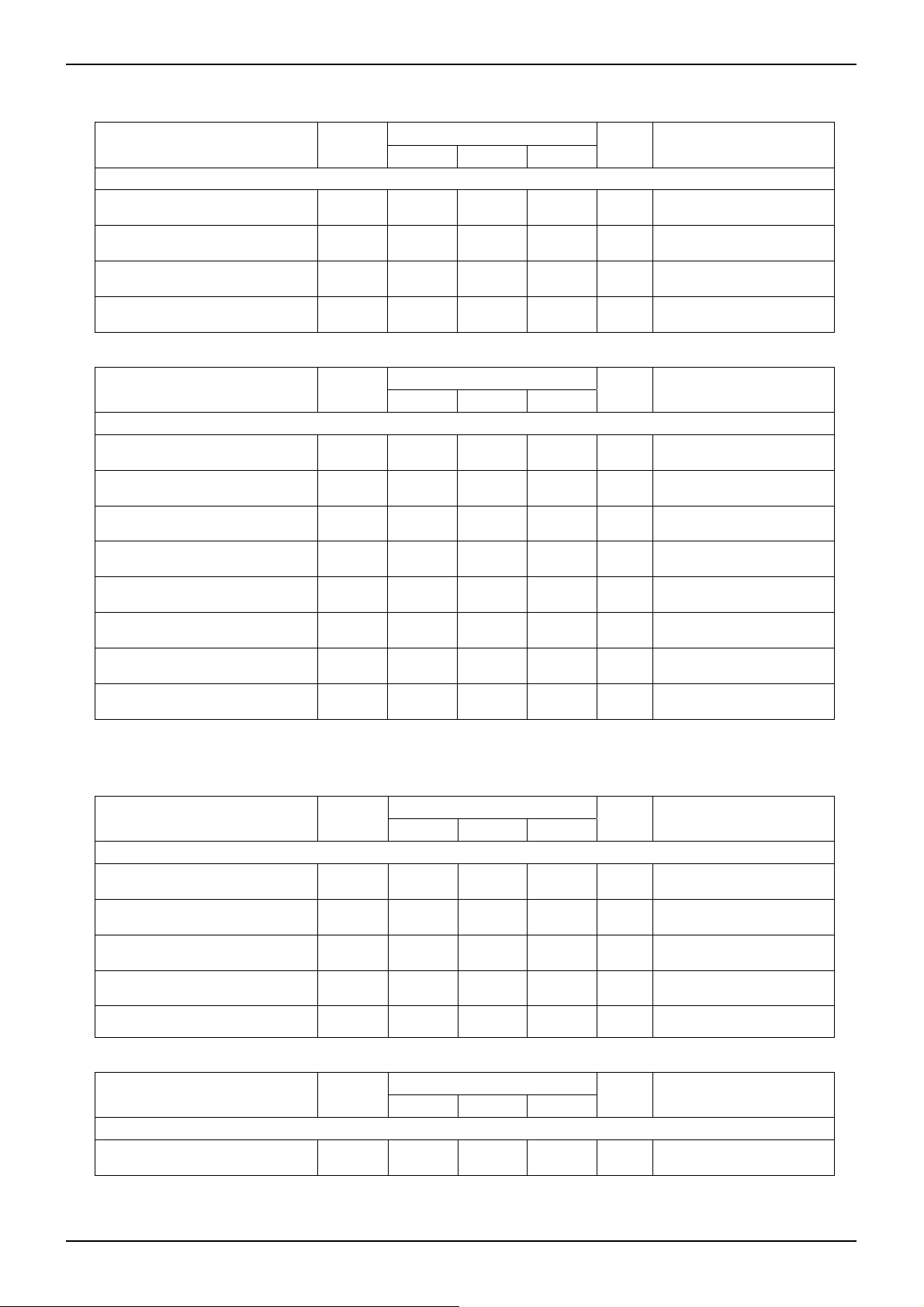
●Reference Data (Evaluation under LED VF=3.2V)
0.5
0.4
0.3
1.5
0.2
0.1
STAND-BY Current : Istb [µA]
0
3 3.5 4 4.5 5 5.5
INPUT VOLTAGE : VBAT[V]
Fig.1 Circuit Current
(Standby)
100
90
80
70
60
EFFICIENCY [%]
50
40
2.533.544.555.5
SUPPLY VOLTAGE : VBAT[V]
Fig.4 Efficiency
(5mA × 4 LEDs)
25
Ta=25
Ta=85℃
℃
20
15
10
5
LED CURRENT : ILE D [mA]
Ta=85℃
Ta=25
Ta=-30
Ta=85
Ta=25℃
Ta=-30
℃
Ta=-30
℃
℃
℃
℃
0.5
Current Consumption : IQ1.0 [µA]
100
90
80
70
60
EFFICIENCY [%]
50
40
25
20
15
10
LED CURRENT : ILE D [mA]
0
0 0.3 0.6 0.9 1.2
LED VOLTAGE : VLED[V]
Fig.7 LED Current (20mA)
(VBAT=2.7V)
35
30
25
20
15
ILED [mA]
10
5
0
0 50 100 150 200
RSET[kO]
Fig.10 LED Current vs. RSET
(Ta=25℃)
25
20
15
ILED [mA]
10
2
Ta=25
Ta=85℃
℃
Ta=-30
℃
1
0
012345
INPUT VOLTAGE : VBAT[V]
Fig.2 Circuit Current
(×1.0 Mode Operation)
Ta=-30
℃
℃
Ta=25
Ta=85℃
2.533.544.555.5
SUPPLY VOLTAGE : VBAT[V]
Fig.5 Efficiency
(15mA × 4 LEDs)
Ta=85℃
Ta=25
℃
5
0
0 0.3 0.6 0.9 1.2
LED VOLTAGE : VLED[V]
Ta=-30
℃
Fig.8 LED Current (20mA)
(VBAT=3.6V)
5
0
0 20406080100
PWM DUTY[%]
Fig.11 LED Current vs. PWM Duty
(Cycle 100Hz)
Technical Note
100
90
DOWN
80
70
60
EFFICIENCY [%]
50
40
2.533.544.5 55.5
Fig.3 Efficiency Hysteresis
100
90
Ta=-30
80
70
60
EFFICIENCY [%]
50
40
2.533.544.555.5
25
20
15
10
5
LED CURRENT : ILE D [mA]
0
0 0.3 0.6 0.9 1.2
Fig.9 LED Current (20mA)
UP
SUPPLY VOLTAGE : VBAT[V]
(20mA × 4 LEDs)
℃
℃
Ta=25
Ta=85℃
SUPPLY VOLTAGE : VBAT[V]
Fig.6 Efficiency
(20mA × 4 LEDs)
Ta=85℃
℃
Ta=25
LED VOLTAGE : VLED[V]
Ta=-30
℃
(VBAT=5.5V)
www.rohm.com
© 2011 ROHM Co., Ltd. All rights reserved.
3/10
2011.06 - Rev.B
BD1604MUV, BD1604M VV
●Block Diagram, Recommended Circuit Example and Pin Location Diagram
C2N
C2P
LED1
GND
12 11 10 9
13
Technical Note
C1N
8
C1P
LED2
14
BD1604MUV
7
VBAT
BD1604MVV
6
5
VOUT
ISET
VOUT
Cout
Cin
Battery
VBAT
LED3
15
LED4
16
Charge Pump
Mode Control
1
2 3 4
EN
SEL0
SEL1
Fig.12 Pin Location Diagram
(Top View)
C1
C1N
C2
C2N
C1P
C2P
×1, ×1.5, ×2
Charge pump
Over Voltage
Protect
SEL2
EN
SEL0
SEL1
SEL2
ISET
Rset
Fig.13 Block Diagram and Recommended Circuit Diagram
www.rohm.com
© 2011 ROHM Co., Ltd. All rights reserved.
Control
ISET
Resistor Driver
GND
OSC
TSD
4/10
Vout Control
LED1
LED2
LED3
LED4
Current Driver
2011.06 - Rev.B

BD1604MUV, BD1604M VV
[Pin table]
Pin number
Pin name
BD1604MUV BD1604MVV
EN 1 1 F
SEL0 2 2 E
SEL1 3 3 E
SEL2 4 4 E
ISET 5 5 G
VOUT 6 6 C
VBAT 7 7 H
C1P 8 8 B
C1N 9 9 A
C2N 10 10 A
C2P 11 11 B
GND 12 12 I
LED1 13 13 D
LED2 14 14 D
LED3 15 15 D
LED4 16 16 D
●I/O Equivalence Circuit Diagram
The following shows I/O equivalence circuits.
A B C D
PAD
E F G H
PAD PAD PA D PAD
I
PAD
Technical Note
Pin circuit
diagram
PAD PADPAD
Fig.14 Pin Diagram
www.rohm.com
© 2011 ROHM Co., Ltd. All rights reserved.
5/10
2011.06 - Rev.B

BD1604MUV, BD1604M VV
●Description of Block Operations
1) LED light control and current control
When LED lights are controlled, H- or L-level voltage is applied to respective control pins.
Current control in the BD1604MUV/MVV can take place via a resistance connected to the ISET pin.
ON/OFF control
SEL2 SEL1 SEL0 LED1 LED2 LED3 LED4
0 0 0 OFF OFF OFF ON
0 0 1 OFF OFF ON OFF
0 1 0 OFF ON OFF OFF
0 1 1 ON OFF OFF OFF
1 0 0 OFF OFF ON ON
1 0 1 OFF ON ON ON
1 1 0 ON ON ON ON
1 1 1 OFF OFF OFF OFF
Rset: See the following table. 0: 0V, 1: VBAT
When handling pins, the LED pins must be connected to VBAT so long as LED is always OFF.
Current control
Rset 165kΩ 97.6kΩ 48.7kΩ 32.4kΩ 24.3kΩ 16.2kΩ
ILED 3mA 5mA 10mA 15mA 20mA 30mA
The LED current can be changed by the Rset value.
ILED=480/Rset
The above expression can be used for approximation.
2) Low supply voltage detection circuit (UVLO)
When the IC-applied supply voltage drops, all the circuits including the DC/DC converter are stopped. When supply voltage
drops to a detecting voltage, UVLO is activated. When it rises, UVLO is automatically released.
3) Soft start by DC/DC converter startup
When a DC/DC converter is started, soft start is enabled so that output voltage can be increased gradually to prevent output
voltage overshooting.
●Application Parts Selection Method
Capacitor (Use the ceramics parts with good frequency and temperature characteristics.)
Symbol Recommended value Recommended part Type
Cout,Cin,C1,C2 1μF GRM188B11A105KA61B(MURATA) Ceramics capacitor
Resistance
Symbol Recommended value Recommended part Set Current Value
16kΩ
Rset
~
MCR006YZPF Series (ROHM)
Technical Note
30mA
~
240kΩ 2mA
Connect an input bypass capacitor (CIN) between VBAT and GND pin in proximity. In addition, connect an output capacitor
between VOUT and GND pins in proximity. Connect a capacitor between C1P and C1N and also a capacitor between C2P
and C2N in proximity to the chips. Connect a resistance in proximity to the ISET pin.
When other than these parts are used, the equivalent parts must be used.
www.rohm.com
© 2011 ROHM Co., Ltd. All rights reserved.
6/10
2011.06 - Rev.B

BD1604MUV, BD1604M VV
Technical Note
●Cautions on layout pattern
When designing a layout pattern, lay out wires to a power line in a way that the layout pattern impedance can be minimized
and connect a bypass capacitor if necessary.
LED
VOUT
RSET
1μF
LED
GND
VBAT
1μF
1μF
1μF
GND
Wiring from the VBAT pin
to Cin must meet a low
impedance.
The GND pin and
Cin must be
placed nearby.
Fig.15 Example of BD1604MUV Layout Pattern Fig.16 Exam ple of BD1604MUV Layout Pattern
(Front, Top View) (Rear, Top View)
●LED Current Control
There are two methods for LED current control. One method uses an external PWM signal and another changes the
resistance value of RREF (RSET) connected to the IREF (ISET) pin. For details, refer to the respective circuit examples.
Don’t make the setting of 30mA or more per channel for BD1604MUV/MVV.
1) Controlling the current by using the PWM method
The PWN signal must be input to the EN pin.
PWM signal “H” level: 1.4V or more
PWM signal “L” level: 0.4V or less
When PWM Duty is used in an area of 10% or less, the PWM cycle must be a range from 100Hz to 200Hz. When extremely
high-speed PWM control takes place, the linearity of LED current value to PWM duty is lost if the PWM duty is small (for
example, 10% or less) or it is large (for example, 90% or more).
2) Controlling the current by changing the SET resistance value
Rset-Rset1=Rset2// … //Restn.
This means that the current can be adjusted more finely by adding the types of resistance values.
ILED=480/Rset [A]
The approximate LED current can be obta ined from the above expression. Because the current of 30mA or more per LED is not
permitted, make the setting in a way that the Rset resistance value can be maintained to be greater than or equal to16kΩ.
C2
Control
C1
C2N
C1N
C1P
×1, ×1.5, ×2
Charge pump
Over Voltage
Protect
OSC
TSD
C2P
PWM signal input (ON
for the signal set to High)
Cin
Battery
VBAT
SEL0
SEL1
SEL2
EN
Char ge P ump
Mode Control
ISET
Rset
ISET
Resistor Driver
GND
Current Driver
LED
LED
Vout Control
VOUT
Cout
LED1
LED2
LED3
LED4
C2
C1
C2N
C1N
C1P
Battery
VBAT
Cin
Char ge P ump
Mode C ontrol
EN
SEL0
SEL1
SEL2
ISET
Rset2Rsetn
Rset1
Resistor Driver
Control
ISET
GND
×1, ×1.5, ×2
Charge pump
Over Voltage
Protect
C2P
OSC
Vout Control
TSD
Current Driver
VOUT
Cout
LED1
LED2
LED3
LED4
Fig.17 Controlling the Current
by Using the PWM Method
www.rohm.com
© 2011 ROHM Co., Ltd. All rights reserved.
7/10
Fig.18 Controlling the Current
by Changing the Resistance Value
2011.06 - Rev.B

BD1604MUV, BD1604M VV
●Notes for Use
(1) Absolute Maximum Ratings
An excess in the absolute maximum ratings, such as supply voltage, temperature range of operating conditions, etc.,
can break down devices, thus making impossible to identify breaking mode such as a short circuit or an open circuit. If
any special mode exceeding the absolute maximum ratings is assumed, consideration should be given to take physical
safety measures including the use of fuses, etc.
(2) Operating conditions
These conditions represent a range within which characteristics can be provided a pproximately as expected. The
electrical characteristics are guaranteed under the conditions of each parameter.
(3) Reverse connection of power supply connector
The reverse connection of power supply connector can break down ICs. Take protective measures against the
breakdown due to the reverse connection, such as mounting an external diode between the power supply and the IC’s
power supply terminal.
(4) Power supply line
Design PCB pattern to provide low impedance for the wiring between the power supply and the GND lines. In this regard,
for the digital block power supply and the analog block power supply, even though these power supplies has the same
level of potential, separate the power supply pattern for the digital block from that for the analog block, thus suppressing
the diffraction of digital noises to the analog block power supply resulting from impedance common to the wiring patterns.
For the GND line, give consideration to design the patterns in a similar manner.
Furthermore, for all power supply terminals to ICs, mount a capacitor between the power supply and the GND terminal.
At the same time, in order to use an electrolytic capacitor, thoroughly check to be sure the characteristics of the
capacitor to be used present no problem including the occurrence of capacity dropout at a low temperature, thus
determining the constant.
(5) GND voltage
Make setting of the potential of the GND terminal so that it will be maintained at the minimum in any operating state.
Furthermore, check to be sure no terminals are at a potential lower than the GND voltage including an actual electric
transient.
(6) Short circuit between terminals and erroneous mounting
In order to mount ICs on a set PCB, pay thorough attention to the direction and offset of the ICs. Erroneous mounting
can break down the ICs. Furthermore, if a short circuit occurs due to foreign matters entering between terminals or
between the terminal and the power supply or the GND terminal, the ICs can break down.
(7) Operation in strong electromagnetic field
Be noted that using ICs in the strong electromagnetic field can malfunction them.
(8) Inspection with set PCB
On the inspection with the set PCB, if a capacitor is connected to a low-impedance IC terminal, the IC can suffer stress.
Therefore, be sure to discharge from the set PCB by each process. Furthermore, in order to mount or dismount the set
PCB to/from the jig for the inspection process, be sure to turn OFF the power supply and then mount the set PCB to the
jig. After the completion of the inspection, be sure to turn OFF the power supply and then dismount it from the jig. In
addition, for protection against static electricity, establish a ground for the assembly process and pay thorough attention
to the transportation and the storage of the set PCB.
(9) Input terminals
In terms of the construction of IC, parasitic elements are inevitably formed in relation to potential. The operation of the
parasitic element can cause interference with circuit operation, thus resulting in a malfunction and then breakdown of
the input terminal. Therefore, pay thorough attention not to handle the input terminals, such as to apply to the input
terminals a voltage lower than the GND respectively, so that any parasitic element will operate. Furthermore, do not
apply a voltage to the input terminals when no power supply voltage is applied to the IC. In addition, even if the power
supply voltage is applied, apply to the input terminals a voltage lower than the power supply voltage or within the
guaranteed value of electrical characteristics.
(10) Ground wiring pattern
If small-signal GND and large-current GND are provided, It will be recommended to separate the large-current GND
pattern from the small-signal GND pattern and establish a single ground at the reference point of the set PCB so that
resistance to the wiring pattern and voltage fluctuations due to a larg
the small-signal GND. Pay attention not to cause fluctuations in the GND wiring pattern of external parts as well.
Technical Note
e curre
nt will cause no fluctuations in voltages of
www.rohm.com
© 2011 ROHM Co., Ltd. All rights reserved.
8/10
2011.06 - Rev.B

BD1604MUV, BD1604M VV
(11) External capacitor
In order to use a ceramic capacitor as the external capacitor, determine the constant with consideration given to a
degradation in the nominal capacitance due to DC bias and changes in the capacitance due to temperature, etc.
(12) Not connecting input terminals
In terms of extremely high impedance of CMOS gate, to open the input terminals causes unstable state. Unstable state
occurs from the inside gate voltage of p-channel or n-channel transistor into active. As a result, power supply current
may increase. And unstable state can also cause unexpected operation of IC. So unless otherwise specified, input
terminals not being used should be connected to the power supply or GND line.
(13) Thermal shutdown circuit (TSD)
When junction temperatures become setting temperature or higher, the thermal shutdown circuit operates and turns a
switch OFF. The thermal shutdown circuit, which is aimed at isolating the LSI from thermal runaway as much as
possible, is not aimed at the protection or guarantee of the LSI. Therefore, do not continuously use the LSI with this
circuit operating or use the LSI assuming its operation.
(14) Thermal design
Perform thermal design in which there are adequate margins by taking into account the permissible diss ipation (Pd) in
actual states of use.
●Thermal Loss
The following conditions must be met for thermal design. (Because the following temperature is only the assured
temperature, be sure to consider the margin for design.)
1. The ambient temperature Ta must be 85˚C.
2. The IC loss must be smaller than an allowable loss (Pd).
●Power dissipation character
The following shows the power dissipation character.
1
0.78W
0.8
0.6
0.4
1
0.8
0.70W
0.6
0.4
POWER DISSIPATION : Pd[W]
POWER DISSIPATION : Pd[W]
0.2
0.2
0
0 25 50 75 100 125 150
TEMPARATURE[℃]
Fig.19 BD1604MVV
0
0 25 50 75 100 125 150
TEMPARATURE[℃]
Fig.20 BD1604MUV
Mount board specification
Material : Glass epoxy
Size : 70mm × 70mm × 1.6mm
Technical Note
www.rohm.com
© 2011 ROHM Co., Ltd. All rights reserved.
9/10
2011.06 - Rev.B

BD1604MUV, BD1604M VV
●Ordering part number
B D 1 6 0 4 M U V - E 2
Technical Note
Part No.
BD
VQFN016V3030
SQFN016V4040
Part No.
1604
3.0±0.1
3.0±0.1
0.4±0.1
1.0MAX
0.08 S
0.75
0.55±0.1
C0.2
1.0MAX
0.08 S
C0.2
1.025
16
13
16
13
1PIN MARK
1.4±0.1
1
12 9
4.0±0.1
1PIN MARK
2.1±0.1
1
12 9
0.5
4
5
8
+0.05
0.25
−0.04
4.0±0.1
0.65
4
5
8
+0.05
0.3
−0.04
+0.03
0.02
+0.03
−0.02
0.02
2.1±0.1
−0.02
1.4±0.1
S
(0.22)
(Unit : mm)
S
(0.22)
(Unit : mm)
Package
MUV: VQFN016V3030
MVV: SQFN016V4040
<Tape and Reel information>
Embossed carrier tapeTape
Quantity
Direction
of feed
<Tape and Reel information>
Quantity
Direction
of feed
3000pcs
E2
The direction is the 1pin of product is at the upper left when you hold
()
reel on the left hand and you pull out the tape on the right hand
Reel
Embossed carrier tapeTape
2500pcs
E2
The direction is the 1pin of product is at the upper left when you hold
()
reel on the left hand and you pull out the tape on the right hand
Reel
Packaging and forming specification
E2: Embossed tape and reel
1pin
Order quantity needs to be multiple of the minimum quantity.
∗
1pin
Order quantity needs to be multiple of the minimum quantity.
∗
Direction of feed
Direction of feed
www.rohm.com
© 2011 ROHM Co., Ltd. All rights reserved.
10/10
2011.06 - Rev.B

Notes
No copying or reproduction of this document, in part or in whole, is permitted without the
consent of ROHM Co.,Ltd.
The content specied herein is subject to change for improvement without notice.
The content specied herein is for the purpose of introducing ROHM's products (hereinafter
"Products"). If you wish to use any such Product, please be sure to refer to the specications,
which can be obtained from ROHM upon request.
Examples of application circuits, circuit constants and any other information contained herein
illustrate the standard usage and operations of the Products. The peripheral conditions must
be taken into account when designing circuits for mass production.
Great care was taken in ensuring the accuracy of the information specied in this document.
However, should you incur any damage arising from any inaccuracy or misprint of such
information, ROHM shall bear no responsibility for such damage.
The technical information specied herein is intended only to show the typical functions of and
examples of application circuits for the Products. ROHM does not grant you, explicitly or
implicitly, any license to use or exercise intellectual property or other rights held by ROHM and
other parties. ROHM shall bear no responsibility whatsoever for any dispute arising from the
use of such technical information.
The Products specied in this document are intended to be used with general-use electronic
equipment or devices (such as audio visual equipment, ofce-automation equipment, communication devices, electronic appliances and amusement devices).
The Products specied in this document are not designed to be radiation tolerant.
While ROHM always makes efforts to enhance the quality and reliability of its Products, a
Product may fail or malfunction for a variety of reasons.
Please be sure to implement in your equipment using the Products safety measures to guard
against the possibility of physical injury, re or any other damage caused in the event of the
failure of any Product, such as derating, redundancy, re control and fail-safe designs. ROHM
shall bear no responsibility whatsoever for your use of any Product outside of the prescribed
scope or not in accordance with the instruction manual.
The Products are not designed or manufactured to be used with any equipment, device or
system which requires an extremely high level of reliability the failure or malfunction of which
may result in a direct threat to human life or create a risk of human injur y (such as a medical
instrument, transportation equipment, aerospace machiner y, nuclear-reactor controller, fuelcontroller or other safety device). ROHM shall bear no responsibility in any way for use of any
of the Products for the above special purposes. If a Product is intended to be used for any
such special purpose, please contact a ROHM sales representative before purchasing.
If you intend to export or ship overseas any Product or technology specied herein that may
be controlled under the Foreign Exchange and the Foreign Trade Law, you will be required to
obtain a license or permit under the Law.
Notice
www.rohm.com
© 2011 ROHM Co., Ltd. All rights reserved.
Thank you for your accessing to ROHM product informations.
More detail product informations and catalogs are available, please contact us.
ROHM Customer Support System
http://www.rohm.com/contact/
R1120
A
 Loading...