

A
System Motor Driver ICs for CD/DVD Players
1ch Spindle
Motor Driver ICs
BA6859AFP-Y,BA6664FM,BD6671FM
●Description
ROHM’s spindle motor drivers incorporate the 3-phase full-wave pseudo-linear drive system(BA6859AFP-Y, BA6664FM)
and 180 ° electrifying direct PWM drive system(BD6671FM).Smooth rotation characteristic performance is ensured.
Besides, high torque is provided in a wide output range because the output stage incorporates low-saturation voltage NPN
transistors (BA6859AFP-Y, BA6664FM) and low-power consumption MOSFET (BA6671FM).
●Features
1) 3-phase full-wave pseudo-linear system (BA6859AFP-Y, BA6664FM)
2) 180° electrifying direct drive PWM system (BD6671FM)
3) Power saving, TSD (thermal shutdown) functions built in
4) Current limiting, Hall bias circuit built in
5) FG output built in
6) 3-phase component FG output built in (BA6664FM, BD6671FM)
7) Circuit direction detection function built in (BA6859AFP-Y, BA6664FM)
8) Reverse rotation prevention circuit built in
9) Short brake pin built in (BA6859AFP-Y, BA6664FM)
10) Brake mode selection pin built in (BA6859AFP-Y, BD6671FM)
11) Supports DSP 3.3 V
●Applications
Used for car, CD and DVD players incorporating changer function
●Absolute maximum ratings (Ta=25℃)
Parameter Symbol
Applied voltage VCC 7 7 7 V
Applied voltage VM 15 15 15 V
Applied voltage VG - - 20 V
Power dissipation Pd 1450*1 2200*2 2200*2 mW
Operating temperature Topr -40~+85 -40~+85 -40~+85 ℃
Storage temperature Tstg -55~+150 -55~+150 -55~+150 ℃
Output current Iout 1300 1300 2500 mA
Junction temperature Tjmax 150 150 150 ℃
*1 Reduced by 11.6 mW/℃ over 25℃, when mounted on a glass epoxy board (70 mm x 70 mm x 1.6 mm).
*2 Reduced by 17.6 mW/℃ over 25℃, when mounted on a glass epoxy board (70 mm x 70 mm x 1.6 mm).
●Line up matrix
Parameter Symbol
Power supply voltage
VG pin voltage VG - - 8.5~19 V
VCC 4.5~5.5 4.5~5.5 4.5~5.5 V
VM 3.0~14 3.0~14 4.0~13.2 V
BA6859AFP-Y BA6664FM BD6671FM
BA6859AFP-Y BA6664FM BD6671FM
Ratings
Ratings
No.10011EAT03
Unit
Unit
www.rohm.com
© 2010 ROHM Co., Ltd. All rights reserved.
1/17
2010.06 - Rev.
BA6859AFP-Y,BA6664FM,BD6671FM
A
●Electrical characteristics
1) BA6859AFP-Y (Unless otherwise specified, Ta=25℃, VCC=5.0V, VM=12V)
Parameter Symbol
Min. Typ. Max.
Limits
Unit Conditions
<Total device>
Circuit current 1 I
Circuit current 2 I
- 0 0.2 mA PS=L
CC1
- 5.0 7.5 mA PS=H
CC2
<Power-saving >
ON voltage range V
OFF voltage range V
- - 1.0 V Internal circuit OFF
PSON
2.5 - - V Internal circuit ON
PSOFF
<Hall bias>
Hall bias voltage VHB 0.5 0.9 1.5 V IHB=10mA
<Hall amp>
Input bias current IHA - 0.7 3.0 µA
Same phase input voltage range V
Mini. input level V
H3 hysteresis level V
1.0 - 4.0 V
HAR
50 - - mVpp One side input level
INH
5 20 40 mV
HYS
<Torque Command >
Input voltage range EC, E
Offset voltage - E
Offset voltage + E
Input bias current E
COFF-
COFF+
CIN
CR
-3 - 3 µA EC=ECR
0 - 5 V Linear range:0.5~3.3V
-80 -50 -20 mV ECR=1.9V
20 50 80 mV ECR=1.9V
I/O gain GEC 0.56 0.70 0.84 A/V EC=1.2, 1.7V
<FG>
FG output high-level voltage V
FG output low-level voltage V
4.5 4.8 - V IFG=-20µA
FGH
- 0.25 0.4 V IFG=3.0mA
FGL
Duty (reference values) DU - 50 - %
<Rotation Detection>
FR output high-level voltage V
FR output low-level voltage V
4.1 4.4 - V IFR=-20µA
FRH
- 0.25 0.4 V IFR=3.0mA
FRL
<Output>
Output saturation high level voltage VOH - 1.0 1.4 V IO=-600mA
Output saturation low level voltage VOL - 0.4 0.7 V IO=600mA
Pre-drive current I
- 35 70 mA EC=0V output open
VML
Output limit current ITL 560 700 840 mA
<Short brake >
ON voltage range V
OFF voltage range V
2.5 - - V BR=0V
SBON
- - 1.0 V BR=0V
SBOFF
<Brake mode >
ON voltage range V
OFF voltage range V
2.5 - - V EC>ECR, SB=Open
BRON
- - 1.0 V EC>ECR, SB=Open
BROFF
●Reference: Data
10
8
25℃
-40℃
85℃
6
4
2
Circui t curr ent :Icc2 [mA]
0
4.5 5 5.5 6 6.5 7
Supply voltag e :Vcc[v]
1.5
[V]
OH
1.0
0.5
Output H voltage:V
0.0
0 0.3 0.6 0.9 1.2 1.5
Output C urrent :IOH [v]
85℃
-40℃
25℃
Fig.1 Circuit Current 2
Fig.2 Output Saturation Voltage
at High Level
Fig.3 Output Saturation Voltage
Technical Note
1.5
[V]
OL
1.0
0.5
Output L voltage :V
0.0
0 0.3 0.6 0.9 1.2 1.5
Output C urrent :I
at Low Level
85℃
-40℃
OL
25℃
[A]
www.rohm.com
© 2010 ROHM Co., Ltd. All rights reserved.
2/17
2010.06 - Rev.

BA6859AFP-Y,BA6664FM,BD6671FM
A
2) BA6664FM(Unless otherwise specified, Ta=25℃, VCC=5.0V, VM=12V)
Parameter Symbol
Min. Typ. Max.
Limits
Unit Conditions
<Total device>
Circuit current 1 I
Circuit current 2 I
- 0 0.2 mA PS=L, GSW=Open
CC1
- 6.2 9.1 mA PS=H, GSW=Open
CC2
<Power-saving >
ON voltage range V
OFF voltage range V
- - 1.0 V Internal current circuit OFF
PSON
2.5 - - V Internal current circuit ON
PSOFF
<Hall bias>
Hall bias voltage VHB 0.5 0.9 1.5 V IHB=10mA
<Hall amp>
Input bias current IHA - 0.7 3.0 µA
Same phase input voltage range V
Mini. input level V
H3 hysteresis level V
1.0 - 4.0 V
HAR
50 - - mVpp One side input level
INH
5 20 40 mV
HYS
<Torque Command >
Input voltage range EC, E
Offset voltage - E
Offset voltage + E
Input bias current E
I/O gain low-level G
I/O gain medium-level G
I/O gain high-level G
COFF-
COFF+
CIN
ECL
ECM
ECH
CR
-3 - 3 µA EC=ECR
0.52 0.65 0.78 A/V GSW=L,RNF=0.5Ω
2.24 2.8 3.36 A/V GSW=H,RNF=0.5Ω
0 - 5 V Linear range:0.5~3.3V
-75 -45 -15 mV ECR=1.65V, GSW=L
15 45 75 mV ECR=1.65V, GSW=L
1.04 1.3 1.56 A/V GSW=OPEN,RNF=0.5Ω
<FG>
FG output high-level voltage V
FG output low-level voltage V
4.5 4.8 - V IFG=-20µA
FGH
- 0.2 0.4 V IFG=3.0mA
FGL
<FG2>
FG output high-level voltage V
FG output low-level voltage V
4.6 4.9 - V
FG2H
- 0.2 0.4 V I
FG2L
<Rotation Detection>
FR output high-level voltage V
FR output low-level voltage V
4.1 4.4 - V IFR=-20µA
FRH
- 0.2 0.4 V IFR=3.0mA
FRL
<Output>
Output saturation high-level voltage VOH - 1.0 1.35 V I
Output saturation low-level voltage VOL - 0.4 0.65 V I
Pre-drive current I
- 35 70 mA EC=0V output open
VML
Output limit current ITL 560 700 840 mA
<Short brake >
ON voltage range V
OFF voltage range V
2.5 - - V BR=0V
SBON
- - 1.0 V BR=0V
SBOFF
<Brake mode >
ON voltage range V
OFF voltage range V
2.5 - - V EC>ECR, SB=Open
BRON
- - 1.0 V EC>ECR, SB=Open
BROFF
<Gain switching >
Low voltage range V
High voltage range V
OPEN voltage V
- - 1.0 V
GSWL
3.0 - - V
GSWH
GSWOP
- 2.0 - V
=-20µA
IFG2
=3mA
FG2
=-600mA
OUT
=600mA
OUT
Technical Note
www.rohm.com
© 2010 ROHM Co., Ltd. All rights reserved.
3/17
2010.06 - Rev.

BA6859AFP-Y,BA6664FM,BD6671FM
A
3) BD6671FM (Unless otherwise specified, Ta=25℃, VCC=5.0V, VM=12V)
Parameter Symbol
Min. Typ. Max.
Limits
Unit Conditions
<Total device>
Circuit current 1 I
Circuit current 2 I
- 100 200 µA PS=L, GSW=Open
CC1
8 14 20 mA PS=H, GSW=Open
CC2
<Power-saving >
ON voltage range V
OFF voltage range V
- - 1.0 V Internal current circuit OFF
PSON
2.5 - - V Internal current circuit ON
PSOFF
<Hall bias>
Hall bias voltage VHB 0.7 1.0 1.3 V IHB=10mA
<Hall amp>
Same phase input voltage range V
Mini. input level V
Hall hysteresis level + V
Hall hysteresis level - V
1.4 - 3.6 V
HAR
100 - - mVpp Both side input level
INH
5 20 40 mV
HYS+
-40 -20 -5 mV
HYS-
<Gain switching >
Low voltage range V
High voltage range V
OPEN voltage range V
- - 0.6 V
GSWL
2.0 - - V
GSWH
GSWOP
- 1.3 - V
<Torque Command >
Input voltage range EC, E
Offset voltage + E
Offset voltage - E
Input current E
I/O gain low-level G
I/O gain medium-level G
I/O gain high-level G
COFF+
COFF-
CIN
ECL
ECM
ECH
CR
-11 -2.5 0 µA EC=ECR=1.65V
0.28 0.35 0.42 A/V GSW=L
1.12 1.40 1.68 A/V GSW=H
0 - 5 V Linear range: 0.5~3.0V
5 50 100 mV GSW=M
-100 -50 5 mV GSW=M
0.56 0.70 0.84 A/V GSW=M
<Output>
Output ON resistance RON - 1.0 1.35 Ω
Output limit current low-level I
Output limit current medium-level I
Output limit current high-level I
340 400 460 mA GSW=L
TLL
680 800 920 mA GSW=M
TLM
1020 1200 1380 mA GSW=H
TLH
<FG/FG3 output >
High level voltage V
Low level voltage V
4.6 - - V IFG=-100µA
FGH
- - 0.4 V IFG=+100µA
FGL
<Booster voltage >
Charge pump output voltage V
12.5 17 19 V
PUMP
<CP1 output >
Upper side saturation voltage V
Lower side saturation voltage V
0.25 0.45 0.65 V ICP1=-4mA
CP1H
0.2 0.4 0.6 V I
CP1L
<CP2 output >
Upper side saturation voltage V
Lower side saturation voltage V
0.4 0.6 0.8 V I
CP2H
0.15 0.35 0.55 V I
CP2L
Technical Note
=±600mA
I
OUT
(upper + lower side)
VCC= 5V,VM=12V
CP1=CP2=0.1µF
=+4mA
CP1
=-4mA
CP2
=+4mA
CP2
www.rohm.com
© 2010 ROHM Co., Ltd. All rights reserved.
4/17
2010.06 - Rev.
BA6859AFP-Y,BA6664FM,BD6671FM
A
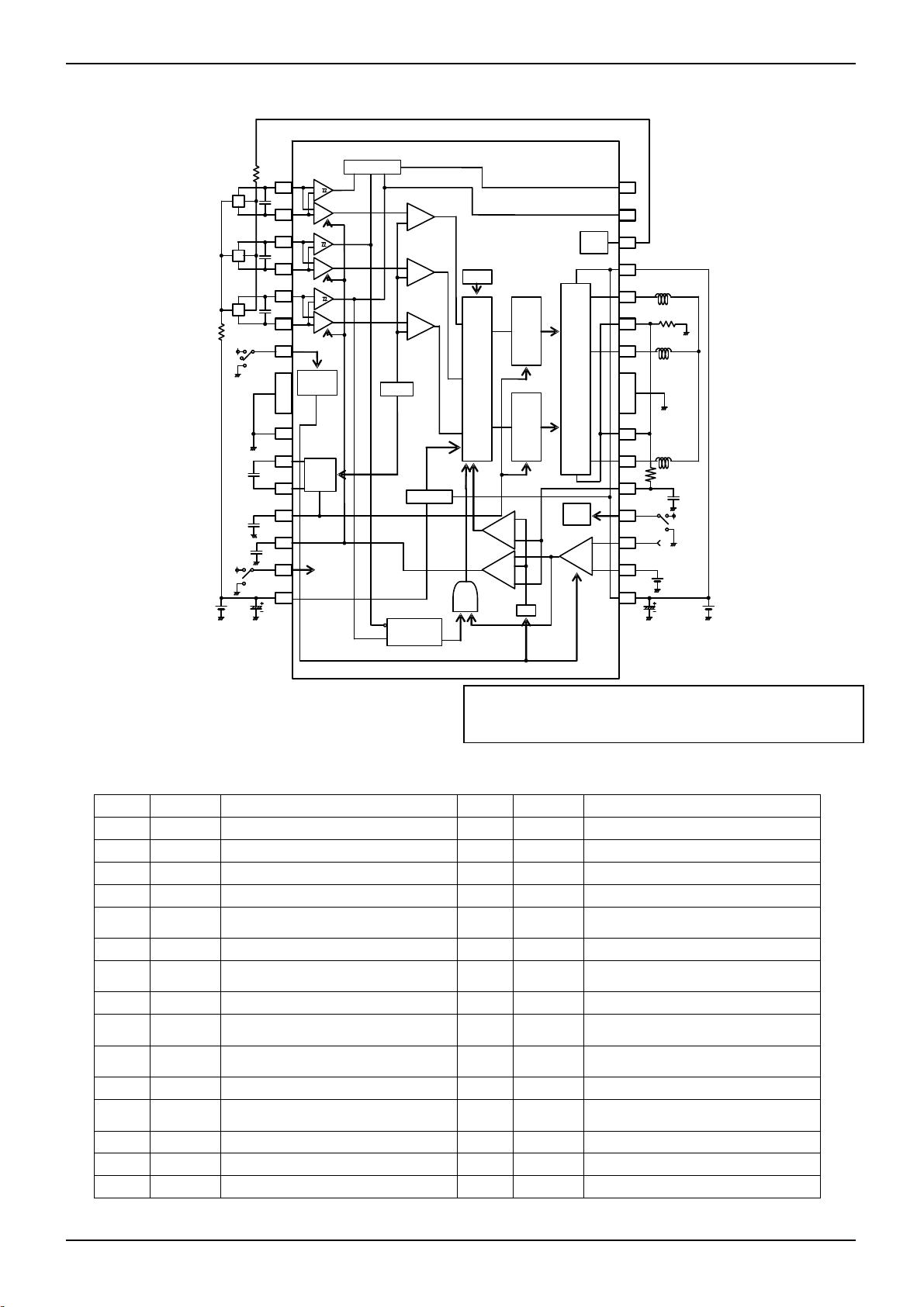
●Block Diagram, application Circuit Diagram and Pin Function
1) BA6859AFP-Y
Fig.4 BA6859AFP-Y Block Diagram
BA6859AFP-Y Pin Function Table
Pin No. Pin name Function
1 N.C. N.C.
2 N.C. N.C.
3 N.C. N.C.
Pd (W)
2.0
1.45
1.0
0
* Reduced by 11.6 mW/℃ over 25℃, when mounted on a glass epoxy
25 85
Fig.5 Power Dissipation Reduction (BA6859AFP-Y)
board (70 mm x 70 mm x 1.6 mm).
100 50 75 150
125
Ta(℃)
4 A3 Output pin
5 A2 Output pin
6 A1 Output pin
7 GND GND pin
8 H1+ Hall signal input pin
9 H1- Hall signal input pin
10 H2+ Hall signal input pin
11 H2- Hall signal input pin
12 H3+ Hall signal input pin
13 H3- Hall signal input pin
14 VH Hall bias input pin
15 BR Brake mode selection pin
16 CNF
17 SB Short brake pin
18 FR Rotation detection pin
19 ECR Output voltage control reference pin
20 EC Output voltage control pin
21 PS Power-saving pin
22 FG FG signal output pin
23 VCC Power supply pin
24 VM Motor power supply pin
25 RNF
FIN FIN GND
Capacitor connection pin for phase
compensation
Resistance connection pin for output
current detection
Technical Note
www.rohm.com
© 2010 ROHM Co., Ltd. All rights reserved.
5/17
2010.06 - Rev.
BA6859AFP-Y,BA6664FM,BD6671FM
A
r
2) BA6664FM
Hall1
Hall1
Hall1
Output to the motor will be opened at a chip tempe
175°C (Typ.). Do not use the IC in excess of a chip
rature of temperature of 150°C.
A3
2
A2
4
A1
7
HALL AMP
GND
8
H1+
9
-
H1
10
H2+
11
H2-
12
H3+
13
-
H3
14
Output will be open when the reverse rotation of the motor is
detected.
DRIVER
GAIN
CONTROL
CURRENT
TL
+
-
+
-
+
-
+
-
+
-
+
-
SENSE AMP
D Q
CK
TSD
GAIN
SWITCH
VCC
-+
PS
TORQUE
SENSE AMP
VCC
VCC
R
-
SHORT BRAKE
Q
BRAKE MODE
FIN
Torque limit current and I/O gain settings are made by
the RNF resistance value.
Resistance of 0.4 to 1.0Ω is recommended.
0.5Ω
RNF
28
RNF
VM
27
GSW
26
VCC
25
FG
24
PS
23
EC
22
ECR
21
FR
20
FG2
19
SB
18
CNF
17
BR
16
VH
15Hall Bias
500Ω
0.1µF
V
M
+
1µF
-
SERVO
SIGNAL
500Ω
Capacitor for noise level mitigation.
The recommended value is 0.47 µF to 10 µF.
+
1µF
-
I/O gain
Speed detection is attained by FG signal output.
The power saving mode is turned ON by low-level voltage,
and the circuit current and motor output will stop.
The motor torque current is controllable.
If the ECR voltage is set between 1.6 and 2.2V, the
maximum torque limit current will be obtained.
The detection of motor rotation direction is possible.
The short brake is operated regardless of brake mode settings.
Connect a capacitor for phase compensation.
The recommended value is 0.1µF.
Short brake and reversed brake settings are possible.
Resistor for setting Hall input level .
The recommended value is 200 Ω to 1k Ω.
Fig.6 BA6664FM Block Diagram
BA6664FM Pin Function Table
Pin No. Pin name Function
1 N.C. N.C.
2 A3 Output pin
3 N.C. N.C.
4 A2 Output pin
5 N.C N.C.
6 N.C. N.C.
7 A1 Output pin
Pd[W]
8 GND GND pin
9 H1+ Hall signal input pin
10 H1- Hall signal input pin
2.2
2.0
11 H2+ Hall signal input pin
12 H2- Hall signal input pin
13 H3+ Hall signal input pin
14 H3- Hall bias input pin
15 VH Hall bias input pin
16 BR Brake mode pin
Capacitor connection pin for phase
compensation
1.0
17 CNF
18 SB Short brake pin
19 FG2 FG 3-phase component output pin
20 FR Rotation detection pin
0 25 50 75 100 125 150
85
Ta(℃)
21 ECR Output voltage control reference pin
22 EC Output voltage control pin
23 PS Power-saving pin
Fig.7 Power Dissipation Reduction (BA6664FM、BD6671FM)
* Reduced by 11.6 mW/℃ over 25℃, when mounted on a glass epoxy board
(70 mm x 70 mm x 1.6 mm).
24 FG FG signal output pin
25 VCC Power supply pin
26 GSW Gain switching pin
27 VM Motor power supply pin
28 RNF
Resistance connection pin fo
current detection
FIN FIN GND
Technical Note
output
www.rohm.com
© 2010 ROHM Co., Ltd. All rights reserved.
6/17
2010.06 - Rev.
BA6859AFP-Y,BA6664FM,BD6671FM
A
3)BD6671FM
0.1 µ F
0.1 µF
0.047µF
200Ω
H1
1000pF
H2
1000pF
H3
200Ω
Vcc
Vcc
10µ F
1000pF
MODE
H1+
H1-
H2+
H2-
H3+
H3
GSW
FIN
GND
CP1
CP2
VG
CNF
Vcc
-
Hall comp
+
-
Hall Amp
+
-
+
-
Gain
control
Charge
Pump
Matrix
EXOR
+
+
-
+
-
+
-
OSC
D Q
CK QB
PWM
Comp
UVLO
Current Limit Comp
TSD
Matrix
Current
Sense AMP
REVERSE
DETECT
+
-
+
-
U-Pre
Driver
L-Pre
Driver
CL
Driver
Torque
AMP
PS
FG3
FG
VH
Hall
bias
VM
A1
RNF
A2
FIN
RNF1
A3
RNF2
PS
EC
+
ECR
-
VM
※ 1 Set capacitor between VM and GND, close as possible to the IC.
※2 To prevent from concentration of current routes, make the wiring
impedance values from the power supply equal as possible.
Fig.8 BD6671FM Block Diagram
BD6671FM Pin Function
Pin No Pin name Function Pin No Pin name Function
1 H1+ Hall signal input pin 15 VM Motor power supply pin
2 H1- Hall signal input pin 16 ECR Output voltage control reference pin
3 H2+ Hall signal input pin 17 EC Output voltage control pin
4 H2- Hall signal input pin 18 PS Power-saving pin
5 H3+ Hall signal input pin 19 RNF2
Resistance connection pin for output
current detection
6 H3- Hall signal input pin 20 A3 Output pin
7 GSW Gain switching pin 21 RNF1
Resistance connection pin for output
current detection
8 GND GND 22 A2 Output pin
9 CP1
10 CP2
Charge pump capacity connection
pin 1
Charge pump capacity connection
pin 2
23 RNF1
24 A1 Output pin
Resistance connection for output
current
11 VG Charge pump output pin 25 VM Motor power supply pin
12 CNF
Capacitor connection pin for phase
compensation
26 VH Hall bias pin
13 MODE Brake mode switching pin 27 FG FG Output pin
14 VCC Power supply pin 28 FG3 FG3 Output pin
FIN FIN GND
*Heat radiation FIN: GND
0.5
10kΩ
servo
signal
100µ F
※
2
※
Ω
1.65V
1
Technical Note
0.01µF
Vcc
www.rohm.com
© 2010 ROHM Co., Ltd. All rights reserved.
7/17
2010.06 - Rev.

BA6859AFP-Y,BA6664FM,BD6671FM
A
●I/O logic
1) BA6859AFP-Y
Input conditions
Pin. No 8 9 10 11 12 13 6 5 4 6 5 4
H1 + H1 - H2 + H2 - H3 + H3
1 L M H M M M H L L L H H
Output conditions
Forward rotation Reverse rotation
A1 A2 A3 A1 A2 A3
-
Technical Note
2) BA6664FM
2 H M L M M M L H H H L L
Input voltage
3 M M L M H M L H L H L H
4 M M H M L M H L H L H L
5 H M M M L M L L H H H L
6 L M M M H M H H L L L H
Note: Forward rotation EC<ECR
Reverse rotation EC>ECR
Input conditions
Forward rotation Reverse rotation
Output conditions
Pin. No 9 10 11 12 13 14 7 4 2 7 4 2
H1 + H1 - H2 + H2 - H3 + H3
A1 A2 A3 A1 A2 A3
-
1 L M H M M M H L L L H H
2 H M L M M M L H H H L L
Input voltage
3 M M L M H M L H L H L H
4 M M H M L M H L H L H L
5 H M M M L M L L H H H L
Hi=2.6V
Mid=2.5V
Low=2.4V
Hi=2.6V
Mid=2.5V
Low=2.4V
3)BD6671FM
6 L M M M H M H H L L L H
Note: Forward rotation EC<ECR
Reverse rotation EC>ECR
Output conditions
Input conditions
Forward rotation
Reverse rotation
(MODE=L)
Reverse rotation
(MODE=H)
Pin. No 1 2 3 4 5 6 24 22 20 24 22 20 24 22 20
H1 + H1 - H2 + H2 - H3 + H3
A1 A2 A3 A1 A2 A3 A1 A2 A3
-
1 L M H M M M H L L L H H L L L
2 H M L M M M L H H H L L L L L
Input voltage
3 M M L M H M L H L H L H L L L
4 M M H M L M H L H L H L L L L
5 H M M M L M L L H H H L L L L
6 L M M M H M H H L L L H L L L
Note: Forward rotation EC<ECR
Reverse rotation EC>ECR
Hi=2.6V
Mid=2.5V
Low=2.4V
www.rohm.com
© 2010 ROHM Co., Ltd. All rights reserved.
8/17
2010.06 - Rev.
BA6859AFP-Y,BA6664FM,BD6671FM
A
●I/O Timing Chart
1) BA6859AFP-Y, BA6664FM
2) BD6671FM
H1+
H2+
H3+
A1
Output current
H1 - + H2+
A1
Output current
A2
Output current
H2 - + H3+
A2
Output current
A3
Output current
H3 - + H1+
A3
Output current
A1 Output current
A1 Output voltage
A2 Output voltage
A2 Output current
H1+
H2+
H3+
30
30°
Technical Note
Fig. 9
°
Fig. 10
www.rohm.com
© 2010 ROHM Co., Ltd. All rights reserved.
9/17
2010.06 - Rev.

BA6859AFP-Y,BA6664FM,BD6671FM
A
●I/O Circuit
1) BA6859AFP-Y
(1) Power saving (pin 21) (6) FG output (pin 22)
21
Torque command input (pin 19, pin 20)
(2)
20
Coil output (A1: pin 6, A2: pin 5, A3: pin 4)
(3)
Hall input (H1+ : 8 pin, H1- : 9 pin, H2+ : 10 pin,
(4)
H2- : 11 pin, H3+ : 12 pin, H3- : 13 pin)
Hall bias(14 pin)
(5)
1kΩ
1KΩ
15KΩ
6
10KΩ
100KΩ
1kΩ
RNF
5
4
14
19
VM
External RNF Register
GND
1KΩ
VCC
(7) FR output (pin 18)
30kΩ
(8)
Short brake (17 pin)
(9) Brake mode (15 pin)
15
10kΩ
15kΩ
10kΩ
18
22
Technical Note
13kΩ 500Ω 500Ω 10kΩ
12kΩ 5kΩ 1kΩ
17
www.rohm.com
© 2010 ROHM Co., Ltd. All rights reserved.
10/17
2010.06 - Rev.

BA6859AFP-Y,BA6664FM,BD6671FM
A
2) BA6664FM
(1) Power saving (23 pin) (7) FG output (19 pin)
23
15KΩ
10KΩ
VCC
Torque command input (21 pin, 22 pin)
(2)
(8) FR output (20 pin)
22
1kΩ
1kΩ
21
VCC
(3)
Coil output (A1 : 7 pin, A2 : 4 pin, A3 : 2 pin)
7
4
VM
External RNFRegister
RNF
2
Short Brake mode (18 pin)
(9)
(4) Hall input (H1+ : 9 pin, H1- : 10 pin, H2+ : 11 pin,
H2- : 12 pin, H3+ : 13 pin, H3- : 14 pin)
1KΩ
1KΩ
(10)Brake mode (16 pin)
Hall bias (15 pin)
(5)
15
16
(11)
Gain switch (26 pin)
FG output (24 pin)
(6)
VCC
100KΩ
26
100KΩ
1KΩ
30KΩ
10kΩ
24
Technical Note
5kΩ
19
30kΩ
20
13kΩ 500Ω 500Ω 10kΩ
18
12kΩ 5kΩ 1kΩ
15kΩ
10kΩ
5KΩ
5KΩ
56KΩ
www.rohm.com
© 2010 ROHM Co., Ltd. All rights reserved.
11/17
2010.06 - Rev.

BA6859AFP-Y,BA6664FM,BD6671FM
A
1K
Ω
Technical Note
3) BD6671FM
(1) Hall input (H1 : 1 pin, H1-: 2 pin, H2+ : 3 pin, (6) Brake mode selection pin (13 pin)
H2- : 4 pin, H3+ : 5 pin, H3- : 6 pin)
Hn
+
VCC
1KΩ
VCC
Hn
-
13
VCC
30KΩ
20KΩ
1KΩ 1KΩ
25KΩ
(2) Gain switch (7pin) (7) Torque amp (ECR : 16 pin, EC : 17 pin)
VCC
7
1KΩ
VCC
75KΩ
100KΩ
10KΩ
10KΩ
25KΩ
VCC
16,17 1KΩ
(3)CP1 output (9pin) (8) Power saving (18 pin) (9)RNF2(19 pin)
VCC VCC
VCC
VCC
50Ω
9
18
30KΩ
20KΩ
19
1KΩ
(4) CP2 / VG output (CP2 : 10 pin, V
: 11 pin) (10) Output pin (A1 : 24 pin, A2 : 22 pin, A3 : 20 pin)
G
VM
50Ω
11
V
M
50Ω
10
24 22
20
RNF1
(5) CNF pin (12 pin) (11) Hall bias (26 pin) (12) FG / FG3 output (FG : 27 pin, FG3 : 28 pin)
VCC
VCC
VCC
VCC
12
50Ω
26
50Ω
27,28
2KΩ
100KΩ
710Ω
www.rohm.com
© 2010 ROHM Co., Ltd. All rights reserved.
12/17
2010.06 - Rev.

BA6859AFP-Y,BA6664FM,BD6671FM
A
Technical Note
●Operation Explanation
●Torque Command
Rotation direction
EC<ECR Forward
EC>ECR Reverse*
*Stops after detecting reverse rotation
R
[V]
Forward
NF
Offset voltage -
Offset voltage +
The I/O gain G
by the RNF detection resistor.
①(BA6859AFP-Y)
G
=0.35/RNF [A/V] ・・・・・(1)
EC
from the EC pin to the RNF pin (output current) is determined
EC
②(BA6664FM)
G
=0.325/RNF [A/V] (GSW=L)
ECL
=0.60/RNF [A/V] (GSW=OPEN)
G
3mV
1.65(ECR)
Fig.11
E
[V]
C
ECM
G
=1.4/RNF [A/V] (GSW=H)
ECH
③(BD6671FM)
=0.175/RNF [A/V] (GSW=L)
G
ECL
=0.35/RNF [A/V] (GSW=M)
G
ECM
G
=0.70/RNF [A/V] (GSW=H)
ECH
④The following torque limit current ITL is obtained (BA6859AFP-Y, BA6664FM)
ITL=0.35/RNF [A]・・・・・・・・・・・・・・・・・・・(2)
⑤(BD6671FM)
I
=0.2/RNF [A] (GSW=L)
TLL
=0.4/RNF [A] (GSW=M)
I
TLM
I
=0.6/RNF [A] (GSW=H)
TLH
The value will become smaller than the computed value due to the wiring
capacity and other factors, if the RNF resistance is 0.5Ω or below.
●Set-up of Motor Rotation Direction and Voltage Range of Torque Control Reference Terminal.
The motor rotation direction determined by the torque control terminal voltage EC and the torque control reference terminal
voltage ECR
Torque control input voltage Rotation direction
EC<ECR Forward torque
EC>ECR Reverse torque
Io
ITL
Forward torque
Reverse torque
0.5 3.3 5.0
2.5
Fig.12
EC[V]
The relation between the input gain and torque limit current expressed as (1) and (2) discussed previously is only valid
when EC and ECR are within a range from 0.5V to 3.3V. Depending on how the torque control reference terminal voltage,
ECR is specified, there may be a case when the output current for the motor does not go up to the torque limit value.
Please be aware of this voltage range when specifying the ECR voltage.
For BA6859AFP-Y, BA6664FM and BD6671FM, 1.6V~2.2V is recommended.
If above conditions are understood, the voltage input range to the EC and ECR terminals can be from 0V to VCC.
●Power Saving
The input circuit specified in I/O circuit 1) BA6859AFP-Y (1) is used for power saving input.
The power saving pin has a temperature characteristic of approximately –5 mV/℃ and also the built-in resistors has a dispersion of 30%.
Keep the input voltage range in mind.
www.rohm.com
© 2010 ROHM Co., Ltd. All rights reserved.
13/17
2010.06 - Rev.

BA6859AFP-Y,BA6664FM,BD6671FM
A
Technical Note
●Reverse Rotation Detection Function
Actual motor rotation at reverse detection
H2+
H2-
H3
H3-
+
-
+
+
-
EC
ECR
D-FF
Q
D
CK
+
-
H:OUTPUT.OPEN
(HIGH-IMPEDANCE)
When the motor rotates in the reverse direction, the reverse rotation
detection function will operate and the output will be in an open state.
Fig.13
EC < ECR: Forward torque (forward rotation)
EC > ECR: Deceleration (forward rotation)
The motor rotates in a reverse direction with inertial force.
Fig. 13 shows the construction of the reverse rotation detection circuit.
・Forward rotation (EC<ECR)
Stop
Fig. 9 shows the phase relation of the H2+ and H3+ Hall input signals,
in which case the reverse rotation detection circuit will not work.
・Reverse rotation (EC>ECR)
The phase relation of the H2+ and H3+ signals are opposite to that when the motor is rotating in the forward direction.
Therefore, the reverse rotation detection circuit operates, and the output is turned off and open.
●FR Signal Output (BA6859AFP-Y, BA6664FM)
FR output signal pin outputs the FR signal of low(L) or high(H) after detecting the motor rotation direction.
Motor rotation direction FR signal output
Forward “H”
Reverse “L”
●Brake Mode Change (BA6664FM, BD6671FM)
By applying high-level voltage to the BR pin, the brake mode for the following condition can be changed: EC > ECR.
EC<ECR EC>ECR
BR
L Forward rotation Reverse rotation brake
H Forward rotation Short brake
When the BR pin is set to high level and used in short-brake mode, open the SB pin.
The BR pin has a temperature characteristics of approximately -5 mV/℃. Use the BR pin within the permissible input range.
●Short Brake (BA6859AFP-Y, BA6664FM)
OFF OFF OFF
ON ON ON
When the short-brake pin is set to high level, as shown in Fig.18, the output
transistor (3-phase) on the high side will be turned off and the output transistor
(3-phase) on the low side will be turned on. The short brake pin has a
temperature characteristic of approximately -5 mV/℃. Keep the input voltage
range (see Fig12) in mind.
MOTOR
Fig.14
●Hall Input
The Hall element allows both serial and parallel connections.
VCC
VCC
Set the Hall input voltage between 1.0 and 4.0 V. Compute the
resistance between the VH and VCC pins in consideration of the
H1
H3
H2 H1
H2
H3
flowing current of the Hall device.
15-pin (Hall Bias)
Parallel Connection
Fig.15
15-pin (Hall Bias)
Serial Connection
www.rohm.com
© 2010 ROHM Co., Ltd. All rights reserved.
14/17
2010.06 - Rev.

BA6859AFP-Y,BA6664FM,BD6671FM
A
Technical Note
●FG Signal Output / FG2 Signal Output
The FG signal output/FG2 signal output terminals are for detecting the motor rotation speed. The output frequency of FG2
signal is three times higher than the FG frequency signal output. So, it is suitable for the slow speed rotation detection.
However, due to the Hall device variation and other reasons, the duty cycle may not reach 50% in some instances.
H1+
H1-
H2+
H2-
H3+
H3-
H1
+
-
H2
+
-
H3
+
-
FG2
FG
Fig. 16
H1 waveform
waveform
H
2
waveform
H
3
FG waveform
FG2 waveform
●Notes for use
Fig. 17
(1) Absolute maximum ratings
This product is subject to a strict quality management regime during its manufacture. However, damage may result if
absolute maximum ratings such as applied voltage and operating temperature range are exceeded. Assumptions should
not be made regarding the state of the IC (short mode or open mode) when such damage is suffered. A physical safety
measure such as a fuse should be implemented when use of the IC in a special mode where the absolute maximum
ratings may be exceeded is anticipated.
(2) Connecting the power supply connector backward
Connecting the power supply connector backwards may result in damage to the IC. Insert external diodes between the
power supply and the IC's power supply pins as well as the motor coil to protect against damage from backward
connections.
(3) Power supply lines
As return of current regenerated by back electromotive force of motor happens, take steps such as putting capacitor
between power source and GND as an electric pathway for the regenerated current. Be sure that there is no problem with
each property such as emptied capacity at lower temperature regarding electrolytic capacitor to decide capacity value. If
the connected power supply does not have sufficient current absorption capacity, regenerative current will cause the
voltage on the power supply line to rise, which combined with the product and its peripheral circuitry may exceed the
absolute maximum ratings. It is recommended to implement a physical safety measure such as the insertion of a voltage
clamp diode between the power supply and GND pins.
(4) GND potential
Ensure a minimum GND pin potential in all operating conditions.
(5) Setting of heat
Take the power dissipation Pd) into account for practical application and make thermal design with sufficiently margined.
(6) Pin short and mistake fitting
Use caution when orienting and positioning the IC for mounting on printed circuit boards. Improper mounting may result
in damage to the IC. Shorts between output pins or between output pins and the power supply and GND pins caused by
the presence of a foreign object may result in damage to the IC.
(7) Actions in strong magnetic field
Use caution when using the IC in the presence of a strong magnetic field as doing so may cause the IC to malfunction.
www.rohm.com
© 2010 ROHM Co., Ltd. All rights reserved.
15/17
2010.06 - Rev.
BA6859AFP-Y,BA6664FM,BD6671FM
A
P
iti
Technical Note
(8) ASO
When using the IC, set the output transistor so that it does not exceed absolute maximum ratings or ASO.
(9) Thermal shutdown circuit (TSD)
This IC incorporates a TSD circuit. If the chip becomes the following temperature, coil output to the motor will be open.
The TSD circuit is designed only to shut the IC off to prevent runaway thermal operation. It is not designed to protect the
IC or guarantee its operation. Do not continue to use the IC after operating this circuit or use the IC in an environment
where the operation of the TSD circuit is assumed.
TSD ON temperature [℃] (typ.) Hysteresis temperature [℃] (typ.)
BA6859AFP-Y 175 25
BA6664FM 175 15
BD6671FM 170 25
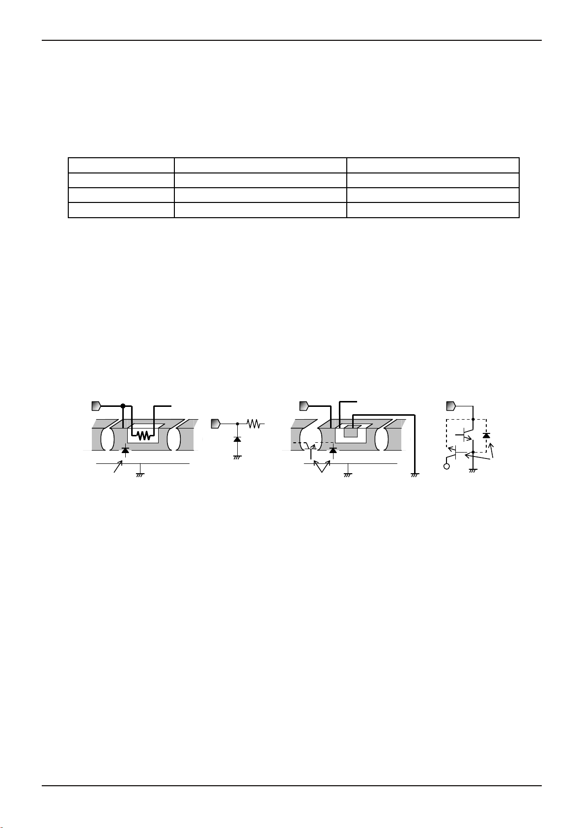
(10) Regarding input pin of the IC
This monolithic IC contains P+ isolation and P substrate layers between adjacent elements in order to keep them isolated.
P/N junctions are formed at the intersection of these P layers with the N layers of other elements to create a variety of
parasitic elements.
For example, when the resistors and transistors are connected to the pins as shown in Fig. 18,
○the P/N junction functions as a parasitic diode
when GND > (Pin A) for the resistor or GND > (Pin B) for the transistor (NPN).
○Similarly, when GND > (Pin B) for the transistor (NPN), the parasitic diode described above combines
with the N layer of other adjacent elements to operate as a parasitic NPN transistor.
The formation of parasitic elements as a result of the relationships of the potentials of different pins is an inevitable result
of the IC's architecture. The operation of parasitic elements can cause interference with circuit operation as well as IC
malfunction and damage. For these reasons, it is necessary to use caution so that the IC is not used in a way that will
trigger the operation of parasitic elements, such as by the application of voltages lower than the GND (P substrate)
voltage to input pins.
Pin A
+
P
P
N
P
GND
Resistor Transistor (NPN)
+
N N
P substrate
Pin A
aras
element
Pin B
+
P
N
c
Parasitic element
B
C
E
N
GND
P
P
P substrate
Pin B
+
N
GND
B C
E
GND
Other adjacent
elements
Fig.18 Example of IC structure
(11) Testing on application boards
When testing the IC on an application board, connecting a capacitor to a pin with low impedance subjects the IC to stress.
Always discharge capacitors after each process or step. Ground the IC during assembly steps as an antistatic measure,
and use similar caution when transporting or storing the IC. Always turn the IC's power supply off before connecting it to
or removing it from a jig or fixture during the inspection process.
(12) Ground Wiring Pattern
When using both small signal and large current GND patterns, it is recommended to isolate the two ground patterns,
placing a single ground point at the application's reference point so that the pattern wiring resistance and voltage
variations caused by large currents do not cause variations in the small signal ground voltage. Be careful not to change
the GND wiring pattern of any external parts, either.
Parasitic
element
www.rohm.com
© 2010 ROHM Co., Ltd. All rights reserved.
16/17
2010.06 - Rev.
BA6859AFP-Y,BA6664FM,BD6671FM
A
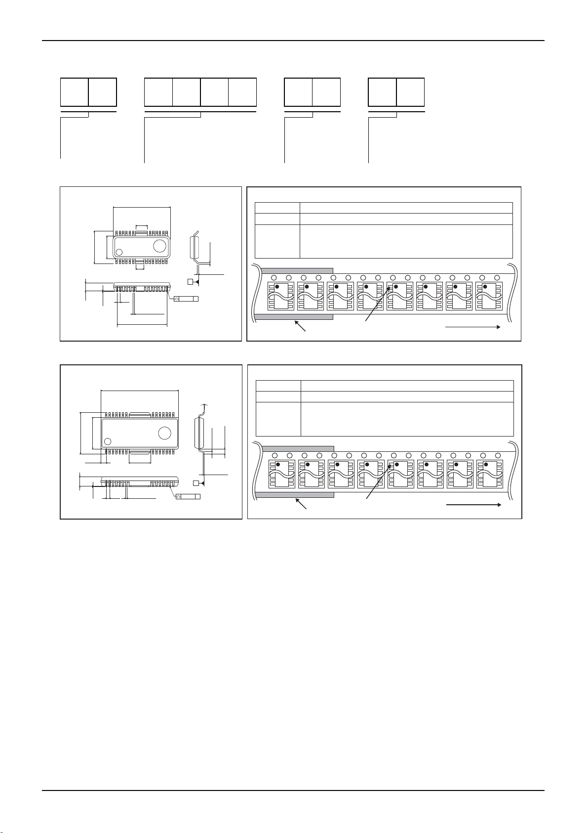
●Ordering part number
B A 6 6 6 4 F M - E 2
HSOP25
HSOP-M28
Part No.
BA
BD
1.9 ± 0.1
9.9± 0.3
7.5± 0.2
1.25
2.2± 0.1
0.11
Part No.
13.6 ± 0.2
(MAX 13.95 include BURR)
2.75 ± 0.1
25 14
7.8 ± 0.3
5.4 ± 0.2
1
1.95 ± 0.1
0.8
0.11
0.36 ± 0.1
12.0 ± 0.2
18.5± 0.2
(MAX 18.85 include BURR)
28
1
5.15± 0.1
0.37± 0.1
0.8
6859A
6664
6671
13
Package
FP-Y : HSOP25
FM : HSOP-M28
Packaging and forming specification
E2: Embossed tape and reel
<Tape and Reel information>
Embossed carrier tapeTape
Quantity
Direction
of feed
0.3Min.
0.25 ± 0.1
S
0.1 S
(Unit : mm)
<Tape and Reel information>
+6°
4°
0.1 S
0.27
S
(Unit : mm)
−4°
0.5± 0.2
+0.1
−0.05
1.2± 0.15
15
14
Quantity
Direction
of feed
2000pcs
E2
The direction is the 1pin of product is at the upper left when you hold
()
reel on the left hand and you pull out the tape on the right hand
Reel
Embossed carrier tapeTape
1500pcs
E2
The direction is the 1pin of product is at the upper left when you hold
()
reel on the left hand and you pull out the tape on the right hand
Reel
1pin
Order quantity needs to be multiple of the minimum quantity.
∗
1pin
Order quantity needs to be multiple of the minimum quantity.
∗
Technical Note
Direction of feed
Direction of feed
www.rohm.com
© 2010 ROHM Co., Ltd. All rights reserved.
17/17
2010.06 - Rev.

Notes
No copying or reproduction of this document, in part or in whole, is permitted without the
consent of ROHM Co.,Ltd.
The content specied herein is subject to change for improvement without notice.
The content specied herein is for the purpose of introducing ROHM's products (hereinafter
"Products"). If you wish to use any such Product, please be sure to refer to the specications,
which can be obtained from ROHM upon request.
Examples of application circuits, circuit constants and any other information contained herein
illustrate the standard usage and operations of the Products. The peripheral conditions must
be taken into account when designing circuits for mass production.
Great care was taken in ensuring the accuracy of the information specied in this document.
However, should you incur any damage arising from any inaccuracy or misprint of such
information, ROHM shall bear no responsibility for such damage.
The technical information specied herein is intended only to show the typical functions of and
examples of application circuits for the Products. ROHM does not grant you, explicitly or
implicitly, any license to use or exercise intellectual property or other rights held by ROHM and
other parties. ROHM shall bear no responsibility whatsoever for any dispute arising from the
use of such technical information.
Notice
The Products specied in this document are intended to be used with general-use electronic
equipment or devices (such as audio visual equipment, ofce-automation equipment, communication devices, electronic appliances and amusement devices).
The Products specied in this document are not designed to be radiation tolerant.
While ROHM always makes efforts to enhance the quality and reliability of its Products, a
Product may fail or malfunction for a variety of reasons.
Please be sure to implement in your equipment using the Products safety measures to guard
against the possibility of physical injury, re or any other damage caused in the event of the
failure of any Product, such as derating, redundancy, re control and fail-safe designs. ROHM
shall bear no responsibility whatsoever for your use of any Product outside of the prescribed
scope or not in accordance with the instruction manual.
The Products are not designed or manufactured to be used with any equipment, device or
system which requires an extremely high level of reliability the failure or malfunction of which
may result in a direct threat to human life or create a risk of human injury (such as a medical
instrument, transportation equipment, aerospace machinery, nuclear-reactor controller, fuelcontroller or other safety device). ROHM shall bear no responsibility in any way for use of any
of the Products for the above special purposes. If a Product is intended to be used for any
such special purpose, please contact a ROHM sales representative before purchasing.
If you intend to export or ship overseas any Product or technology specied herein that may
be controlled under the Foreign Exchange and the Foreign Trade Law, you will be required to
obtain a license or permit under the Law.
Thank you for your accessing to ROHM product informations.
More detail product informations and catalogs are available, please contact us.
ROHM Customer Support System
www.rohm.com
© 2010 ROHM Co., Ltd. All rights reserved.
http://www.rohm.com/contact/
R1010
A
 Loading...