

ROHM BA6665FM Datasheet
BA6665FM
Optical disc ICs
Motor driver for CD -ROMs
BA6665FM
The BA6665FM is a CD-ROM s pindle motor driv er suppo rting revers e-rota tion p reventing circuit. It i ncorpor ates po wer
save circuit, th ermal shut down circuit, FG output , hall bias, etc. The 3-phasef all-wave pseudo linear driving s ystem
achieves high-performance and multi-function.
z
zApplications
zz
CD-ROM / R W, D VD-ROM
z
zFeatures
zz
1) 3-phase, full-wave pseudo linear driving system
2) Built in power save
3) Built in thermal shut down circuit
4) Built in current limit circuit
5) Built in Hall Bias circuit
6) Built in FG-output ( 3 phase parallel output )
7) With switching function of regular / reverse rotations
z
zAbsolute maximum ratings (Ta=25°C)
zz
Parameter Symbol Limits Unit
V
Supply voltage
Supply voltage V
Power dissipation Pd
Operate.temp.range
Strage.temp.range
Juncition temp.
Maximum o.current
70mm×70mm×1.6mm glass epoxy board.
∗1 Derating in done at 17.6mW / ˚C for operating above Ta=25˚C.
∗2 Do not, however exceed Pd, ASO and Tj=150˚C.
zzzz
Recommended operating conditions
Parameter
Operating supply voltage
range
CC
M
Topr −20~+75
Tstg
Tjmax
I
OUT
(Ta=25°C)
Symbol Min. Typ. Max. Unit
CC
V
V
M
4.5 5.5−
3.0 14.0
7V
15
1
∗
2200
−55~+150
150
2
∗
1300
−
V
mW
˚C
˚C
˚C
mA
V
Optical disc ICs
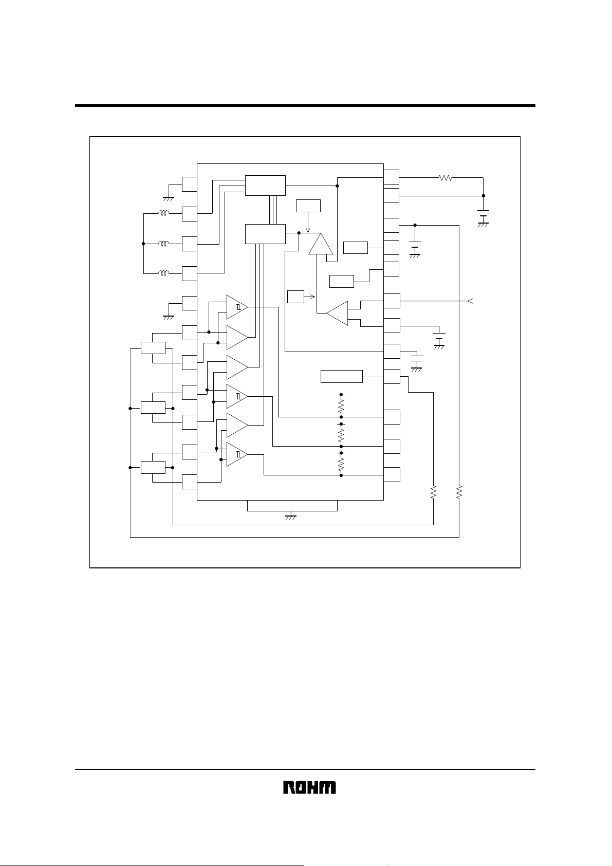
z
zBlock diagram
zz
BA6665FM
Hall 1
Hall 2
Hall 3
FIN
10
11
12
13
14
DRIVER
R
NF
27
28
3
GAIN
5
CONTROL
7
TSD
+
CURRENT
SENSE AMP
25
V
−
REV
24
CC
23
V
M
PS
8
9
+
−
+
−
TL
TORQUE
SENSE AMP
+
−
22
21
SERVO
SIGNAL
20
+
−
+
−
+
−
+
−
1.6kΩ
1.6kΩ
1.6kΩ
Hall Bias
VCC
(Typ.)
VCC
(Typ.)
VCC
(Typ.)
19
18
17
16
FIN

Optical disc ICs
z
zPin descriptions
zz
BA6665FM
Pin No. Function
10
11
12
13
14
15
16
17
18
19
20
21
22
23
24
25
26
27
28
FIN
Pin Name
N.C.1
2
3
4
5
6
7
8
9
N.C.
A
N.C.
A
N.C.
A
GND
1
H
H
1
H
2
H
2
H
3
H
3
3
2
1
+
−
+
−
+
−
N.C.
FG3
FG2
FG1
H
V
C
NF
E
CR
E
C
PS
R
EV
V
CC
N.C.
V
M
R
NF
FIN
N.C.
N.C.
Output3 for motor
N.C.
Output2 for motor
N.C.
Output1 for motor
GND
Hall input Amp1. positive input
Hall input Amp1. negative input
Hall input Amp2. positive input
Hall input Amp2. negative input
Hall input Amp3. positive input
Hall input Amp3. negative input
N.C.
FG3 signal output terminal
FG2 signal output terminal
FG1 signal output terminal
Hall bias
Capacitor connection pin for phase compensation
Torque control standard voltage input terminal
Torque control voltage input terminal
START / STOP switch
Reverse terminal
Power supply for signal division
N.C.
Power supply for driver
Terminal connection for current sensing resistor
GND
 Loading...