

1
Multimedia ICs
Vocal fader IC
BA3837 / BA3837F / BA3838F
The BA3837, BA3837F and BA3838F are ICs with an internal secondary active LPF for vocal cancellation functions
and mixing amplifier functions with high degrees of vocal cancellation. Three control pins are used to switch between
modes: the key controller input mode, through mode, vocal fader mode, sound multiplexing mode and mute mode.
By offering these functions on a single chip, these ICs can significantly reduce the number of external components.
•
Applications
Karaoke functions on stereo systems, portable stereos and VCRs
•
Features
•
Absolute maximum ratings (Ta = 25°C)
1) Single-chip IC with vocal fader, to erase vocals from
commercially available recordings.
2) Internal secondary active LPF for high degrees of
vocal cancellation (high synchronization rejection).
3) Three control pins for switching between 4 modes:
through, vocal fader, sound multiplexing and mute.
4) Key controller input and internal switches.
5) Low noise and low distortion.
6) Internal microphone mixing amplifier.
7) Available in two packages: DIP 16-pin and SOP 16pin (BA3838F is available in SOP 16-pin only).
Parameter Symbol Limits Unit
18 V
DIP16
Pd mV
SOP16
Topr °C
Tstg °C
V
CC
1000
∗
1
550
∗
2
– 40 ~ + 85
– 55 ~ + 125
Power supply voltage
Power
dissipation
Operating temperature
Storage temperature
∗
1 Reduced by 10 mW for each increase in Ta of 1°C over 25°C.
∗
2 Reduced by 5.5mW for each increase in Ta of 1°C over 25°C.
•
Recommended operating conditions (Ta = 25°C)
Parameter Symbol Min. Typ. Max. Unit
V
CC 5.4 — 10 V
V
CC 5.4 — 13 V
V
CC 4.0 — 15 V Ta = 25
°C
Ta = – 40°C ~ + 85°C
Ta = – 40°C ~ + 60°C
Conditions
Power supply voltage
∗
1
Power supply voltage
∗
1
Power supply voltage
∗
2
∗
2 BA3838F
∗
1 BA3837 and BA3837F
2
Multimedia ICs BA3837 / BA3837F / BA3838F
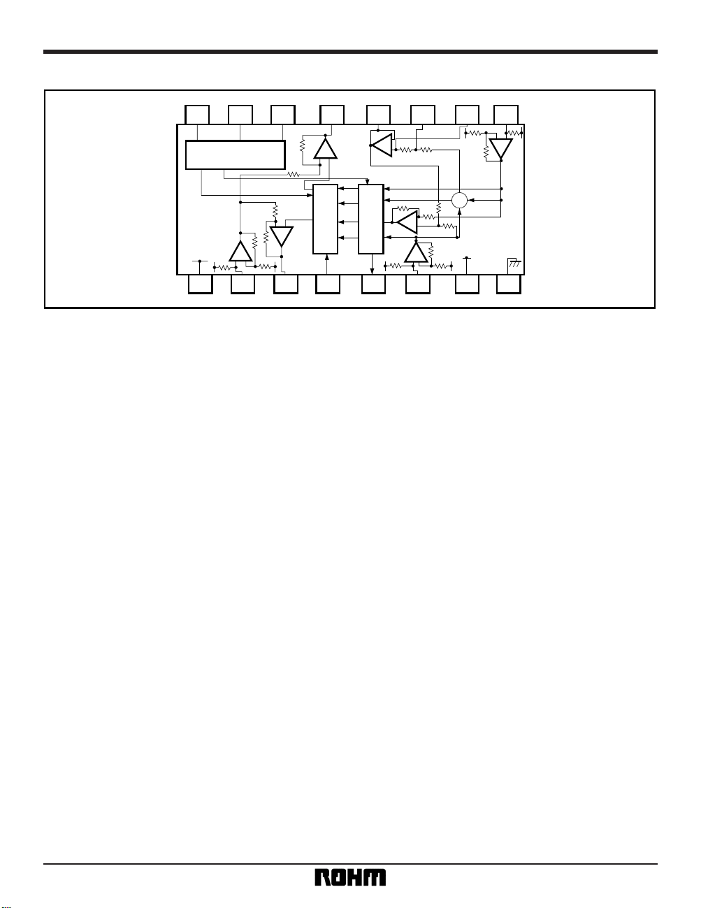
•
Block diagram
16 15 14 13 12 11 10 9
123456 78
LOGIC
SW2
SW1
R
L + R
L – R
L
+
+
–
–
+
–
+
+
–
–
+
–
+
–
+
V
CC MIC LOUT FK TK LIN BIAS GND
C B A ROUT LP LP LP RIN
3
Multimedia ICs BA3837 / BA3837F / BA3838F
•
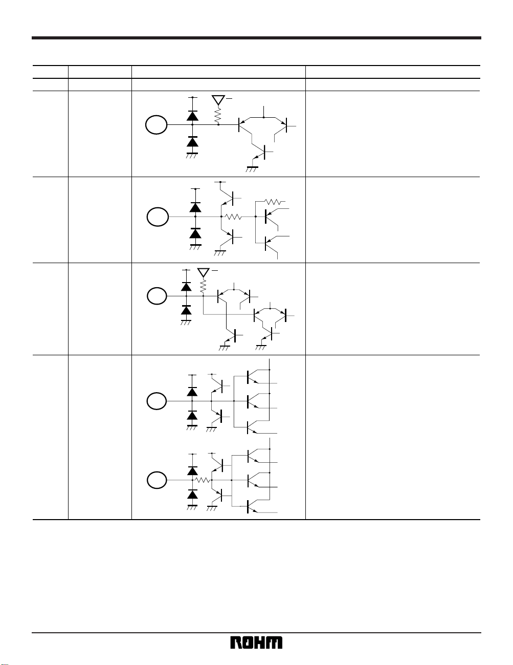
Pin descriptions
1V
CC
2 MIC IN
3LOUT
4FK
5TK
Pin No.
BA3837 / BA3837F
BA3838F
51k
20k
20k
51
k
400
5
5
4
3
2
V
CC
V
CC
V
CC
V
CC
V
CC
V
CC
V
CC
1
2
V
CC
1
2
V
CC
V
CC
Pin name Equivalent circuit Function
Mixing input pin for microphone sound
Lch output pin
Input pin for key controller signals
Output pin for key controller signals
4
Multimedia ICs BA3837 / BA3837F / BA3838F
LIN
8
9 RIN
10 LPF1
LPF2
6
7
11
BIAS
GND
Pin No.
6
7
9
10
11
10
11
51k
51k
51k
51k
10.4k
10.4k
10.4k
10.4k
V
CC
V
CC
V
CC
V
CC
V
CC
V
CC
1
2
V
CC
1
2
V
CC
Pin name Equivalent circuit
L signal input pin
Signal bias circuit pin
R signal input pin
Function
LPF time constant pin
LPF time constant pin

5
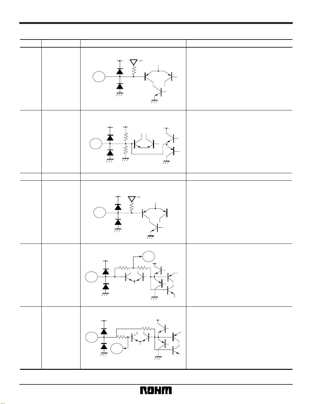
Multimedia ICs BA3837 / BA3837F / BA3838F
12
13 ROUT
14 CONTA
15 CONTB
16 CONTC
LPF3
Pin No.
12
20k
13
20k
20k
15
16
14
V
CC
V
CC
V
CC
V
CC
V
CC
V
CC
V
CC
V
CC
Pin name Equivalent circuit
LPF output pin
R output pin
Mode switching pin A
Mode switching pin B
Mode switching pin C
Function

6
Multimedia ICs BA3837 / BA3837F / BA3838F
Parameter Symbol Min. Typ. Max. Unit Conditions
I
Q
1.6 2.4 3.3 mA
V
om
2.3 2.8
—
G
VT
10 14 17 dB
G
VF
10 14 17 dB
G
VM
5 8 11 dB
CT 54 70
—
dB fIN =
1kHz
MU 73 80
—
dB fIN =
1kHz
SV 28 33
—
dB
THD
—
0.02 0.07 %
V
N
—
15 22
R
IN
35 50 65 k
Ω
VthH 4.7
——
V
VthL
—
—
0.3 V
∆
DC
—
726 mV
µ
Vrms
Vrms
—
—
—
Quiescent current
Maximum output voltage
L / R gain
Low frequency gain
Microphone gain
Crosstalk
Mute attenuation
Vocal suppression rate
Total harmonic distortion
Noise level
Input impedance
Output switching DC differential
Control pin threshold (high)
Control pin threshold (low)
䊊
Not designed for radiation resistance.
Through mode
THD
=
1%, through mode
Through mode
fin
=
50kHz, vocal fader mode
Vocal fader mode
Through mode, BW
:
400Hz - 30kHz
R
g
=
0, DIN AUDIO
LIN, RIN, MICIN, FK
Maximum output voltage differential between L, R and TK modes
0 : 0V 1 : 5V
A B C LOUT ROUT TK
0 0 0 MUTE MUTE MUTE
0 0 1 VF VF VF
0 1 0 L L L
0 1 1 L R L
1 0 0 MUTE MUTE MUTE
•
•
•
•
1 0 1 KC KC VF
1 1 0 KC KC L
1 1 1 KC KC L + R
—
—
—
—
Mute
Vocal fader mode
Sound multiplexing mode
Through mode
Mute
Vocal fader mode
Sound multiplexing mode
L + R
Key controller modeMode
VF : vocal fader output
KC : signal passed through key controller
1. L / R input and output in the through mode are synchronous with a gain of 14dB.
2. L / R input and TK output in the key controller mode are synchronous with a gain of 8dB.
3. FK input and L / R output in the key controller mode are synchronous with a gain of 6dB.
4.MIC input and L / R output are negative phase with a gain of 8dB.
(1) Microphone output is not muted during muting (ABC = 000 or 100).
(2) Gain and relative phase: See block diagram.
Mode table (A = pin14, B = pin15, C = pin16)
•
Electrical characteristics
BA3837 / F (unless otherwise noted, Ta = 25°C, Vcc = 10V, f
IN = 1kHz, VIN = 150mV, RL = 100kΩ)

7
Multimedia ICs BA3837 / BA3837F / BA3838F
BA3838F (unless otherwise noted, Ta = 25°C, Vcc = 10V, fIN = 1kHz, VIN = 150mV, Rl = 100Ω)
Parameter Symbol Min. Typ. Max. Unit Conditions
I
Q
1.9 2.7 3.6 mA
V
om
2.3 2.8
—
Vrms
G
VT
10 14 17 dB
G
VF
10 14 17 dB
G
VM
5 8 11 dB
CT 54 70
—
dB fIN =
1kHz
SV 28 33
—
dB
THD
—
0.02 0.07 %
V
N
—
15 22µVrms
R
IN
35 50 65 kΩLIN, RIN, MICIN, FK
VthH 4.7
——
V
VthL
——
0.3 V
∆
DC
—
746mV
—
—
—
Quiescent current
Maximum output voltage
L / R gain
Low frequency gain
Microphone gain
Crosstalk
Vocal suppression rate
Total harmonic distortion
Noise level
Input impedance
Control pin threshold (high)
Output switching DC differential
䊊
Not designed for radiation resistance.
Control pin threshold (low)
Through mode
THD
=
1%, through mode
fin
=
50kHz, vocal fader mode
Vocal fader mode
Maximum output voltage differential between L, R and TK modes
R
g
=
0, DIN AUDIO, through mode
Through mode
Through mode, BW
:
400Hz - 30kHz
0 : 0V 1 : 5V
A B C LOUT ROUT TK
0 0 0
0 0 1 VF VF VF
0 1 0 L L L
0 1 1 L R L
1 0 0
•
1 0 1 KC KC VF
•
1 1 0 KC KC L
•
1 1 1 KC KC L + R
•
KC
RRKCR
R
—
—
—
—
1. Gain of L / R input and output in the through mode: 14 dB (synchronous)
2. Gain of L / R input and TK output in the key controller mode: 8dB (synchronous)
3. Gain of FK input and L / R output in the key controller mode: 6dB (synchronous)
4. MIC input and L / R output are negative phase with a gain of 8dB.
∗
Gain and relative phase: See block diagram.
VF : vocal fader output
KC : signal passed through key controller
Vocal fader mode
Through mode
Vocal fader mode
L + R
Sound multiplexing mode (ROUT)
Sound multiplexing (LOUT)
Sound multiplexing (R)
Sound multiplexing mode (L)
Mode Key controller mode
Mode table (A = pin14, B = pin15, C = pin16)

8
Multimedia ICs BA3837 / BA3837F / BA3838F
A
A
A
A
V
V
4.7V
0.3V
100k
AUDIO
ANALYZER
MEASUREMENT
600Ω
OSC
51k
MIC
FK
L
10µ
+
10µ 10µ 10µ 22µ
C1 C2 C3 C4
++ ++
C7
0.22µ
0.047µ
C5
C6
10µ
+
16 15 14 13 12 11 10 9
12 34567 8
C B A Rout LP LP LP RIN
V
CC MICIN Lout FK TK LIN BIAS GND
R
Fig. 1
•
Measurement circuit (BA3838F)

9
Multimedia ICs BA3837 / BA3837F / BA3838F
µ – CON
51k 51k 51k
1µ 1µ 1µ
+++
0.22µ
0.047µ
10µ
+
TAPE, CD
LD, etc.
10µ
+
+
22µ
Key
– con
10µ
+
POWER
AMP
MICROPHONE
MICROPHONE
+
16 15 14 13 12 11 10 9
12345678
Fig. 2
•
Application example (BA3838F)

•
Operation notes
(1) The example in the diagram “Application example”
is recommended with confidence. However, be
sure to comply with these precautions and verify
characteristics during actual use. Also, when
changing an attached circuit constant, be sure to
allow sufficient margins by taking into account both
static and transient characteristics, including variation in these ICs and the attached components.
(2) The low pass filter cutoff frequency is determined
by the internal circuitry and by C
6 and C7 in Fig. 1.
With the constant used in Fig. 1, the cutoff frequency (fc) is roughly 150Hz. This cutoff frequency can be changed by changing C
6 and C7. When
C
6 is multiple a, and C7 is multiple b, respectively,
the cutoff frequency is calculated thus:
(3) For the gain and relative phase of the input pin
(LIN, RIN, MICIN and FK) inputs and output pin
(LOUT, ROUT and TK) outputs, refer to “Gain and
relative phase,” on page 2 / 10.
(4) Electrical characteristics are measured at a load
resistance (R
L) of roughly 100kΩ. As using an
extremely low load resistance (below 10kΩ) will
result in slight variation in maximum output voltage
and total harmonic distortion, caution must be
used when designing connections with the subsequent stage.
(5) The pin 7 bias voltage is roughly Vcc / 2. Because
this is also the input and output pin voltage, select
coupling capacitor polarity according to relative
potential and the characteristics of the components to which the coupling capacitor is to be connected.
(6) When outputting L + R from LOUT and ROUT in
an application in which the key controller is left
unconnected, attach a 10µF electrolytic capacitor
between pins 4 and 5, with pin 5 being positive (L
+ R mode: ABC = 111).
(7) Connecting a capacitance load to pin 5 (TK) of
BA3837 / F can worsen noise characteristics.
When connecting a capacitance load higher than
10µF, insert 1kΩ in series (Figs. 1 and 2). The pin
5 output impedance is roughly 5Ω (1kHz). In the
BA3838F it is roughly 400Ω (1kHz).
(8) The vocal fader works by canceling out the syn-
chronous component of the signal, leaving the low
components in place. Consequently, the vocal
fader may not be very effective with certain
recordings.
(9) In cases where output DC differential can cause
noise when switching between modes, use a time
constant for the timing of control pin switching, or
take some other measure.
(10) Operating supply voltage may vary according to
ambient temperature. Using this IC outside the
recommended supply voltage range may result in
increased crosstalk or mute attenuation.
10
Multimedia ICs BA3837 / BA3837F / BA3838F
QUIESCENT CURRENT : IQ (mA)
POWER SUPPLY VOLTAGE : VCC (V)
0 2 4 6 8 101214161820
4
3
2
1
5
Fig. 3 IQ vs. VCC characteristics
(BA3837 / F)
QUIESCENT CURRENT : IQ (mA)
POWER SUPPLY VOLTAGE : VCC (V)
02468101214161820
4
3
2
1
5
Fig. 4 IQ vs. VCC characteristics
(BA3838F)
FREQUENCY : f (Hz)
VOCAL COMRESSION RATIO : SV (dB)
10 100 1K
10K 100K
40
20
14
0
– 20
– 40
– 60
Fig. 5 SV vs. frequency
characteristics
•
Electrical characteristic curves
The value of Q is: Q =
(Currently, Q ⱌ 1)
12C7
C6
150
ab
(Hz)
fc =

11
Multimedia ICs BA3837 / BA3837F / BA3838F
TOTAL HARMONIC DISTORTION : THD (%)
INPUT LEVEL : VIN (dBV)
L,R OUTPUT
– 40 – 30 – 20
– 10 0
10
10
1
0.1
0.01
0.001
Fig. 6 THD vs.
V
IN characteristics
•
External dimensions (Units: mm)
DIP16
BA3837
SOP16
BA3837F / BA3838F
0.51Min.
0.3
± 0.1
916
81
6.5
± 0.3
3.2 ± 0.2
4.25 ± 0.3
0.5
± 0.1
19.4 ± 0.3
2.54
0° ~ 15°
7.62
0.4 ± 0.11.27
0.15
0.15 ± 0.1
0.3Min.
4.4 ± 0.2
6.2 ± 0.3
0.11
1.5 ± 0.1
1
16
10.0 ± 0.2
8
9
 Loading...