

Page 1
Regulator ICs
Dual circuit, variable output voltage
regulator
BA3960
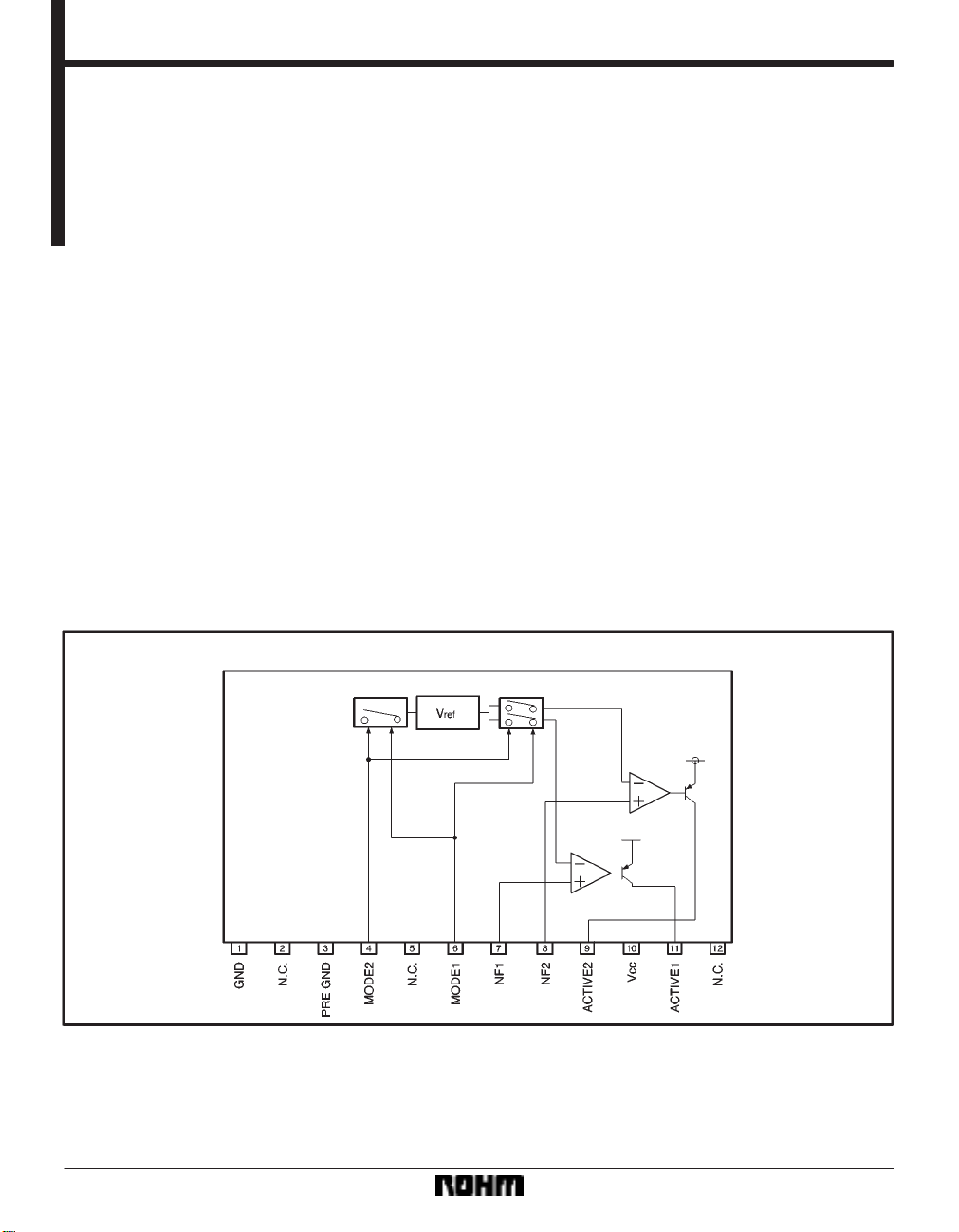
The BA3960 is a dual circuit, variable output, series regulator. PNP output transistors allow minimum voltage differential
between input and output. Each of the two circuits can be turned on or off independently by using the system logic control.
When both circuits are off, the IC keeps a standby state with no supply current.
Applications
Audio and video systems, CD and CD-ROM systems, computer peripheral devices, industrial equipment
Features
1) Containing two circuits of variable-output series regulator.
2) PNP output transistor characterized by low saturation voltage.
3) Logic control allowing ON/OFF switching of output.
4) No supply current when both circuits are off.
5) Output current limit circuit protects the IC against
short-circuiting damage.
6) Compact HSIP-B12 package allows a large power
dissipation.
7) Thermal protection circuit prevents heat damage to
the IC.
Block diagram
136
Page 2
Regulator ICs BA3960
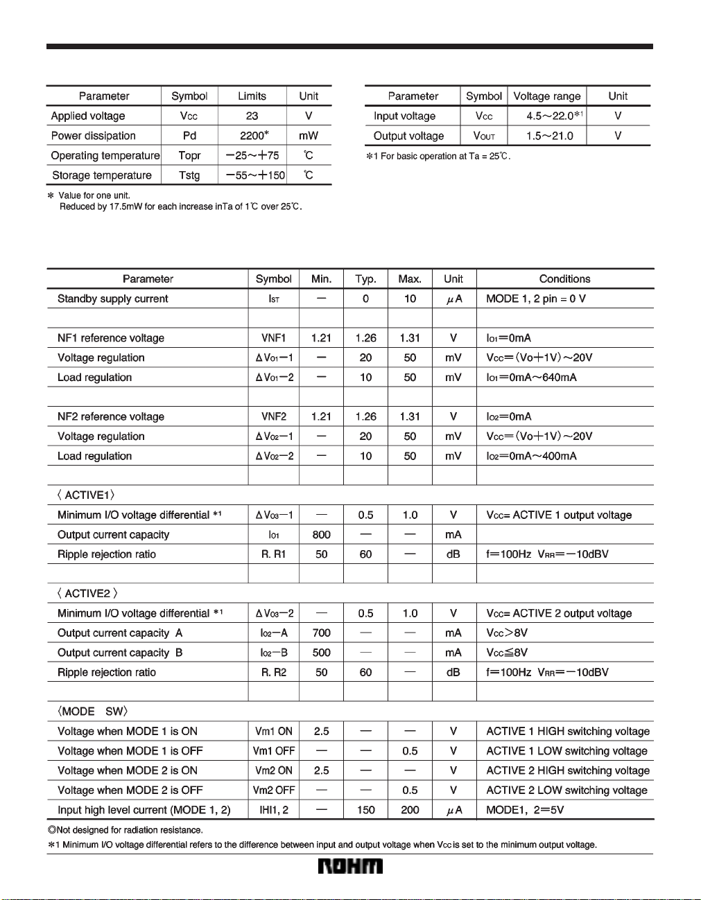
FAbsolute maximum ratings (Ta = 25_C) FRecommended operating conditions
FElectrical characteristics
(unless otherwise noted, Ta = 25_C, V
and R12, R22=3.9kΩ)
CC = 12.0V, ACTIVE 1 : IO = 640mA, ACTIVE 2 : IO = 400mA
137
Page 3
Regulator ICs BA3960
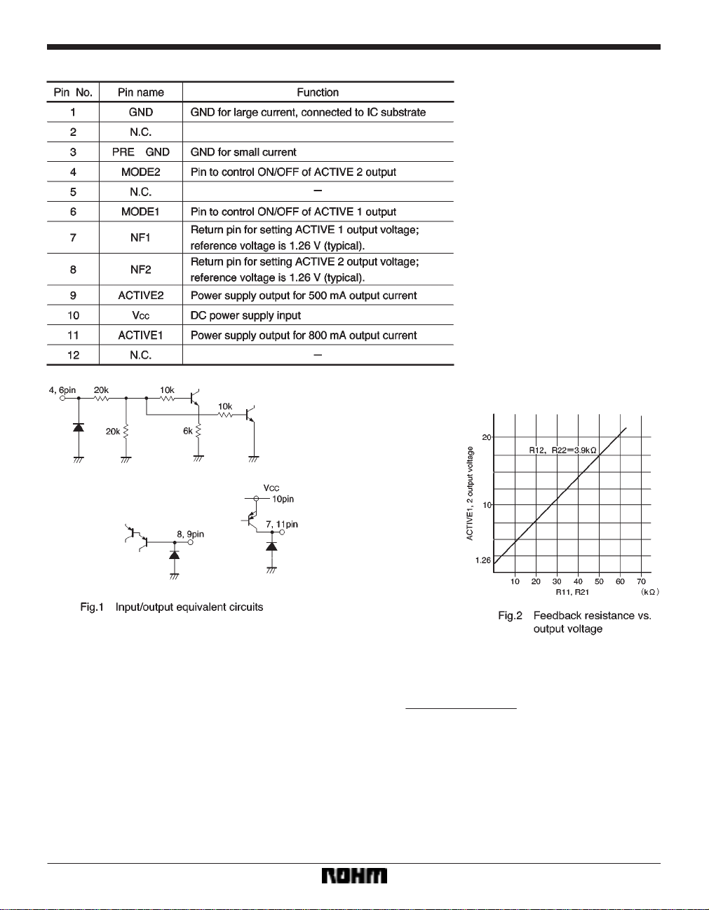
FInput pin descriptions and equivalent circuits
FOutput voltage setting
138
Output voltage setting
R11 (21) R12 (22)
Vref
S
(1.26V)
R12 (22)
Example of output voltage setting resistance
(V
O1 = 6V, VO2 = 8V)
R11 = 15kΩ R21 = 22kΩ
R12 = 3.9kΩ R22 = 3.9kΩ
Page 4
Regulator ICs BA3960
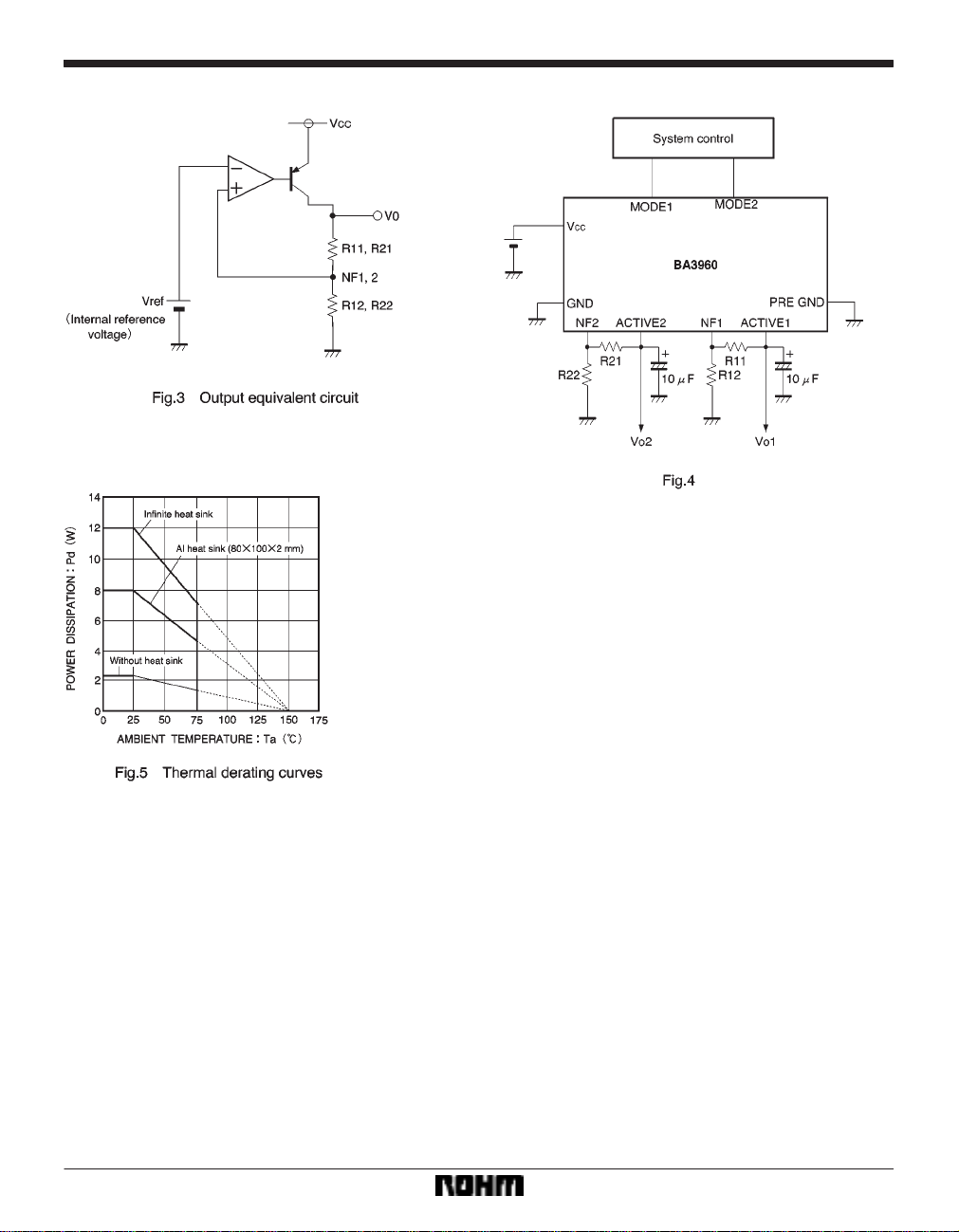
FOutput voltage setting FApplication example
FEstimate of allowable power dissipation
Except under transitional conditions, the power dissipation of this IC is 2.2W per unit at 25_C.
See Fig. 5 for thermal derating characteristics, including
some cases where heat sinks are used.
P
MAX. calculation
S Power consumed by ACTIVE 1 P
S Power consumed by ACTIVE 2 P
S Power consumed internally by each circuit P
MAX. = P1 ) P2 ) P3
P
1 = (VCC * set output voltage) maximum output voltage
2 = (VCC * set output voltage) maximum output voltage
3 = VCC circuit current
139
Page 5
Regulator ICs BA3960
Operation notes
(1) Operating power supply voltage
When operating within proper ranges of power supply
voltage and ambient temperature, most circuit functions
are guaranteed. Although the rated values of electrical
characteristics cannot be absolutely guaranteed, characteristic values do not change drastically within the
proper ranges.
(2) Power dissipation (Pd)
Refer to the heat reduction characteristics (Fig. 5) and
the rough estimation of IC power dissipation presented
on a separate page. If power dissipation exceeds the allowable limit, the functionality of IC will be degraded
(such as reduction of current capacity by increased chip
temperature). Make sure to use the IC within the allowable range of power dissipation with a sufficient margin.
(3) Preventing oscillation at each output
To stop oscillation of output, make sure to connect a capacitor having a capacitance of 10 µF or greater between
GND and each of the Active 1 and 2 output pins. Oscillation can occur if capacitance is susceptible to temperature. We recommend using a tantalum electrolytic capacitor with minimal changes in capacitance. Also, output
can be further stabilized by connecting a bypass capacitor between V
CC and GND.
(4) Overcurrent protection circuit
An overcurrent protection circuit is installed on the Active
1 and 2 outputs, based on the respective current capacity. This prevents IC destruction when the load is shortcircuited, by limiting the current with a curve shape of “7”
in the voltage-current graph. The IC is designed with
margins so that current flow will be restricted and latching
will be prevented even if a large current suddenly flows
through a large capacitor. Note that these protection circuits are only good for preventing damage from sudden
accidents. Make sure your design does not cause the
protection circuit to operate continuously under transitional conditions (for instance, if output is clamped at 1V
or higher, short mode circuit operates at 1VF or lower).
Note that the circuit ability is negatively correlated with
temperature.
(5) Thermal protection circuit
A built-in thermal protection circuit prevents thermal
damage to the IC. All outputs are switched OFF when the
circuit operates, and revert to the original state when
temperature drops to a certain level.
(6) Grounding
To minimize the variation of output voltage due to variations in load current, the GND (pin 1, for large current)
and the PRE GND (pin 3, for small current) pins are separately provided. Make sure to connect circuits to correct
pins.
(7) Output voltage setting
ROHM recommends using a 3.9kΩ resistor for R12 and
R22. Refer to a separate page for the output voltage setting. Note that making a large change to the R12 and R22
values will affect the current capacity.
(8) MODE voltage
Due to the IC’s internal structure, a reverse current flow
will occur if the MODE voltage exceeds the V
Make sure to avoid this.
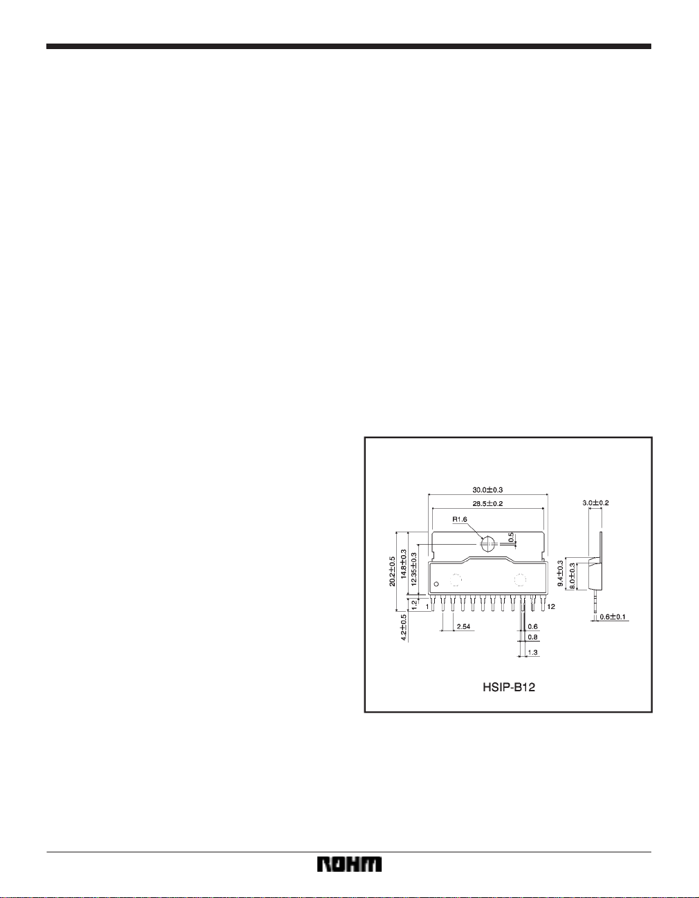
External dimensions (Units: mm)
F
CC voltage.
140
 Loading...