

Standard LDO Regulators
Standard Variable Output
LDO Regulators with Shutdown Switch
BA00DD0WCP-V5,BA00DD0WHFP,
BA00CC0WT,BA00CC0WCP-V5,BA00CC0WFP
●Description
The BA00DD0/CC0 series are low-saturation regulators available for outputs up to 2A/1A. The output voltage can be
arbitrarily configured using the external resistance. These series of LDO regulators are offered in a broad packaging lineup.
This IC has a built-in over-current protection circuit that prevents the destruction of the IC due to output short circuits and a
thermal shutdown circuit that protects the IC from thermal damage due to overloading.
●Features
1) Maximum output current: 2A (BA00DD0 series), 1A(BA00CC0 series)
2) ±1% high-precision output voltage (BA00DD0)
3) Low saturation with PNP output
4) Built-in over-current protection circuit that prevents the destruction of the IC due to output short circuits
5) Built-in thermal shutdown circuit for protecting the IC from thermal damage due to overloading
6) Built-in over- voltage protection circuit that prevents the destruction of the IC due to power supply surges
7) TO220FP andHRP5 packaging (BA00DD0), and TO220FP and TO252 packaging (BA00CC0)
●Applications
Usable in DSP power supplies for DVDs and CDs, FPDs, televisions, personal computers or any other consumer device
●Line up
1A BA00CC0 Series
Part Number Package
BA00CC0WT TO220FP-5
BA00CC0WCP-V5 TO220CP-V5
BA00CC0WFP TO252-5
2A BA00DD0 Series
Part Number Package
BA00DD0WCP-V5 TO220CP-V5
BA00DD0WHFP HRP5
No.11023ECT01
www.rohm.com
© 2011 ROHM Co., Ltd. All rights reserved.
1/9
2011.03 - Rev.C
BA00DD0WCP-V5,BA00DD0WHFP,BA00DD0WT,
BA00CC0WT,BA00CC0WT-V5,BA00CC0WCP-V5,BA00CC0WFP
Technical Note
●ABSOLUTE MAXIMUM RATINGS(Ta=25℃)
Parameter Symbol Limits Unit
Input Power Supply Voltage*1 Vcc -0.3 ~ +35 V
2300(HRP5)
Power Dissipation Pd
mW 1300(TO252-5)
2000(TO220FP-5)
Operating Temperature Range Topr -40 ~ +125 ℃
Ambient Storage Temperature Tstg -55 ~ +150 ℃
Junction Temperature Tjmax +150 ℃
Output Control Terminal Voltage VCTL -0.3 ~ +Vcc V
Voltage Applied to the Tip*3 Vcc peak +50 V
*1 Must not exceed Pd
*2 HRP5 : In cases in which Ta≥25℃ when a 70mm×70mm×1.6mm glass epoxy board is used, the power is reduced by 18.4 mW/℃.
TO252-5 : In cases in which Ta≥25℃ when a 70mm×70mm×1.6mm glass epoxy board is used, the power is reduced by 10.4 mW/℃.
TO252FP-5 : No heat sink. When Ta≥25℃, the power is reduced by 16 mW/℃.
*3 Applied voltage: 200msec or less (tr≥1msec)
50V
tr≧1msec
35V
0V
MAX200msec
(Voltage Supply more than 35V)
●Recommended Operating Range (Ta=25℃)
Parameter Symbol Min. Max. Unit
Input PowerSupply Voltage
Output Current
BA00CC0□□
BA00DD0□□ 3.0 25.0
BA00CC0□□
BA00DD0□□ - 2
Vcc
Io
4.0 25.0
- 1
V
A
Output Control Terminal Voltage VCTL 0 Vcc V
●Electrical Characteristics(ABRIDGED)
BA00CC0□□ Series (unless specified otherwise, Ta=25℃, Vcc=10V, VCTL=5V, Io=500mA, R1=2.2kΩ, R2=6.8kΩ)
Parameter Symbol Min. Typ. Max. Unit Conditions
C-terminal Voltage Vc 1.200 1.225 1.250 V Io=50mA
Circuit Current at the Time of Shutdown Isd - 0 10 µA VCTL=0V
Minimum I/O Voltage Difference ΔVd - 0.3 0.5 V Vcc= 0.95×Vo
Output Current Capacity Io 1.0 - - A
Input Stability Reg.I - 20 100 mV Vcc= 6V→25 V
Load Stability Reg.L - 50 150 mV Io=5mA→1A
Output Voltage Temperature Coefficient* TCVO - ±0.02 - %/℃ Io=5mA ,Tj=0~125℃
*Design guarantee (100% shipping inspection not performed)
BA00DD0□□ Series (unless specified otherwise, Ta=25℃, Vcc=8V, VCTL=3V, Io=500mA, R1=15kΩ, R2=44kΩ)
Parameter Symbol Min. Typ. Max. Unit Conditions
C-terminal Voltage VADJ 1.257 1.270 1.283 V Io=100mA
Circuit Current at the Time of Shutdown Isd - 0 10 µA VCTL=0V
Minimum I/O Voltage Difference ΔVd - 0.45 0.7 V Vcc= 0.95×Vo, Io=2A
Output Current Capacity Io 2.0 - - A
Input Stability Reg.I - 15 35 mV Vcc= 5.7V→25 V, Io=200mA
Load Stability Reg.L - 50 100 mV Io=0mA→2A
Output Voltage Temperature Coefficient* TCVO - ±0.02 - %/℃ Io=5mA ,Tj=0~125℃
*Design guarantee (100% shipping inspection not performed)
www.rohm.com
© 2011 ROHM Co., Ltd. All rights reserved.
2/9
2011.03 - Rev.C
BA00DD0WCP-V5,BA00DD0WHFP,BA00DD0WT,
]
]
]
]
]
]
]
]
BA00CC0WT,BA00CC0WT-V5,BA00CC0WCP-V5,BA00CC0WFP
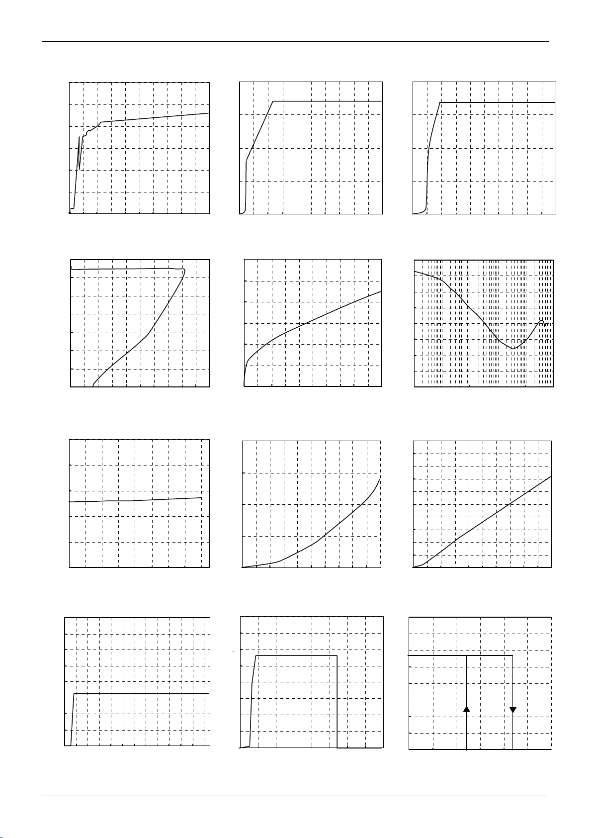
●Reference Data BA00CC0□□(3.3V preset voltage)
(Unless specified otherwise, Vcc=10V, VOUT=3.3V preset, VCTL=3V, Io=0mA, R1=2.2kΩ, and R2=6.8kΩ)
3.0
4.0
4.0
2.5
3.0
2.0
3.0
Technical Note
1.5
1.0
CIRCUIT CURRENT:ICC[mA]
0.5
0.0
02468101214161820
SUPPLY VOLTAGE:VC C[V]
2.0
1.0
OUTPUT VOLTAGE:VOUT[V
0.0
0 2 4 6 8 10 12 14 16 18 20
SUPPLY VOLT AGE:VCC[ V]
2.0
1.0
OUTPUT VOLTAGE:VOUT[V
0.0
0 2 4 6 8 10 12 14 16 18 20
SUPPLY VOLT AGE:VCC[ V]
Fig.3 Input Stability Fig.1 Circuit current Fig.2 Input Stability
3.5
3.0
2.5
2.0
1.5
1.0
OUTPUT VOLTAGE:VOUT[V
0.5
0.0
0 200 400 600 800 1000 1200 1400 1600 1800 2000
OUTPU T C URR ENT:Io[mA]
Fig.4 Load Stability
600
500
Vd[V]
Δ
400
300
200
DROPOUT VOLTAGE:
100
0
0 100 200 300 400 500 600 700 800 900 1000
OUTPUT CURRENT:Io[mA]
Fig.5 Input/Output Voltage Difference
80
70
60
50
40
30
20
RIPPLE REJECTION:R.R[dB
10
0
10 1000 100000
Fig.6 Ripple Rejection Characteristics
Io-ΔVd Characteristics(Vcc=2.95V)
4.5
4.0
3.5
3.0
OUTPUT VOLTAGE:VOUT[V
2.5
2.0
-40 -20 0 20 40 60 80 100 120
AMBIENT TEMPER ATU RE:Ta[℃]
Fig.7 Output Voltage
Temperature Characteristics
8
7
6
5
4
3
2
OUTPUT VOLTAGE:VOUT[V
1
0
0 2 4 6 8 1012141618202224
CONTROL VOLTAGE:VCTL[V]
Fig.10 CTL Voltage vs. Output Voltage
200
150
100
50
CIRCUIT CURRENT:Icc[mA]
0
0 100 200 300 400 500 600 700 800 900 1000
OUTPUT CURRENT:Io[mA]
1000
900
800
700
600
500
400
300
200
CONTROL CURRENT:ICTL[μA]
100
0
0 2 4 6 8 1012 1416 1820
Fig.8 Circuit Current by load Level Fig.9 CTL Voltage vs. CTL Current
(I
4
4
3
3
2
2
1
OUTPUT VOLTAGE:VOUT[V
1
0
0 5 10 15 20 25 30 35 40
OUT=0mA→1A)
SUPPLY VOLT AGE:Vcc[V]
4
4
3
3
2
2
1
OUTPUT VOLTAGE:VOUT[V
1
0
130 140 150 160 170 180 190
Fig.11 Overvoltage Operating
Characteristics (Io=200mA)
www.rohm.com
© 2011 ROHM Co., Ltd. All rights reserved.
3/9
(Io=500mA)
FREQU ENC Y:f[Hz]
100k 10k 1k 100
(Io=100mA)
CON TROL VOLT AGE:VC TL[V]
AMBIEN T TEMPER ATURE:T a[℃]
Fig.12 Thermal Shutdown
Circuit Characteristics
2011.03 - Rev.C
1000k

BA00DD0WCP-V5,BA00DD0WHFP,BA00DD0WT,
]
]
]
]
]
]
]
BA00CC0WT,BA00CC0WT-V5,BA00CC0WCP-V5,BA00CC0WFP
Technical Note
●Reference Data BA00DD0□□(5.0V preset voltage)
(Unless specified otherwise, Vcc=8V, V
6.0
5.5
5.0
4.5
4.0
3.5
3.0
2.5
2.0
1.5
CIRCUIT CURRENT:ICC[mA]
1.0
0.5
0.0
024681012141618202224
SUPPLY VOLTAGE:VC C[V]
8
8
7
7
6
6
5
5
4
4
3
3
2
OUTPUT VOLTAGE:VOUT[V]
2
1
1
0
OUTPUT CURRENT:IOUT[A ]
Fig.16 Load Stability
5.2
5.1
5.0
4.9
OUTPUT VOLTAGE:VOUT[V
4.8
-40 -20 0 20 40 60 80 100
8
7
6
5
4
3
2
OUTPUT VOLTAGE:VOUT[V
1
0
0 2 4 6 8 1012141618202224
AMBIENT TEMPER ATU RE:Ta[℃]
Fig.19 Output Voltage
Temperature Characteristics
CONTROL VOLTAGE:VCTL[V]
Fig.10 CTL Voltage vs. Output Voltage
www.rohm.com
© 2011 ROHM Co., Ltd. All rights reserved.
OUT=5V preset, VCTL=3V, Io=0mA, R1=15kΩ, and R2=44kΩ)
8
7
6
5
4
3
2
OUTPUT VOLTAGE:VOUT[V
1
0
0 2 4 6 8 10 12 14 16 18 20 22 24
SUPPLY VOLT AGE:VCC[V]
8
7
6
5
4
3
2
OUTPUT VOLTAGE:VOUT[V
1
0
0 2 4 6 8 10 12 14 16 18 20 22 24
SUPPLY VOLT AGE:VCC[V]
Fig.15 Input Stability Fig.13 Circuit Current Fig.14 Input Stability
(Io=2A)
800
700
600
500
400
300
200
DROPOUT VOLTAGE:VDRP[V]
100
0
0.5 1.0 1.5 2.0 1.0 2.0 3.0 4.0 4.8
OUTPUT CURRENT:IOUT[A ]
Fig.17 Input/Output Voltage Difference
Iout-ΔVd Characteristics(Vcc=4.75V)
200
180
160
140
120
100
80
60
CIRCUIT CURRENT:[mA]
40
20
0
0.5 1.0 1.5 2.0
OUTPUT CURRENT:IOUT[A]
60
55
50
45
40
35
30
25
20
15
RIPPLE REJECTION:R.R[dB
10
5
0
10 1000 100000
100
FREQU ENC Y:f[Hz]
1k
10k
Fig.18 Ripple Rejection Characteristics
(Iout=100mA)
800
700
600
500
400
300
200
CONTROL CURRENT:ICTL[μA]
100
0
0 2 4 6 8 1012141618202224
CONTROL VOLTAGE:VCTL[V]
Fig.20 Circuit Current by load Level Fig.21 CTL Voltage vs. CTL Current
(I
4
8
4
7
6
3
3
5
4
2
2
3
2
1
OUTPUT VOLTAGE:VOUT[V
1
0
0 5 10 15 20 25 30 35 40
SUPPLY VOLT AGE:Vcc[V]
Fig.11 Overvoltage Operating
Characteristics(Io=200mA)
4/9
OUT=0mA→2A)
8
6
4
2
OUTPUT VOLTAGE:VOUT[V
0
130 140 150 160 170 18 0 190
AMBIEN T TEMPER ATU RE:Ta[℃]
Fig.12 Thermal Shutdown
Circuit Characteristics
2011.03 - Rev.C
100k
1000k

BA00DD0WCP-V5,BA00DD0WHFP,BA00DD0WT,
cc
μ
)
cc
(
BA00CC0WT,BA00CC0WT-V5,BA00CC0WCP-V5,BA00CC0WFP
Technical Note
●Block Diagrams
[BA00CC0WFP]
[BA00DD0WHFP]
V
0.33μF
2
Vref
3
Driver
N.C.(TO252-5)
GND(HRP5)
TOP VIEW
FIN
1 2 3 4 5
TO252-5 HRP5
1 2 3 4 5
OVP
1 5
CTL
TSD
Fin
OCP
GND
Fig.25
PINNo. Symbol Function
1 CTL Output voltage ON/OFF control
2 VCC Power supply voltage input
3 N.C./GND Unconnected terminal/GND*
4 OUT Voltage output
5 C Output voltage regulation terminal
FIN
GND GND
*TO252-5 is N.C., and HRP5 is GND
C(ADJ)
R1
VOUT
4
+
22μF
R2
[BA00CC0WT] [BA00CC0CP-V5] [BA00DD0WCP-V5]
0.33
V
F
Vref
2
Driver
TOP VIEW
TOP VIEW
1 2 3 4 5 1 2 3 4 5
TO220FP-5 TO220FP-5(V5)
OVP
1 5
CTL
TSD
3
GND
OCP
C(ADJ
R1
R2
Fig.26
PINNo. Symbol Function
1 CTL Output voltage ON/OFF control
2 VCC Power supply voltage input
3 GND GND
4 OUT Voltage output
5 ADJ Output voltage regulation terminal
2 3 4 5
1
TO220CP-V5
●Input / Output Equivalent Circuit Diagrams
< BA00CC0WT/BA00CC0WFP >
CTL
25kΩ
25kΩ
10 kΩ
Vcc
VOUT
C
5.5 kΩ
10kΩ
Fig.27
Vcc
Vcc
VOUT
ADJ
500Ω
< BA00DD0WFP >
CTL
Vcc
39kΩ
Ω
2k
31kΩ
Fig.28
●Output Voltage Configuration Method
Please connect resistors R
1 and R2 (which determines the output voltage) as shown in Fig.29.
Please be aware that the offset due to the current that flows from the ADJ terminal becomes large when resistors with large
values are used. The use of resistors with R1=2kΩ to 15 kΩ is recommended.
2
Vo = Vc (V
ADJ) × 1 +
R
1
R
BA□□CC0□□ Vc : 1.225 (Typ.)
BA□□DD0□□
ADJ : 1.270 (Typ.)
V
C
V
OUT
ADJ)
(V
Vc
R2
ADJ
R
)
1
4
VOUT
+
22μF
Fig.29
www.rohm.com
© 2011 ROHM Co., Ltd. All rights reserved.
5/9
2011.03 - Rev.C

BA00DD0WCP-V5,BA00DD0WHFP,BA00DD0WT,
)
)
)
BA00CC0WT,BA00CC0WT-V5,BA00CC0WCP-V5,BA00CC0WFP
Technical Note
●Thermal Design
HRP5 To225FP-5 TO252-5
10
Board size : 70×70×1.6 ㎜3 (board contains a thermal)
Board front copper foil area : 10.5×10.5 ㎜
9
①2-layer board (back surface copper foil area :15×15 ㎜
②2-layer board (back surface copper foil area :70×70 ㎜2)
8
③4-layer board (back surface copper foil area :70×70 ㎜2)
③7.3W
7
6
5
②5.5W
4
Power Dissipation:Pd(W
3
2
①2.3W
1
0
0 25 50 75 100 125 150
Ambient temperature:Ta(℃)
2
2
)
25
(1) When using a maximum heat sick : θj-c=6.25(℃/W)
(2) When us ing an IC alone : θj-c=62.5(℃/W)
20
(1)20.0
15
10
Power Dissipation:Pd(W
5
(2)2.0
0
0 25 50 75 100 125 150
Ambient temperature:Ta(℃)
2.0
Mounted on a Rohm standard board
Board size : 70×70×1.6 ㎜
Copper foil area :7×7 ㎜
TO252-5θja=96.2(℃/W)
1.6
1.30
1.2
0.8
Power Dissipation:Pd(W
0.4
0.0
0 25 5 0 75 100 125 150
Ambie nt te mpe rature :Ta(℃ )
Fig.30 Fig.31 Fig.32
When using at temperatures over Ta=25℃, please refer to the heat reducing characteristics shown in Fig.30 through 32.
The IC characteristics are closely related to the temperature at which the IC is used, so it is necessary to operate the IC at
temperatures less than the maximum junction temperature Tj
MAX.
Fig.31 shows the acceptable loss and heat reducing characteristics of the TO220FP package The portion shown by the
diagonal line is the acceptable loss range that can be used with the IC alone. Even when the ambient temperature Ta is a
normal temperature (25℃), the chip (junction) temperature Tj may be quite high so please operate the IC at temperatures
less than the acceptable loss Pd.
The calculation method for power consumption Pc(W) is as follows :
Pc = (Vcc-Vo)×Io+Vcc×Icca
Vcc:
Input voltage
Vo:
Output voltage
Io:
Load current
Icca:
Circuit current
Acceptable loss Pd≦Pc
Solving this for load current IO in order to operate within the acceptable loss,
Io≦
(Please refer to Figs.8 and 20 for Icca.)
It is then possible to find the maximum load current Io
Pd – Vcc×Icca
Vcc-Vo
MAX with respect to the applied voltage Vcc at the time of thermal design.
Calculation Example
Example 1) When Ta=85℃, Vcc=8.3V, Vo=3.3V, BA33DD0WT
Io≦ With the IC alone : θja=62.5℃/W → -16mW/℃
Io≦200mA (Icca : 2mA) 25℃=2000mW → 85℃=1040mW
1.04-8.3×Icca
5
Please refer to the above information and keep thermal designs within the scope of acceptable loss for all operating
temperature ranges. The power consumption Pc of the IC when there is a short circuit (short between Vo and GND) is :
Pc=Vcc×(Icca+Ishort)
Ishort : Short circuit current
●Terminal Vicinity Settings and Cautions
・Vcc Terminal
Please attach a capacitor (greater than 0.33μF) between the Vcc and GND.
The capacitance values differ depending on the application, so please chose a capacitor with sufficient margin and verify
the operation on an actual board.
・CTL Terminal
The CTL terminal is turned ON at 2.0V and higher and OFF at 0.8V and lower within the operating power supply voltage range.
The power supply and the CTL terminal may be started up and shut down in any order without problems.
www.rohm.com
© 2011 ROHM Co., Ltd. All rights reserved.
6/9
2011.03 - Rev.C

BA00DD0WCP-V5,BA00DD0WHFP,BA00DD0WT,
(
G
G
BA00CC0WT,BA00CC0WT-V5,BA00CC0WCP-V5,BA00CC0WFP
Technical Note
●Vo Terminal
Please attach an anti-oscillation capacitor between VOUT and GND. The capacitance of the capacitor may significantly
change due to factors such as temperature changes, which may cause oscillations. Please use a tantalum capacitor or
aluminum electrolytic capacitor with favorable characteristics and small external series resistance (ESR) even at low
temperatures. The output oscillates regardless of whether the ESR is large or small. Please use the IC within the stable
operating region while referring to the ESR characteristics reference data shown in Figs.33 through 35. In cases where there
are sudden load fluctuations, the a large capacitor is recommended.
EFFECTIVE SERIES RESISTANCE:ESR [Ω]
0.1
100
10
Unstable operating region
Stable operating region
1
Unstable operating region
100
1
10
OUTPUT CURRENT:lo(mA)
1000
OUTPUT CURRENT:lo(mA)
IC
OUT
22μF
C(ADJ)
100
10
1
0.1
0
EFFECTIVE SERIES RESISTANCE:ESR [Ω]
Fig.33:Output equivalent circuit Fig.34:Io vs. ESR characteristics Fig.35: Io vs. ESR characteristics
Unstable operating region
Stable operating region
Unstable operating region
200
400
1000
800
600
(BA□□CC0) (BA□□DD0)
●Other
1) Protection Circuits
Overcurrent Protection Circuit
A built-in overcurrent protection circuit corresponding to the current capacity prevents the destruction of the IC when there
are load shorts. This protection circuit is a “7”-shaped current control circuit that is designed such that the current is
restricted and does not latch even when a large current momentarily flows through the system with a high-capacitance
capacitor. However, while this protection circuit is effective for the prevention of destruction due to unexpected accidents, it
is not suitable for continuous operation or transient use. Please be aware when creating thermal designs that the overcurrent
protection circuit has negative current capacity characteristics with regard to temperature (Refer to Figs.4 and 16).
Thermal Shutdown Circuit (Thermal Protection)
This system has a built-in temperature protection circuit for the purpose of protecting the IC from thermal damage. As
shown above, this must be used within the range of acceptable loss, but if the acceptable loss happens to be continuously
exceeded, the chip temperature Tj increases, causing the temperature protection circuit to operate.
When the thermal shutdown circuit operates, the operation of the circuit is suspended. The circuit resumes operation
immediately after the chip temperature Tj decreases, so the output repeats the ON and OFF states (Please refer to
Figs.12 and 24 for the temperatures at which the temperature protection circuit operates).
There are cases in which the IC is destroyed due to thermal runaway when it is left in the overloaded state. Be sure to
avoid leaving the IC in the overloaded state.
Reverse Current
In order to prevent the destruction of the IC when a reverse current flows through the IC, it is recommended that a diode
be placed between the Vcc and Vo and a pathway be created so that the current can escape (Refer to Fig.36).
2) This IC is bipolar IC that has a P-board (substrate) and P+ isolation layer
between each devise, as shown in Fig.37. A P-N junction is formed between
Reverse current
this P-layer and the N-layer of each device, and the P-N junction operates as a
parasitic diode when the electric potential relationship is GND> Terminal A,
GND> Terminal B, while it operates as a parasitic transistor when the electric
potential relationship is Terminal B GND> Terminal A. Parasitic devices are
Vcc
CTL
OUT
GND
intrinsic to the IC. The operation of parasitic devices induces mutual
interference between circuits, causing malfunctions and eventually the
destruction of the IC itself. It is necessary to be careful not to use the IC in ways
that would cause parasitic elements to operate. For example, applying a
voltage that is lower than the GND (P-board) to the input terminal.
NPN)
B
E
(Pin A)
Resistor
(Pin B)
(Pin B)
Transistor
O
P+
GND
N
P+
N
P
N
P+
P
Parasitic element
GND
N
ig. 37: Example of the basic structure of a bipolar IC
(Pin A)
P+
N
F
Parasitic element
or transistor
N
P
N
P
GND
Fig. 36:Bypass diode
C
B
E
ND
Parasitic element
or transistor
Parasitic element
ND
www.rohm.com
© 2011 ROHM Co., Ltd. All rights reserved.
7/9
2011.03 - Rev.C

BA00DD0WCP-V5,BA00DD0WHFP,BA00DD0WT,
BA00CC0WT,BA00CC0WT-V5,BA00CC0WCP-V5,BA00CC0WFP
●Ordering part number
B A 0 0 C C 0 W H F P - T R
Part No. Output voltage
00:Variable
HRP5
9.395±0.125
(MAX 9.745 include BURR)
8.82 ± 0.1
(6.5)
8.0±0.13 1.017±0.2
1.2575
1.72
0.08±0.05
TO252-5
5.5±0.2 1.5±0.2
6.5±0.2
5.1
123 54
0.5
FIN
+0.2
-
0.1
0.8
TO220CP-V5
10.0
+0.4
0.2
-
15.2
12.0± 0.2
8.0± 0.2
4.92± 0.2
0.82± 0.1
1.0± 0.2
0.92
+0.3
-
0.1
54321
0.73±0.1
0.08 S
C0.5
1.27
φ3.2± 0.1
1.7781.444
(7.49)
2.3±0.2
1.905±0.1
S
0.5±0.1
1.5
0.5±0.1
1.0±0.2
4.5±0.1
+0.2
2.8
-
0.1
0.42± 0.1
(2.85)
4.12
Series
CC0 : 1A
DD0 : 2A
10.54±0.13
0.835±0.2
1.523±0.15
+5.5°
4.5°
−4.5°
+0.1
0.27
−0.05
(Unit : mm)
9.5±0.5
2.5
(Unit : mm)
13.60
16.92
(1.0)
1.58
(Unit : mm)
Shutdown
switch
W : Includes
switch
Package
HFP :HRP5
FP :TO252
CP :TO220CP
T :TO220FP
<Tape and Reel information>
Embossed carrier tapeTape
Quantity
Direction
of feed
2000pcs
TR
The direction is the 1pin of product is at the upper right when you hold
( )
reel on the left hand and you pull out the tape on the right hand
Reel
<Tape and Reel information>
Embossed carrier tapeTape
Quantity
Direction
of feed
2000pcs
E2
The direction is the 1pin of product is at the lower left when you hold
( )
reel on the left hand and you pull out the tape on the right hand
Reel
<Tape and Reel information>
Embossed carrier tapeTape
Quantity
Direction
of feed
500pcs
E2
The direction is the 1pin of product is at the lower left when you hold
()
reel on the left hand and you pull out the tape on the right hand
Reel
1pin
Order quantity needs to be multiple of the minimum quantity.
∗
1pin
Order quantity needs to be multiple of the minimum quantity.
∗
1pin
Order quantity needs to be multiple of the minimum quantity.
∗
Technical Note
Packaging and forming specification
TR: Embossed tape and reel
(HRP5)
E2: Embossed tape and reel
(TO252-5,TO220CP)
None : Container Tube
V5 :Foaming(V5 only)
Direction of feed
Direction of feed
Direction of feed
www.rohm.com
© 2011 ROHM Co., Ltd. All rights reserved.
8/9
2011.03 - Rev.C

BA00DD0WCP-V5,BA00DD0WHFP,BA00DD0WT,
BA00CC0WT,BA00CC0WT-V5,BA00CC0WCP-V5,BA00CC0WFP
TO220FP-5
−0.2
+0.4
17.0
13.5Min.
+0.3
10.0
−0.1
+0.3
7.0
1.8±0.28.0±0.2
12.0±0.2
0.7
−0.1
φ
3.2±0.1
1.2
0.8
+0.3
4.5
−0.1
+0.2
2.8
−0.1
<Tape and Reel information>
Quantity
Direction of feed
TubeContainer
500pcs
Direction of products is fixed in a container tube
Technical Note
1.778
23451
0.5±0.1
2.85
(Unit : mm)
Order quantity needs to be multiple of the minimum quantity.
∗
www.rohm.com
© 2011 ROHM Co., Ltd. All rights reserved.
9/9
2011.03 - Rev.C

Notes
No copying or reproduction of this document, in part or in whole, is permitted without the
consent of ROHM Co.,Ltd.
The content specied herein is subject to change for improvement without notice.
The content specied herein is for the purpose of introducing ROHM's products (hereinafter
"Products"). If you wish to use any such Product, please be sure to refer to the specications,
which can be obtained from ROHM upon request.
Examples of application circuits, circuit constants and any other information contained herein
illustrate the standard usage and operations of the Products. The peripheral conditions must
be taken into account when designing circuits for mass production.
Great care was taken in ensuring the accuracy of the information specied in this document.
However, should you incur any damage arising from any inaccuracy or misprint of such
information, ROHM shall bear no responsibility for such damage.
The technical information specied herein is intended only to show the typical functions of and
examples of application circuits for the Products. ROHM does not grant you, explicitly or
implicitly, any license to use or exercise intellectual property or other rights held by ROHM and
other parties. ROHM shall bear no responsibility whatsoever for any dispute arising from the
use of such technical information.
The Products specied in this document are intended to be used with general-use electronic
equipment or devices (such as audio visual equipment, ofce-automation equipment, communication devices, electronic appliances and amusement devices).
The Products specied in this document are not designed to be radiation tolerant.
While ROHM always makes efforts to enhance the quality and reliability of its Products, a
Product may fail or malfunction for a variety of reasons.
Please be sure to implement in your equipment using the Products safety measures to guard
against the possibility of physical injury, re or any other damage caused in the event of the
failure of any Product, such as derating, redundancy, re control and fail-safe designs. ROHM
shall bear no responsibility whatsoever for your use of any Product outside of the prescribed
scope or not in accordance with the instruction manual.
The Products are not designed or manufactured to be used with any equipment, device or
system which requires an extremely high level of reliability the failure or malfunction of which
may result in a direct threat to human life or create a risk of human injury (such as a medical
instrument, transportation equipment, aerospace machinery, nuclear-reactor controller, fuelcontroller or other safety device). ROHM shall bear no responsibility in any way for use of any
of the Products for the above special purposes. If a Product is intended to be used for any
such special purpose, please contact a ROHM sales representative before purchasing.
If you intend to export or ship overseas any Product or technology specied herein that may
be controlled under the Foreign Exchange and the Foreign Trade Law, you will be required to
obtain a license or permit under the Law.
Notice
www.rohm.com
© 2011 ROHM Co., Ltd. All rights reserved.
Thank you for your accessing to ROHM product informations.
More detail product informations and catalogs are available, please contact us.
ROHM Customer Support System
http://www.rohm.com/contact/
R1120
A
 Loading...