ROHM 2SK3065 Datasheet

Transistors
Small switching (60V, 2A)
2SK3065
2SK3065
Features
!
1) Low on resistance.
2) High-speed switching.
3) Optimum for a pocket resource etc. because of
undervoltage actuation (2.5V actuation).
4) Driving circuit is easy.
5) Easy to use parallel.
6) It is strong to an electrostatic discharge.
Structure
!
Silicon N-channel
MOS FET transistor
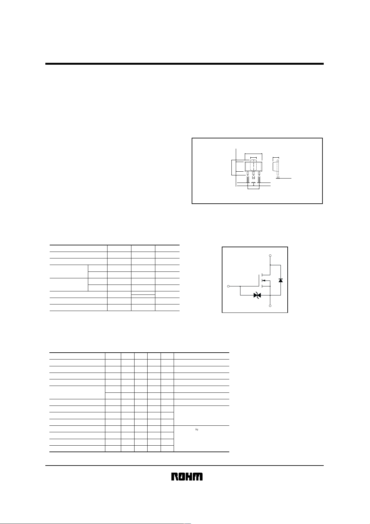
Absolute maximum ratings
!
Parameter
Drain-source voltage
Gate-source voltage
Drain current
Reverse drain
current
Total power dissipation(Tc=25°C)
Channel temperature
Storage temperature
∗1 Pw ≤ 10µs, Duty cycle ≤ 1%
∗2 When mounted on a 40 × 40 × 0.7 mm alumina board.
Continuous
Pulsed
Continuous
Pulsed
(Ta = 25°C)
Symbol Limits Unit
1
∗
1
60 V
±20
2I
2
8
0.5
∗
2
2
150
DSS
V
V
GSS
D
∗
I
DP
I
DR
I
DRP
P
D
Tch
Tstg °C−55∼+150
External dimensions
!
ROHM
EIAJ : SC-62
: MPT3
Internal equivalent circuit
!
(Units : mm)
0.5±0.1
−0.1
+0.2
+0.5
−0.3
2.5
4.0
0.4±0.1
1.5±0.1
1.0±0.3
Abbreviated symbol : KE
4.5
1.6±0.1
0.5±0.1
3.0±0.2
+0.2
−0.1
1.5±0.1
(3)(2)(1)
0.4±0.1
1.5±0.1
Drain
+0.1
0.4
−0.05
(1) Gate
(2) Drain
(3) Source
V
A
A8
A
Gate
A
W
°C
∗ A protection diode has been built in between the
gate and the source to protect against static
electricity when the product is in use.
Use the protection circuit when rated voltages are
exceeded.
∗Gate
Protection
Diode
Source
Electrical characteristics
!
Parameter
Gate-source leakage
Drain-source breakdown voltage
Zero gate voltage drain current
Gate threshold voltage
Static drain-source on-state
resistance
Forward transfer admittance
Input capacitance
Output capacitance
Reverse transfer capacitance
Turn-on delay time
Rise time
Turn-off delay time
Fall time
Pw ≤ 300µs, Duty cycle ≤ 1%
∗
(Ta = 25°C)
Symbol
GSS
I
V
(BR)DSS
I
DSS
V
GS(th)
R
DS(on)
R
DS(on)
Yfs
∗
C
iss
C
oss
C
rss
t
d(on)
t
r
t
d(off)
t
f
Min.
−
60
−
0.8
−
−
1.5
−
−
−
−
−
−
−
Typ.
Max.
±10
−
−−
−
10
−
1.5
0.25
0.32
0.45 I
0.35
−
−
−
160
85
−
25
−
20
−
50
−
120
−
70
−
Unit
µA
µA
Ω
Ω
S
pF
pF
pF
ns
ns
ns
ns
V
V
GS
= ±20V, V
V
D
= 1mA, V
I
V
DS
= 60V, V
V
DS
= 10V, ID = 1mA
I
D
= 1A, V
D
= 1A, V
I
D
= 1A, V
V
DS
= 10V
V
GS
= 0V
= 1MHz
f
I
D
= 1A, V
V
GS
= 4V
R
L
= 30Ω
R
G
= 10Ω
Test Conditions
DS
= 0V
GS
= 0V
GS
= 0V
GS
= 4V
GS
= 2.5V
DS
= 10V
DD
30V

Transistors
Packaging specifications
!
2SK3065
Package
Code
Type
Basic ordering unit
(pieces)
2SK3065
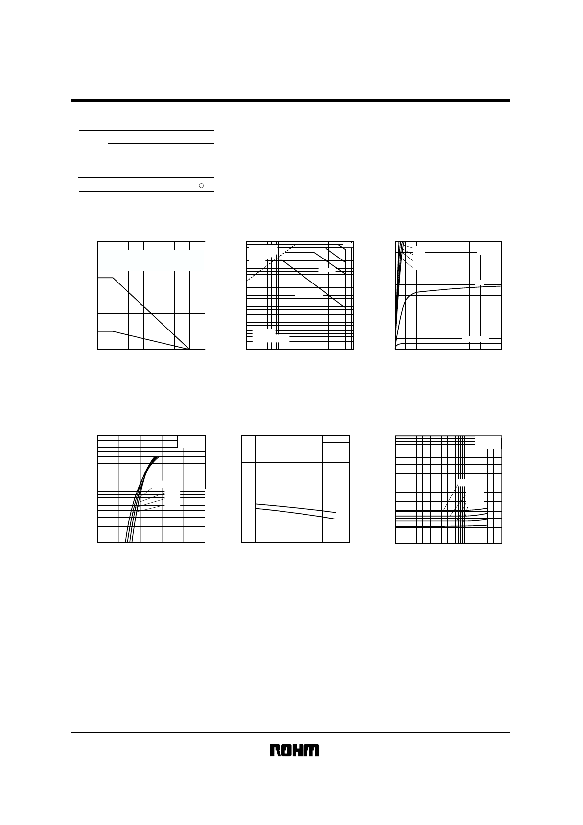
Electrical characteristic curves
!
3
(W)
D
When mounted on a 40 x 40 x 0.7 mm
aluminum-ceramic board.
2
1
TOTAL POWER DISSIPATION : P
0
0 25 50 75 100 125 150 175
AMBIENT TEMPERATURE : Ta(°C)
Fig.1 Total Power Dissipation vs.
Case Temperature
Taping
T100
1000
10
Operating in this
area is limited by
DS(on)
R
1
(A)
D
0.1
0.01
DRAIN CURRENT : I
Ta=25°C
Single Pulsed
0.001
0.1 1 10 100
DRAIN-SOURCE VOLTAGE : VDS(V)
Pw=10ms
DC OPERATION
Fig.2 Maximum Safe Operating Area
100µs
1ms
2
4V
3.5V
3V
2.5V
1
DRAIN CURRENT : ID(A)
0
0510
DRAIN-SOURCE VOLTAGE : VDS(V)
2V
VGS=1.5V
Ta=25°C
Pulsed
Fig.3 Typical Output Characteristics
10
(A)
D
1
DRAIN CURRENT : I
0.1
054
GATE THRESHOLD VOLTAGE : VGS(th)(V)
Ta=−25°C
25°C
75°C
125°C
321
VDS=10V
Pulsed
Fig.4 Typical Transfer Characteristics
4
(th)(V)
GS
3
2
1
GATE THRESHOLD VOLTAGE : V
0
−50 150100
−25
CHANNEL TEMPERATURE : Tch(°C)
Fig.5 Gate Threshold Voltage vs.
Channel Temperature
10mA
ID=1mA
50250
VDS=10V
75
125
10
Ω)
(on)(
DS
1
STATIC DRAIN-SOURCE
ON-STATE RESISTANCE : R
0.1
0.01 10
Fig.6 Static Drain-Source On-
0.1
DRAIN CURRENT : I
State Resistance vs.
Drain Current(Ι
Ta=125°C
−25°C
1
)
75°C
25°C
D
(
A)
V
GS
Pulsed
=4V
 Loading...