

Roadstar CTV-1450 Service Manual

R
- CTV-1450_2050
- CTV-1450_2050
CTV-1450_2050
Service Manual
Service Manual

SpeakerBLOCK DIAGRAM
Key
Tuner
IR
Audio Processor
TDA 9859
Memory
AT24C16
Micro Processor (UOC IC )
TDA 9351
FRONT
Audio Output
AN17821
SWITCH IC
HEF4052BP
Video Amplifier
SCART
CRT
SMPS
AV
110VDC
28V
13V
8V
5V
Horizontal
O/P driver
Vertical output
STV 9302A
Horizontal
O/P TR.
FBT

T
Ricerca & Innovazione
Elenco dei Materiali (B.o.M.)
TV 14" - Roadstar
modello:
pagina: 1 / 2
data: 09-nov-2005
revisione: 08
1450KT
n.° livello
1 1
2 2 2) Assieme cabinet frontale 1 n.°
3 3 3) cabinet frontale verniciato con scritte 1 n.°
4 4 4) cabinet frontale non verniciato 1 n.°
5 5 5) plastica grezza 825,00 g
6 4 4) vernice 62,70 g
7 4 4) inchiostro per scritte 0,03
8 4 4) staffa fissaggio cabinet destra 1 n.°
9 4 4) staffa fissaggio cabinet sinistra 1 n.°
10 4 4) collante per staffe 0,020 g
11 5 5) graniglia per collante 0,002 g FA/LOC
12 5 5) solvente 0,018 g
13 3 3) pulsante accensione verniciato 1 n.°
14 4
15 5 5) plastica grezza x g
16 4 4) vernice x g
17 3 3) molla pulsante accensione 1 n.°
18 3 3) pulsantiera verniciata (5 p.) 1 n.°
19 4 4) pulsantiera non verniciata 1 n.°
20 5
21 4 4) vernice x g
22 3 3) vite per fissaggio pulsantiera, 4x12BT 2 n.°
23 3 3) logo ROADSTAR CTV 1450-K
24 3 3) coperchio ricevitore IR 1 n.°
25 3 3) lente per led e ricevitore IR 1 n.°
26 3 3) rondella cinescopio in gomma, 6x22x3mm 4 n.°
27 3 3) colla per rondelle 0,5 g
28 3 3) cinescopio 14", generico, yammato 1
29 3 3) vite per fissaggio cinescopio, 5x20 tipo B 4 n.°
30 3 3) cavo di massa per cinescopio 1 n.° SKD
31 3 3) molla con gancio per tensione cavo di massa 1 n.°
32 3 3) bobina di smagnetizzazione 1 n.°
33 3 3) fascetta in plastica, 2.5x100 mm, bianca 4 n.°
34 3 3) sostegni per bobina smagnet.- filo gommato 4
35 3 3) cablaggio giogo, 400 mm 1
36 3 3) staffa altoparlante sinistro 1 n.°
37 3 3) altoparlante, 16Ω, 3W, Φ 90mm 1 n.°
38 3 3) guarnizione altoparlante 1 n.° FA
39 3 3) connettore altoparlante 1 n.°
1) Assieme televisore finito 1 n.°
descrizione componenti
4) pulsante accensione non verniciato
5) plastica grezza
quant.
x TV
1 n.°
xg
1 n.°
un. di
misura
g LOCAL
FA/LOC
FA/LOC
FA/LOC
FA/LOC
FA/LOC
n.° vedi tab.
FA/LOC
FA/LOC
n.° SKD
n.° SKD
prov.
LOCAL 1600005000
LOCAL
LOCAL
LOCAL
FA
FA
LOCAL 1600006000
FA
LOCAL
LOCAL
FA
LOCAL
FA
LOCAL
LOCAL
FA
FA
FA
LOCAL
SKD
FA
SKD
SKD
n.°
disegno
vedi tabella p. 2 vedi tabella
JE1----B012-A 1100001506
ES14AMP01 1500005001
MG3X0020---G7 1100001860
MB5X0005---E3 1600002000
JS4401-A001-P 1100001480
JW2321-C001-A 1600004000
codice
componente
1200004770
1200004919
1500001000
1500002000
1500003000
1200001752
1200001751
1600008000
1600008001
1600008002
1200002010
1500001000
1500002000
1100001810
1600007000
1200004935
1500001000
1500002000
1100001767
1100009120
1200001478
1200001725
1100001920
1400000138
1100001753
1100009192
1200001403
1100008482
1100003355

40 3 3) vite per fissaggio altoparlante, 4x12BT 2 n.° FA/LOC
41 3 3) nastro in feltro 25mm per bordo altoparlante 0,04 m FA/LOC
42 3 3) cravatta ferma cavo in metallo, 57 mm 1
43 3 3) assieme chassis 14" 1
n.°
FA/LOC
n.° SKD
44 3 3) cappuccio per pulsante accensione 1 n.° FA
45 3 3) cavo di alimentazione 220 V 1
n.° SKD
46 3 3) filo gommato nero per cavo alim., 100 mm 1 n.° FA
47 3 3) ferma cavo per cavo alimentazione 1 n.° FA
48 3 3) distanziatore cavo ventosa HV 2 n.° FA
49 3 3) fascetta in plastica, 2.5x100 mm, bianca 4 n.°
FA/LOC
1100001767
1100001853
1100001858
vedi tabella p. 2 vedi tabella
1200000687
JP2202-V004-X 1100009704
1100001861
1200000758
MG3X0040---G2 1100003293
1100001860

Ricerca & Innovazione
Elenco dei Materiali (B.o.M.)
TV 14" - Roadstar
modello:
pagina: 2 / 2
data: 09-nov-2005
revisione: 08
1450KT
n.° livello
50 2 2) Assieme cabinet posteriore 1 n.°
51 3 3) cabinet posteriore non verniciato 1 n.°
52 4 4) plastica grezza 1.181,0 g
53 3 3) nastro in feltro 25mm 0,6 m
54 3 3) etichetta articolo e codice a barre 80x65mm 1 n.°
55 3 3) vite per assiemaggio cabinet, 4x16BT 4 n.°
56 Busta accessori 1 n.°
57 3 3) libretto istruzioni 1 n.°
58 3 3) scheda di garanzia Roadstar 1 n.°
59 3 3) schema circuito elettrico CTV 1450KT, VE02 1
60 3 3) lista Centri Assistenza Tecnica 1
61 3 3) etichetta PVC per schermo (POP) 1
62 3 3) telecomando 1 n.°
63 3 3) batterie per telecomando 1,5 V, UM3, AA 2 n.°
64 3 3) busta polietilene 235x330 mm 1 n.°
65 1
66 3 3) scatola imballo piana 1 n.°
67 3 3) busta TV polietilene, 850x800 mm 1 n.°
68 3 3) polistirolo per imballo inferiore (dx e sx) 1 n.°
69 3 3) polistirolo per imballo superiore (dx e sx) 1 n.°
70 3 3) etichetta articolo e codice a barre, 57x18 mm 3 n.°
71 3 3) nastro adesivo trasparente 72 mm 4,5 m
72 Materiali di supporto alla lavorazione
73 3 3) nastro in carta 12 mm 0,1
74 3 3) cartellino di lavorazione "history card" 1
75 3 3) stagno per saldature 2
1) Scatola imballo TV 1 n.°
descrizione componenti
quant.
x TV
un. di
misura
n.° LOCAL
n.° LOCAL
n.° LOCAL
n.° FA/LOC
LOCAL
LOCAL
FA/LOC
LOCAL
FA/LOC
LOCAL
LOCAL
SKD
SKD
LOCAL
LOCAL
LOCAL
LOCAL
LOCAL
FA
FA/LOC
m FA/LOC
g FA/LOC
n.°
disegno
BT-0369A---CB 1100009207
MT0X0008---T3 1100002593
codice
componente
1200004764
1200004800
1600001001
1100001853
1500008001
1100004229
1100009248
1100010179
1100010167
1100010185
1100009659
1300000385
1300001358
1300000388
1300000720 B
1300000720 T
1100001815
1300000769
1400000151
1100001770
1400000301
n.° livello
1 1
2 2 2) televisore imballato 20
3 2 2) film polietilene estensibile 30 m
Legenda provenienza: FA = India; SKD = Cina; LOCAL = locale; FA/LOC = India o locale
1) Assieme imballo
descrizione componenti imballo
quant.
x imb.
un. di
misura
n.°
prov.
LOCAL
n.° disegno /
specifica
codice
componente
1600009001

Tipo Cinescopi
o
A
X
A
A
R
n°. Provenienza Codice compon.
Provenienza Codice componente Tipo Chassis
1 SKD 1200004804
2 SKD 1700002003
3 SKD 1700002004
34LEX10
SAMTEL - India 1100001679 VE02 14SMT
34KQW42X01 SAMSUNG SDI - Malaysia 1700001001 VE02 14SMG
33EKC..X.. EKRANAS - Lithuania 1700001002 VE02 14EK
4
5

VILEUR UOC STEREO SCH
C710
0.1u
47u/16V
C202 0.01u
+
LM-01
C112
100u16V
C116
0.068u
C117
0.15u
C118
6800p
R112
12K
R113
100
+
C812
R815
5.6K
1
2
XS152
1
2
3
XS151
1
2
3
4
5
XS156
TDA9859
AV1 L
1
2 31
3
MAIN L
+
CSMO
4
MAIN R
5
6
VCC
AUDIO
7
OUT R
8
GND
VO2
9
VI8
10
11
CBR1
12
CBR2
WOOF
13
OUT R
14
CTR
MAIN
15
OUT R
16
SCL
R814
5.6K
N151
AN17821
Vcc
2
3
1
10u/16V
C152
+13V
0.01u
+
C151
R191
2.2K
C191
10u/16V
1u
VD702
1N4148
C334
2200u/25V
R192
8.2K
+
+
C153
1u
VD141
100u/16V
1N4148
R141
V141
10K
2SA1015
R142
10K
V142
2SC1815
R340
100
R338
+
330
10u/16V
R157
C141
270K
+
+8V
R143
22K
R404
1.5K
INV IN
1
C412
0.033u
R412
1.5K
R731
3.3K
+8V
R734
10K
+
C335
R339
110
+3.3V
+5V
N701
AT24C16
C703
XP2001
0.01u
8
+
R701 3.3K
R710 3.3K
R712 3.3K
C702
7
47u/16V
R709
SCL
6
100
R711
5
SDA
100
+3.3V
R724
10K
1.2K
2K
2.7K
12K
R733 3.3K
R723
47
R722
3.9K
12 Vss A
13
C301
0.22u
C303
C307
C309
2.2u
L301
+8V
+ +
1u
0.01u
10uH
R301 15K
2200p
4700p
R401 100
R402 100
C302
47u/16V
C304
0.22u
C305
C306
C308
C401
1000p
C402
1000p
14
+
15
16
17
18
19
0.1u
20
+
C310
4.7u
21
22
23
TO XP2001
SW705
SW704
SW703
SW702
SW701
P+
P-
V+
V-
MENU
1
2
XS701
FROM XS701
1 2
1
2
3
4
R729
R728
R727
R726
24
R403
25
39K
C403
26
0.1u
27
C207
0.022u
28
C311
3300p
29
+ +
C312
+ + +
2200u/25V
R632
R633
VR631
+26V
R634
2.4K
+13V
C647
C652
2200u/25V
C667
1000u/16V
TP91
51K
51K
B+ ADJ
20K
VD632
1N4148 VD652
C633
0.033u
10u/16V
4700p
30
C314
C313
31
820p
C315
4.7u
R302
2.7K
R633A
1.5K
R652
220
B+ +110V
R635
1K
R636
K
10K
R
A
V631
TL431LP
FROM XS231
+9V
R227
220
R223
C223
4.7K
R740 220
1000/1KV
TVR4J
TVR4J
!
!
N611
KA5Q0765
C617
33u
0.01u
C221
1000p
1
22
VD201
R201
MTZJ5C1
3.3K
R202
R204
270
47K
R203
C603
C605
L602
1000/1KV
LF-033
VD605
TVR4J
VD606
TVR4J
VD611
TVR4J
VD616
5V1HSC
R611
68K
R612
68K
C618
C619
0.1u
0.033u
4
5
3
+
R617
VD619
2.4K
HZ9A3
NAME
VALUE
IF
BT+31V
C201
+
BP+5V
C206
3.3u
L911
XS602
2
!
XS601XP601
1
!
2
SDA
SCL
AGC
1
AS
P10X180M
!
t
PS601
SW601
A04
!
T3.15AL/AC 250V
L611
LF-05
C615
1000/1KV
680p/2KV
TPAGC
R602 1.8
L601
LF-033
C601
0.22u/AC275V
1
C616
R737 220
C607A
470p/AC 400V
!
R601
220K
F601
R221
1.5k
VD603
5
VD604
!
2
R226
220
L221
0.75uH
V221
2SC1674C
R224
1.2K
+8V
!
+
C611
C610
2200p/1KV
220u/400V
PC817B/C
R229
33
N612
VD613
RGP10J
VD615
1N4148
C706
10u/50V
C225
0.01u
+
2
1
4
3
VD614
RGP10J
R616
3.3K
C614
470p
R615
2.2
K2955
R718
8.5K
N702
KA33
!!
1
3
7
8 11
! !
!
C620
1000p/AC400V
Z221
5
4
3
2
1
+B
1/2W 0.47
1/2W 0.47
1/2W 0.47
470p/2KV
R641
1/2W 0.47
!
R646
R651
R666
!
C631
!
VD631
RGP10J
!
VD641
RGP10D
!
!
470p/1KV
470p/1KV
C651
C632
220u/160V
!
+
C646
!
VD646
RGP15D
!
VD651
RGP10D
C666 470p/1KV
!
VD666
RGP15D
+
C641
470p/1KV
C642
100u/35V
T611
0087
16
10
15
14
12
13
R619
24M
N301
TDA9361
1
STAND BY
SCL
3
SDA
TUNING
4
NTSC SW
5
/AC TEST
KEY
6
XTAL OUT
7 VOL1 XTAL IN
8
MUTE
Vss C/P
9
10
BAND1
11
BAND2
OSCGND
SECPLL
Vp2
DECDIG
BLANKING
PHL2LF
PHL1LF
GND3
DECBG
AVL
/EWD
VDRB
VDRA
IF1
B2/UIN
G2/YIN
R2/VIN
INSSW2
AUDOUT
/AMOUT
CHROMA
CVBS/Y
IF2
IREF
CVBSINT
VSC
TUNER AGC
AUDEEM
/SIF1
DECSDEM
/SIF2
GND2
SNDPLL
/SIF AGC
PLL IF
AUDEXT
/QSSO
AVL/REFO32
VD402
MTZJ8C2
V666
2SB1443
R667
10K
N656
KA7805
1
2
C656
R668
R708
1.2K
330
2SC1815
470u/16V
R707
V703
1K
2SC1815
VD701
C701
V701
0.01u
R653
VD667
1N4148
1N4148
12K
VddP
RESET
VddC
VddA
BOUT
GOUT
ROUT
BCLIN
IFVO
/SVO
EHTO
FBISO
H OUT
R706
22K
IRIN
VpE
GND1
AV22
AV1
Vp1
3
+
R742
64
63
62
61
60
59
58
57
56
55
54
53
52
51
50
49
48
47
46
45
44
43
42
41
40
39
38
37
36
35
34
33
L402 1uH
L401 1uH
VD401
MTZJ8C2
1
R705
330
R702
10K
R741
3.3K
3.3K
R743
100
C719
0.01u
X701
12M
C716
C717
33p
33p
C715
C714
0.01u
10u/16V
+
C713
0.01u
+
R373
330
R372
330
R371
330
R361
10K
+
C353
C574
0.022u
10u/16V
C352
0.022u
C351
0.022u
C317
+
R304
1K
10u/16V
C336
0.1u
C332
0.01u
C331
+
100u/16V
C316
R303
390
0.1u
C551
1000p
R563
27K
N671
KA7808
2
3
R671
+8V
2
56
+
C671
470u/16V
R661
33
VD661
HZ3C2
+5V
R704
1K
R703
V702
22K
2SC1815
STANDBY
H:ON L:OFF
N703
0038A2
L703
10uH
+3.3V
+
C718
2.2u
L702
10uH
+3.3V
+3.3V
L701
10uH
C712
10u/16V
+8V
R362
R363
22K
L331
10uH
R331
R556
+
L333
10uH
1.8K R334
R555
100K
27K
R501
2.2K
VD561
MTZJ8C2
+3.3V
C661
100u/16V
33K
V331
2SC1815
R333
220
+5V
C361
560p
+8V
C333
47u/16V
+
V332
Z331
XT5.5M
Z332
XT6.5M
Z333
XT6.0M
2SC1815
L332
8.2uH
100
STAND-BY
4
6
5
C160
+
R156
68K
MAIN PCB
LA78040
VCC
PUMP UP
2
3
C411
180p
VD411
RGP10D
VD412
MTZJ18
+15V
CH1in
6800p
N411
VEE
4
-15V
CH1out(-)
GND(CH1out)
CH1out(+)
GND
7
6800p
C155
C414
100u/35V
VOLUME
GND(CH2out)
CH2 OUT(-)
CH2 IN
9
8
C156
+
1u
C157
R155
1.8K
C154
+
1u
R153
1.8K
VCC2
V OUT
NON-INV IN
6
5
7
+
R411
C415
1
0.22u
CH2 OUT(+)
10
12
11
R117
C111
100
0.47u
+
C113
0.47u
R118
+
100
L111
+8V
+
10uH
C115
C114
0.01u
47u/16V
R111
12K
47u/16V
R414
100
2
!
C416
0.1u/100V
L411
22uH
R413
1
1
!
N111
V811
2SC1815
SP101
470u/25V
470u/25V
R504
C502
VD941
GND
XS903
1
2
IK
R911
47
B
3
R921
G
4
47
R
5
R931
GND
47
6
R932
10K
N101
BU4052
1
2
3
4
5
6
7
8
270
16
Y0B
VDD
15
Y2A
Y2B
14
ZB
Y1A
13
ZA
Y3B
12
Y0A
Y1B
Y3A
11
INH
A0
10
VEE
9
VSS
A1
C514
4.7u/160V
+
R512
10K
VD511
BAV21
R513
+180V
C542
10u/250V
R531
1W 1
+
C532
R536
1W 1
C536
+
2
T501
+
C503
47u/35V
SP102
TO XP2102
GND
1
IK
2
3
B
4
G
5
R
6
GND
XS371
32
AV1 R
P2P1
30
AV2 R
C126
CPS1
29
0.015u
28
AV2 L
C125
27
CPS2
0.015u
AUDIO
26
OUT L
25
GND
VO1
24
VI7
23
C123
0.068u
CBL1
CBL2
WOOF
OUT L
CTL
MAIN
OUT L
SDA
R812
33
R813
150
R116
22
12K
C122
21
0.15u
20
C121
6800p
19
R115
18
12K
17
R114
100
+8V
R562
100
R561
1
10K
C561
100p/500V
+15V
-15V
+26V
R503
R502
100
2SC2383
1K
V501
1000p/500V
C501
3900p/500V
R915
2
10K
MTZJ8.2
R912
10K
R925
2
10K
2SC2330
R923
300
VD921
1N4148
R935
2
10K
V931
2SC2330
R933
300
VD931
R922
10K
1N4148
L101
+8V
10uH
+
C101
47u/16V
R102
10K
R103
10K
1
!
C513
2.7
0.36u/200V
VD541
LF-05
VD536
RGP10D
L511
GRP10J
470p/500V
VD531
RGP10D
!
470p/500V
V511
!
2SD1651C
L512
LF-05
+
!
!
V911
2SC2330
R913
300
VD911
1N4148
V921
C541
C531
V912
BF420
V913
C911
BF421
220
R914
47
V922
BF420
V923
BF421
C921
R926
220
330
R924
47
V932
BF421
V933
BF420
C931
R936
220
330
R934
47
R553
680
!
C511
C512
680p/2KV
9100p/1.6KV
R916
330
VD854
MTZJ8C2
VD552
1N4148
R511 1K
R917
220
R927
220
R937
220
VD846
MTZJ5C1
VD831
MTZJ5C1
VD841
MTZJ5C1
VD821
MTZJ5C1
C853
470p
C852
470p
C851
470p
VD871
MTZJ8C2
470u/16V
VD801
MTZJ8C2
VD836
MTZJ5C1
VD551
MTZJ22D
R552
1K
L513
016
1
!
7
6
5
3
4
1
10
3
R514
5
3.9
+
C515
10u/160V
CRT°å
L911
R918
1.5K
R928
1.5K
R938
1.5K
L913
82uH
1
J
R951
XS902
GND
HEATER
CRT GND
C847
C832
C842
C822
C811
47u/16V
R554
560K
T511
0083
+
1u
C846
470p
+
1u
C831
470p
+
1u
C841
470p
+
1u
C821
470p
MTZJ8C2
MTZJ8C2
+
+
VD806
MTZJ8C2
VD826
MTZJ5C1
+110V
VD853
VD852
MTZJ8C2
VD851
C802
C801
470p
!
R846
1K
R847
100K
R831
3.9K
R832
10K
R841
1K
R842
100K
R821
3.9K
R822
10K
R853
75
R852
75
R851
75
R871
5.6K
C861
1000p
R811
68
R801
100
C807
+
47u/16V
C806
470P
C827
+
1u
C826
470p
C837
+
1u
C836
470p
HV
FO
SC
8
10u/16V
1K
R571
C571
0.1u
VD572
1N4148
VD573
1N4148
R572
B OUT
82uH
L912
G OUT
82uH
R OUT
XS905
SOCKET
!
R955
2.2M
1
R941
5.6
200V
R854
75
R806
100
R826
3.9K
R827
10K
R836
3.9K
R837
10K
R575
1.8K
+
C573
10K
C572
0.47u
+
C955
+
10u/250V
C941
10u/250V
XS801
ARo
1
ARi1
ALo
3
A GND
B GND
5
ALi1
B IN/OUT
7
SW
G GND
9
G IN
11
R GND
13
BL GND
R IN
15
BLANK IN
Vo GND
17
Vi GND
Vo
19
Vi/Y
SHIELD
21
XS807
1
2
3
4
5
6
7
8
4
3
2
1
1
2
3
4
+180V
5
XS551
VD571
MTZJ8C2
+8V
R573
4.7K
A51JSY61X03
2
4
6
8
10
12
14
16
18
20
XS511
DY
VE901
RGP10J
VD955
TO XP2101
!
C943
1000/2KV
FO
SC
HV
V
H

COLOR TELEVISION
SERVICE MANUAL
CHASSIS: - VE01
MODEL NO: - 1450KT, 2050KT, 2150KT
1

CONTENTS
Safety Precautions------------------------------------------------------------------------ 3
Introduction----------------------------------------------------------------------------------- 3
1. SCART details------------------------------------------------------------------------------ 4
2. Micro-Controller and Small Signal function Æ TDA9351.------------------------ 5-8
3. Tuner------------------------------------------------------------------------------------------ 9
4. Video SwitchÆ HEF4052BP------------------------------------------------------------ 10
5. Sound Processor -ÆTDA9859--------------------------------------------------------- 10
6. Sound Output -ÆAN17821-------------------------------------------------------------- 10
7. Vertical Output Stage Æ STV9302A-------------------------------------------------- 10
8. Video Output Amplifier ------------------------------------------------------------------- 11
9. Power Supply------------------------------------------------------------------------------- 11
10. Memory IC Æ AT24C16---------------------------------------------------------------- 11
11. IC Description with Pin Details----------------------------------------------------- 12
11A. TDA9351------------------------------------------------------------------------- 12-18
11B. HEF4052BP--------------------------------------------------------------------- 18-19
11C. STV9302A----------------------------------------------------------------------- 19-20
11D. IC AT24C16--------------------------------------------------------------------- 20-21
11E. TDA9859------------------------------------------------------------------------- 21-23
11F. AN17821-------------------------------------------------------------------------- 24
11G.STR5Q0765----------------------------------------------------------------------- 24-25
11H. Video Amplifier Transistors--------------------------------------------------- 25-26
12. Alignment Procedures------------------------------------------------------------------ 26
12.A. Procedure to enter Service Mode------------------------------------------ 26
12.B. Procedure to enter Design Mode------------------------------------------- 26
12.C. White Balance Adjustment--------------------------------------------------- 27
12.D. Screen Adjustment------------------------------------------------------------- 27
12.E. Design and Service data adjustment-------------------------------------- 27-31
12.F. Manufacturing and alignment procedures-------------------------------- 32-42
13. Block Diagram-------------------------------------------------------------------------- 43
14. Circuit Diagram------------------------------------------------------------------------- 44
15. Track Side Layout--------------------------------------------------------------------- 45
2

SAFETY PRECAUTIONS
• Do not change any module unless the set is switched off.
• The mains supply side of the SMPS transformer is live. Use an isolating transformer
• Servicing of the CTV set should only be carried out by qualified person.
• Components marked with warning symbol on circuit diagram are critical for safety and
must only be replaced with an identical component
• Power resistor and fusable resistors must be mounted in an identical manner to the
original component.
• Discharge the capacitors like Main Filter when working on these.
• Do not solder when the set is on.
• Do not connect any external device like Speakers etc. when the set is on.
• When any signals are to be connected/ disconnected switch off the set.
• Wear rubber shoes/non-conducting so that your body does not become a passage for
electric current.
INTRODUCTION:-
VE01 chassis is capable of driving 14”, 20”, 21”, 21”PF tubes at appropriate currents. This
chassis is capable of working in the PAL / SECAM / NTSC systems. The sound system is
capable of giving 1.5W r.m.s. output into a load 8E speaker. One page simple TELETEXT,
TOPTEXT and FASTEXT is provided. The chassis is equipped with 21 pin scart connector which
can accept via scart the SVHS format from VCRs.
The details of various sections with IC details and pin voltages are covered in this manual. The
alignment procedure in field and also at manufacturing line is also covered in detail. The block
diagram, circuit diagram and track side layout of VE01 chassis is also attached in this manual for
easy reference.
3
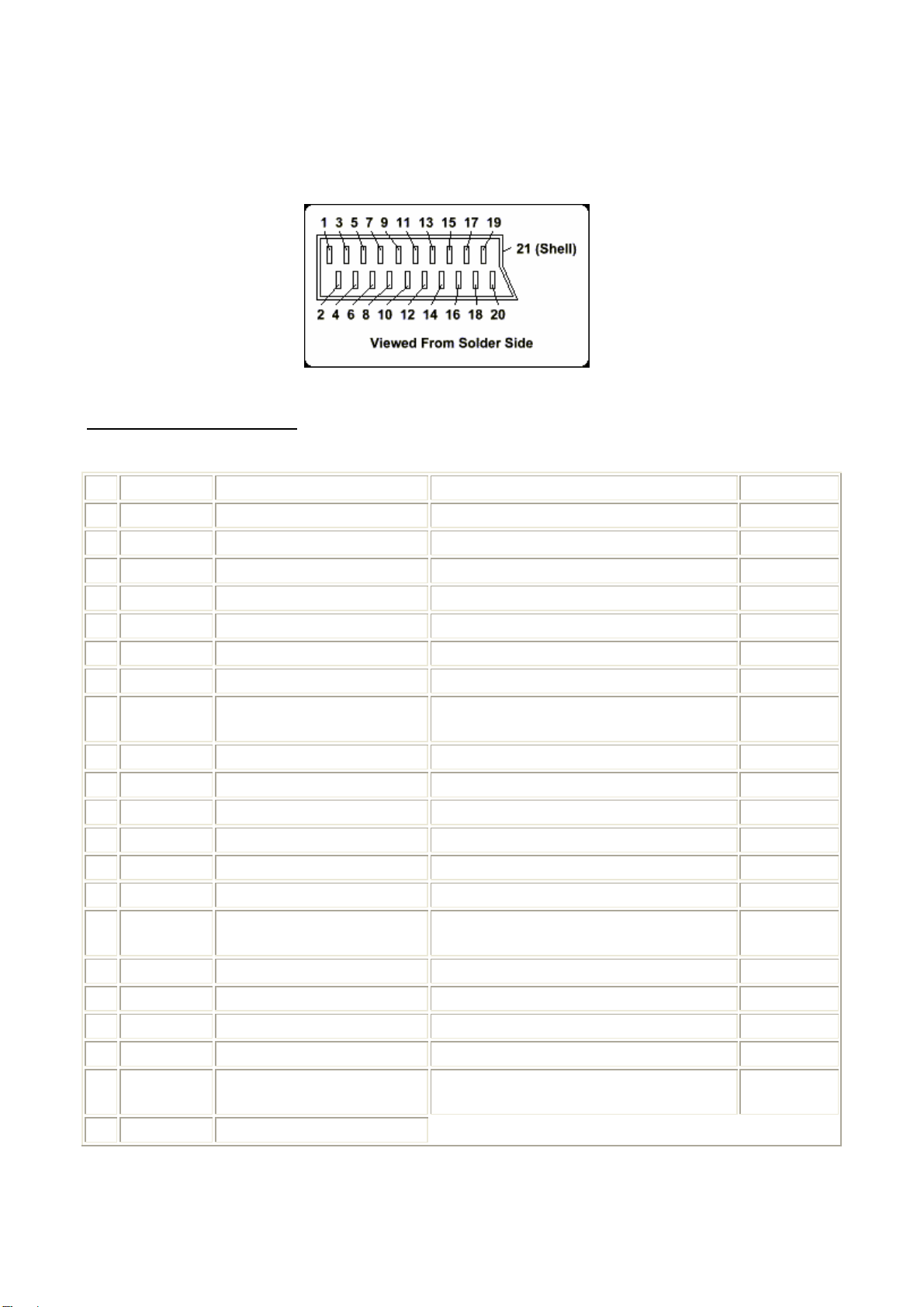
1. PERI- TV SOCKET (SCART)
PIN DETAILS OF SCART
Pin Name Description Signal Level Impedance
1 AOR Audio Out Right 0.5 V rms <1k ohm
2 AIR Audio In Right 0.5 V rms >10k ohm
3 AOL Audio Out Left + Mono 0.5 V rms <1k ohm
4 AGND Audio Ground
5 B GND RGB Blue Ground
6 AIL Audio In Left + Mono 0.5 V rms >10k ohm
7 B RGB Blue In 0.7 V 75 ohm
8 SWTCH Audio/RGB switch / 16:9
9 G GND RGB Green Ground
10 CLKOUT Data 2: Clockpulse Out Unavailable
11 G RGB Green In 0.7 V 75 ohm
12 DATA Data 1: Data Out Unavailable
13 R GND RGB Red Ground
0-2 V=TV, 5-8 V=WideScreen, 9.5-12
V=AV Mode
>10 kohm
14 DATAGND Data Ground
15 R
16 BLNK Blanking Signal 1-3 V=RGB, 0-0.4 V=Composite 75 ohm
17 VGND Composite Video Ground
18 BLNKGND Blanking Signal Ground
19 VOUT Composite Video Out 1 V 75 ohm
20 VIN
21 SHIELD Ground/Shield (Chassis)
RGB Red In /
Chrominance
Composite Video In /
Luminance
0.7 V (Chroma.: 0.3 V burst) 75 ohm
1 V 75 ohm
4

2. MICRO CONTROLLER AND SMALL SIGNAL FUNCTION WITH TDA 9351
combination of microcontroller and chroma (Small Signal function). This IC performs all important
functions in TV receiver. The details of IC are bifurcated in two parts. Small Signal function and
microcontroller
:- This IC is a
2A:- SMALL SIGNAL FUNCTION:
2A.1: VISION IF AMPLIFIER: The vision IF amplifier can demodulate signals with positive and
negative modulation. The PLL demodulator is completely alignment-free. The VCO of the PLL
circuit is internal, and the frequency is fixed to the required value by using the clock frequency
of the Controller/ Teletext decoder as a reference. The setting of the various frequencies (38,
38.9, 45.75 and 58.75 MHz) can be made via the control bits IFA-IFC in sub address 27H.
Because of the internal VCO, the IF circuit has a high immunity to EMC interferences.
2A.2: VIDEO SWITCHES:
The selected CVBS signal can be supplied to pin 38, the IF video output. The selection
The video switch has one input for an external CVBS or Y/C signal.
between both signals is realized by means of the SVO bit in sub address 22H. The video ident
circuit can be connected to the incoming ‘internal’ video signal or to the selected signal. This
ident circuit is independent of the synchronisation and can be used to switch the time-constant
of the horizontal PLL depending on the presence of a video signal (via the VID bit). Because of
the availability of the Y/C input and the subcarrier output an external comb-filter can be applied.
In that case an external video switch (or comb-filter with integrated switch) must be used. The
subcarrier output is combined with a 3-level output switch (0 V, 4 V and 8 V). The output level
and the availability of the subcarrier signal is controlled by the CMB1 and CMB0 bits. The
output can be used to switch sound traps etc.
2A.3: SOUND CIRCUIT (QSS VERSION)
The sound IF amplifier is similar to the vision IF amplifier and has an external AGC decoupling
capacitor. The single reference QSS mixer is realised by a multiplier. In this multiplier the SIF
signal is converted to the intercarrier frequency by mixing it with the regenerated picture carrier
from the VCO. The mixer output signal is supplied to the output via a high-pass filter for
5

attenuation of the residual video signals. With this system a high performance hi-fi stereo
sound processing can be achieved. The AM sound demodulator is realised by a multiplier. The
modulated sound IF signal is multiplied in phase with the limited SIF signal. The demodulator
output signal is supplied to the output via a low-pass filter for attenuation of the carrier
harmonics. The AM signal is supplied to the output (pin 44) via the volume control. It is possible
to get the AM output signal (not controlled on amplitude) on the QSS intercarrier output. The
selection is made by means of the AM bit in subaddress 29H. Another possibility is that pin 35
is transferred to external audio input pin and pin 32 to (non-controlled) AM output pin. This can
be realised by means of the setting the control bits CMB0 and CMB1 in subaddress 22H.
2A.4: FM DEMODULATOR AND AUDIO AMPLIFIER (MONO VERSIONS):-
demodulator is realised as narrow-band PLL with external loop filter, which provides the
necessary selectivity without using an external band-pass filter. To obtain a good selectivity a
linear phase detector and constant input signal amplitude are required. For this reason the
intercarrier signal is internally supplied to the demodulator via a gain controlled amplifier and
AGC circuit. The nominal frequency of the demodulator is tuned to the required frequency
(4.5/5.5/6.0/6.5 MHz) by means of a calibration circuit which uses the clock frequency of the
Controller/Teletext decoder as a reference. The setting to the wanted frequency is realised by
means of the control bits FMA and FMB in control byte 29H. When required an external sound
band-pass filter can be inserted in front of the narrow-band PLL. In that case pin 32 has to be
switched to sound IF input by means of the bits SIF (subaddress 21H) and CMB0/CMB1
(subaddress 22H). When the sound IF input is selected the subcarrier output or AVL function
are not available. From the output status bytes it can be read whether the PLL frequency is
inside or outside the window and whether the PLL is in lock or not. With this information it is
possible to make an automatic search system for the incoming sound frequency. This can be
The FM
realised by means of a software loop which switches the demodulator to the various
frequencies and then select the frequency on which a lock condition has been found. The
deemphasis output signal amplitude is independent of the TV standard and has the same value
for a frequency deviation of 25 kHz at the 4.5 MHz standard and for a deviation of 50 Khz for
the other standards. The audio control circuit contains an audio switch and volume control. In
the mono intercarrier sound versions, the Automatic Volume Levelling (AVL) function can be
activated. The pin to which the external capacitor has to be connected depends on the IC
version. For the 90 degree types the capacitor is connected to the EW output pin (pin 20). For
6

the 110 degree types a choice must be made between the AVL function and a sub-carrier
output for comb filter applications. This choice is made via the CBM0 and CMB1bits (in
subaddress 22H). When the AVL is active it automatically stabilises the audio output signal to a
certain level. The signal on the deemphasis pin (28) can be supplied to the SCART connector
via a buffer stage. It is also possible to use this pin as additional audio input. In that case the
internal signal must, of course, be switched off. This can be realised by means of the sound
mute bit (SM in subaddress 29H). When the IF circuit is switched to positive modulation the
internal signal on the deemphasis pin is automatically muted. The audio switch is controlled by
means of the INA/INB bits in subaddress 22H. It is, however, also possible to overrule the
audio switch position by means of the ADS and ADX bits (subaddresses 28H and 21H
respectively).
2A.5: SYNCHRONISATION CIRCUIT :-
and vertical sync pulses and a data-slicing circuit which extracts the digital teletext data from
the analog signal. The horizontal drive signal is obtained from an internal VCO which is running
at a frequency of 25 MHz. This oscillator is stabilised to this frequency by using a 12 MHz
signal coming from the reference oscillator of the micro controller/Teletext decoder. The
horizontal drive is switched on and off via the soft start/stop procedure. This function is realised
by means of variation of the T ON of the horizontal drive pulses. In addition the horizontal drive
circuit has a ‘low-power start-up’ function. The vertical synchronisation is realised by means of
a divider circuit. The vertical ramp generator needs an external resistor and capacitor. For the
vertical drive a differential output current is available. The outputs must be DC coupled to the
vertical output stage. In the types which are intended for 90 degree picture tubes the following
geometry parameters can be adjusted:
• Horizontal shift
• Vertical amplitude
• Vertical slope
The IC contains separator circuits for the horizontal
• S-correction
• Vertical shift
The types which are intended to be used in combination with 110 degree picture tubes have an
East-West control circuit in stead of the AVL function.
7

The additional controls for these types are:
• EW width
• EW parabola width
• EW upper and lower corner parabola correction
• EW trapezium correction
• Vertical zoom
2A.6: CHROMA AND LUMINANCE PROCESSING: -
(including the SECAM cloche filter) are realised by means of gyrators and are tuned to the right
frequency by comparing the tuning frequency with the reference frequency of the colour
decoder. The luminance delay line and the delay cells for the peaking circuit are also realised
with gyrators. The circuit contains a black stretcher function which corrects the black level for
incoming signals which have a difference between the black level and the blanking level.
2A.7: COLOUR DECODER :-
PAL/NTSC decoder does not need external reference crystals but has an internal clock
generator which is stabilised to the required frequency by using the 12 MHz clock signal from
the reference oscillator of the micro controller/Teletext decoder. Under bad-signal conditions
(e.g. VCR-playback in feature mode), it may occur that the colour killer is activated although
the colour PLL is still in lock. When this killing action is not wanted it is possible to overrule the
colour killer by forcing the colour decoder to the required standard and to activate the FCO-bit
(Forced Colour On) in subaddress 21H. The Automatic Colour Limiting (ACL) circuit
The IC can decode PAL, NTSC and SECAM signals. The
The chroma band-pass and trap circuits
(switchable via the ACL bit in subaddress 20H) prevents that over saturation occurs when
signals with a high chroma-to-burst ratio are received. The ACL circuit is designed such that it
only reduces the chroma signal and not the burst signal. This has the advantage that the colour
sensitivity is not affected by this function. The SECAM decoder contains an auto-calibrating
PLL demodulator which has two references, viz: the divided 12 MHz reference frequency
(obtained from the microcontroller) which is used to tune the PLL to the desired free-running
frequency and the bandgap reference to obtain the correct absolute value of the output signal.
The VCO of the PLL is calibrated during each vertical blanking period, when the IC is in search
or SECAM mode. The base-band delay line (TDA 4665 function) is integrated. This delay line
8

is also active during NTSC to obtain a good suppression of cross colour effects. The
demodulated colour difference signals are internally supplied to the delay line.
RGB OUTPUT CIRCUIT AND BLACK-CURRENT STABILIZATION : In the RGB control
2A.8:
circuit the signal is controlled on contrast, brightness and saturation. The ICs have a linear
input for external RGB signals. It is possible to use this input for the insertion of YUV signals.
Switching between RGB and YUV can be realised via the YUV-bit in subaddress 2BH. The
signals for OSD and text are internally supplied to the control circuit. The output signal has an
amplitude of about 2 Volts black-to-white at nominal input signals and nominal settings of the
various controls. To obtain an accurate biasing of the picture tube the ‘Continuous Cathode
Calibration’ system has been included in these ICs. A black level offset can be made with
respect to the level which is generated by the black current stabilization system. In this way
different colour temperatures can be obtained for the bright and the dark part of the picture.
The black current stabilization system checks the output level of the 3 channels and indicates
whether the black level of the highest output is in a certain window (WBC-bit) or below or
above this window (HBC-bit). This indication can be read from the status byte 01 and can be
used for automatic adjustment of the Vg2 voltage during the production of the TV receiver.
During switch-off of the TV receiver a fixed beam current is generated by the black current
control circuit. This current ensures that the picture tube capacitance is discharged. During the
switch-off period the vertical deflection is placed in an overscan position so that the discharge
is not visible on the screen.
2B. - MICROCONTROLLER WITH TELETEX DECODER: -
with embedded microcontroller is a control system designed for TV sets with analogue picture
and sound control. The system also offers an on screen display (OSD) and IR remote control of
all functions.
3. TUNER: tuning is based on frequency synthesis tunning.
GDC Tuner EWT 5F3T1 is controlled by I2C bus through IC TDA 9361.The
The integrated teletex decoder
9

CHANNEL COVERAGE :
BAND
CHANEL RANGE
LOW BAND E2- S9 48.25 – 161.25
MID BAND S10 – S41 168.25 – 463.25
HIGH BAND E21 – E69 471.25 – 855.25
4. VIDEO SWITCH BU 4052
main function of this device is to accept an AV input from SCART, external AV and switch the
required output at pin no Z which is applied to small signal processing IC.
5. SOUND PROCESSOR
The TDA 9859 selects signal from Three Stereo Sources or Six Mono Sources and out put
can be given to scart. The sound processor is I2C bus controlled and all settings of bus are
: TDA 9859 is designed to perform demodulation of FM TV sound.
OFF AIR CHANELS
FREQUENCY
: The HEF4052 is a dual four channel analog multiplexer. The
( IN MHZ)
stored in sub address register.
6. SOUND OUTPUT
It is supplied by 13 volts from the 13 volt DC coming from a separate winding in the SMPS
transformer. An out power of 1.5 Watt can be delivered into an 8 Ohm Load. This IC is also
having a feature of auto volume controller. Similarly stand by signal coming from
microcontroller is used to disable the sound out put from speaker.
7. VERTICLE OUTPUT STAGE
for 90 degree and 110 degree deflection systems . One supply voltage for the scan is
required. The drive voltage is amplified by an amplifier. The supply voltage of this IC is 15
Volts.
8. VIDEO OUTPUT AMPLIFIER
output amplifier section. IC TDA6107 or transistorized circuit can be used for video signal
: - IC AN17821 is used as the AF out amplifier for the Stereo application.
:- The STV 9302 is a vertical deflection circuit can be used
: The RBG output signal from TDA 9351 is applied to video
amplification and to be applied to cathodes of CRT for generation of R, G, and B colors. If IC
10

is used, then internal amplifiers are used to amplify the video signal. The transistorized
amplifier can be designed by using transistor circuit in which 9 transistors are used. Chassis
VE01 consist of transistorized video amplifier circuit.
9. POWER SUPPLY
SMPS transformer controlled by STR 0765, which is designed for deriving, controlling and
protecting switiching transistor of SMPS. The transformer produces 110 volts for FBT, 13 Volt
for audio O/p IC, 33 Volts for tuner and 5 and 8 Volts regulated voltages through IC TA7805
and TA7808.
10. MEMORY IC
EEPROM organized as 128 pages X 16 bytes. This is compatible with I2C standards, two
wire serial interface which uses a bi directional data bus and serial clock.
: The DC Voltages required at various part of the chassis are applied by
: The 24C16 is a 16 Kilo Bit electrically erasable programmable memory.
11
 Loading...