

Roadstar CLT-700 Service Manual
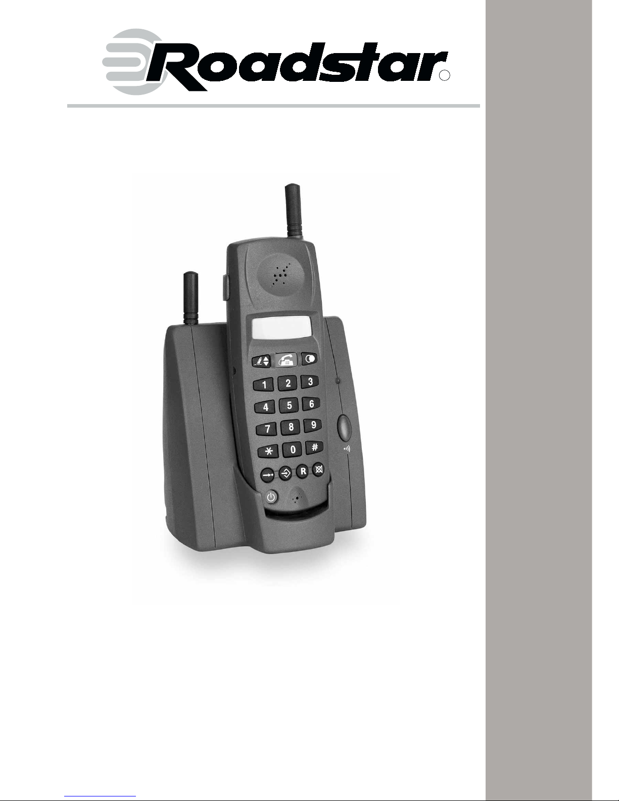
Service Manual - CLT-700
Service Manual - CLT-700
CLT-700
R

1. DESCRIPTION OF EQUIPMENT
1. TYPE OF THE CIRCUIT
A. BASE UNIT RECEIVER ; Double conversion superheterodyne receiver
B. HANDSET RECEIVER ; Double conversion superheterodyne receiver
2.
FREQUENCY AND CHANNELS
A. BASE UNIT CT1 CT1+
TX 959.0125 – 959.9875MHz 930.0125MHz – 931.9875MHz
RX 914.0125 – 914.9875MHz 885.0125MHz – 886.9875MHz
B.HANDSET
TX 914.0125 – 914.9875MHz 885.0125MHz – 886.9875MHz
RX 959.0125 – 959.9875MHz
930.0125MHz – 931.9875MHz
C. CHANNELS 40 80
D. CH SPACING 25KHz 25KHz
3. TRANSMIT POWER : 10mW
4. OPERATING VOLTAGE
A. BASE UNIT ; AC 230V / 50Hz
B. HANDSET ; DC 3.6V
5.
OPERATING TEMPERATURE
: 0 ~ 55 C

2. CIRCUIT DESCRIPTION
A. BASE UNIT
1. Power supply circuit
The DC 9V from the AC adaptor is supplied to JP3 (DC modular jack).
This input voltage is supplied to the main circuit through D8 (diode) and supplied to the
charge circuit.
The voltage from D8 is regulated to 5V by regulator U9. This regulated 5V is supplied
to main circuit and RF circuit.
2. Charging circuit
Charging circuit is composed of U11, Q11, Q12, R99, R100, R102, R103 and R104.
This charging circuit supplies constant current to the handset batteries through CHG+1
and CHG-1.
When the charge current flows through R100, U11 (photo-coupler) detects the current
and send a CHARGE signal to pin 23 of U4 (CPU).
Then LD4 (VISION) or LD6 (INNO)1 is lighted by the command from CPU (pin 28)
LED_CHG.
3. Receiving audio signal from telephone line
The audio signal from JP1 (telephone line modular jack) goes pin 1 of U1 (speech
network) through bridge diode composed of D1, D2, D3 and D4, C814 and switching
transistor Q3.
After being amplified in speech network, it comes out from pin 4 and goes to the pin8 of
U10 (compander) through R81 and C62.
This signal is amplified and compressed for noise reduction then goes through 3rd
order low pass filter composed of op amp in U10, C52, C53, C54 R72, R73 and R74.
This signal is sent to the modulation input (MOD_AUDIO) of the RF block through C51,
R70 and RV3 and transmitted to the handset.
4. Sending audio signal to telephone line
Received RF signal from handset is detected in the RF block and the demodulated
audio signal (DEMOD_AUDIO) is filtered by low pass filter composed of U8A, C41,
C42, C43, R57, R58 and R59 through C44. This audio signal is filtered again by
high pass filter composed of op amp in U10, C37, C38, C39, R53, R54 and R55 then
expanded in U10.
The expanded signal coming from pin 19 of U10 goes to the pin 6 and 7 of U1 (speech
network) through C34 and R52.

Speech network adjusts a transmit signal gain and sends it to the telephone line
through switching transistor Q3, bridge diode (D1, D2, D3 and D4) and modular jack
JP1.
5. Sending and Receiving of data signal
The sending MSK data comes out from TX_DATA of CPU (pin 43), and enters into pin
4 of U10 (compander).
It is modulated at RF block through the same path as audio signal.
The received MSK data which demodulated at RF block with the same manner as
audio signal is going to the low path filter composed of U8C, C47, C48, C49, R64, R65
and R67. Filtered signal is comparated at U8D. The square wave from U8D(RX_DATA)
is fed to pin 44 of CPU.
6. Ring detector circuit
When the ring signal is supplied to U2(photo coupler) through C1, R1, DZ1, DZ2 and
R3, U2 detects it and send a RING_SIGNAL signal to pin 31 of U4 (CPU).
Then the base unit sends a ringing data through the "sending data path" to the
handset.
7. Line detect circuit
If the telephone line is connected, the Q2 will be on, LINE_DETECT signal become low
level. Then CPU knows that tel-line is connected.
If the telephone line is not connected or higher priority telephone is operated, the Q2
will be off and CPU knows that tel-line is not connected or higher priority telephone is
operating.
This function is factory settable option.
8. DTMF signal
In case that the phone is in tone dialing mode, it is possible to use DTMF dial.
DTMF signal is generated by U3 by the command of D0, D1, D2 and D3 from CPU
(pin 11, 12, 13, and 14).
DTMF signal from U3 (pin 14) is supplied to the pin 11 of U1 and sent to the telephone
line.
9. Pulse dialing
In case that the phone is in pulse dialing mode, it is possible to use pulse dial.
The pulse signal is made by switching Q3 (switching TR) on and off by
PULSE_CON(CPU pin 30).

During the pulse comes out, the CPU makes the Q5 on by maintaining PPD_CON (pin
25 of CPU) high, in this time the switching board will acknowledge the dial clearly by
the occurance of the low impedance.
10. EEPROM
U6 is the EEPROM.
This stores the identification code which are inherent to pair of base unit and handset
to safe guard against interference. It also stores telephone numbers for memory dial.
11. Reset circuit
Reset is applied by connecting an external capacitor C70 and a diode D7.
12. Speech network
R20, R21,C16, C17, and C18 are used for impedance matching between telephone
line and phone.
The resistors and capacitors connectors connected pin10, 16 of U1 are for side tone
balance.

B. Base RF Section
Frequencies
[ CT1 ]
RX VCO
Base unit : f
VCO
= (fRX - 21.7MHz) / 2 = 446.39375MHz (20CH)
Handset : f
VCO
= (fRX + 21.7MHz) / 2 = 490.59375MHz (20CH)
LOCA
L
Base unit : f
LOCAL
= fRX - 21.7MHz = 892.7875MHz (20CH)
Handset : f
LOCAL
= fRX + 21.7MHz = 981.1875MHz (20CH)
TX VCO
Base unit : f
TX
2 = 479.74375MHz (20CH)
Handset : f
TX
2 = 457.24375MHz (20CH)
cf. Base unit : f
RX
= 914.4875MHz / fTX = 959.4875MHz (20CH)
Handset : fRX = 959.4875MHz / fTX = 914.4875MHz (20CH)
[ CT1+ ]
RX VCO
Base unit : f
VCO
= (fRX - 21.7MHz) / 2 = 432.14375MHz (40CH)
Handset : f
VCO
= (fRX + 21.7MHz) / 2 = 476.34375MHz (40CH)
LOCAL
Base unit : f
LOCAL
= fRX - 21.7MHz = 864.2875MHz (40CH)
Handset : f
LOCAL
= fRX + 21.7MHz = 952.6875MHz (40CH)
TX VCO
Base unit : f
TX
2 = 465.49375MHz (40CH)
Handset : f
TX
2 = 442.99375MHz (40CH)
cf. Base unit : f
RX
= 885.9875MHz / fTX = 930.9875MHz (40CH)
Handset : fRX = 930.9875MHz / fTX = 885.9875MHz (40CH)

1. RX VCO circuit
RX VCO circuit is configured by Q305, Q306, D302 (varicap diode), L301 (air coil), and
some additional passive parts.
The control voltage from pin 14 (charge pump out) of the U302 (PLL IC) is supplied to
the D302 cathode through passive loop filter (C336, C337, C338, R329, R330, R331)
to control the oscillation frequency.
L301 is used to adjust the oscillation frequency band.
The oscillation frequency of 450MHz band signal goes to pin 16 of U302 via C345.
The oscillator output is doubled by Q305 (doubler) and fed into Q303 (RX mixer).
2. TX VCO circuit
TX VCO circuit is configured by Q307, D303, L302 and some additional passive parts.
The control voltage from pin 3 (charge pump out) of the U302 is supplied to the D303
cathode through passive loop filter (C353, C354, C355, R338, R339, R340) to control
the oscillation frequency.
The modulating signal (MOD_AUDIO) is supplied to D303 anode.
L302 is used to adjust the oscillation frequency band.
The oscillation frequency of 450MHz band signal goes to pin 1 of U302 via C363.
The doubled frequency of the 450MHz is taken out from the Q308 (doubler) collector
side and fed to the transmission section of the next stage composed of Q309 (driver
amp) and Q310 (power amp).
The Q307 of VCO and Q308, Q309 is powered through the Q9 by the command of
VCO_CON of the CPU (pin 34).
Q310 is powered through the Q8 by the command of AMP_CON of CPU (pin 35).
3. PLL (phase locked loop) Section
U302 is a dual PLL IC which has two PLL circuits each one for the transmitter and
receiver sections.
Frequency signal of 450MHz band from the VCO is supplied to pins 1 (TX) and pin 16
(RX), and it is divided down to 6.25KHz in accordance with the frequency division ratio
assigned by CPU .
Reference frequency 6.25KHz is made by dividing X301 (21.2503MHz) in accordance
with reference frequency division ratio assigned by CPU.
Voltage of the frequency error comes from pin 3(TX), 14(RX) of U302 as a DC signal.
These voltage are supplied to D303 of the transmitter VCO and D302 of the receiver
VCO and the VCO frequencies are locked to 6,25KHz reference frequency.
The pin 6,7 and 8 of U302 are the serial data inputs for the frequency divider deciding
the division ratio.

Carrier frequency is adjusted correctly by CV301.
4. Receiver RF section
Modulated RF carrier from the antenna is filtered by F306 and amplified by Q304.
Amplified signal is filtered again by F307.
RF carrier and RX local oscillator output from Q305 are mixed at Q303 (1st mixer),
then the signal is converted into the 21.7MHz (1st IF frequency).
After having been restricted to ±7.5KHz bandwidth by F302 (x-tal filter) and amplified
by Q302 (IF amplifier), the signal is fed to pin 16 of U301 (IF IC).
The second local oscillator signal is supplied to pin 1 of U301 from pin 9 of U302.
Here, received signal is converted into the 450KHz (2nd IF frequency) after passed
through 2nd mixer in U301.
It is detected and appears at pin 9 of U301 as a demodulated audio signal.
And this demodulated signal is adjusted to maximum output level and minimum
distortion by T301 (quardrature coil).
Demodulated audio signal is filtered by low pass filter composed of R301 and C301.
5. Transmitter RF section
The modulated output carrier from TX VCO is frequency doubled to TX frequency by
Q308, and amplified by Q309 and Q310, and transmitted to the antenna. The power is
10mw max. at the antenna terminal. The F305 provides filtering so that spurious
signal from the transmission side cannot be radiated to the antenna.
6. Squelch circuit
When the RF signal doesn't exist, the noise of pin 9 on the U301 increases then 6KHz
band pass filter composed of op amp in U101 ( pin10, pin11 ) and some passive parts
picks up the noise and the Q312 amplifies it . The rectifier circuit composed of D301,
R308 and C313 rectifies the noise to DC voltage. When the rectified output voltage is
over 0.7V, pin 13 of U301 becomes low then CPU (pin32) knows that received RF
signal is very weak or there is no RF signal.
When the RF signal exists, the noise of pin 9 on the U301 reduces. So the rectified
output voltage goes below 0.7V, then pin 13 of U301 becomes high. CPU knows that
RF signal exist.

C. Handset
1. Power control circuit
3.6V DC power is supplied from the battery through JP2.
U4 has 3 regulated outputs (VREG0, 1, 2) controlled by BS0, BS1 and BS2
respectively.
In receiving mode, the BS0 (pin 23 of U5) becomes low, then the receiver part of RF
block is supplied with the power of 3.2V from VREG0 (pin 15 of U4).
In transmitting mode, the BS1 (pin 24 of U5) becomes low, then the transmitter part of
RF block is supplied with the power of the 3.2V from VREG1 (pin 1 of U4).
On the other hand PLL, MSK data filter(U3A, U3B), EEPROM, key pad, charge
detector, CPU reset circuit, low battery detector circuit and CPU are supplied with the
power of the 3.2V from VREG2 (pin 5 of U4).
VREG2 always comes out 3.2V output on power ON mode.
U1 (speak amplifier) and Q310 (final amplifier TR of transmitter RF block) are supplied
from battery directly for good efficiency. (V_BATT)
2. Low battery detector circuit
When the battery voltage drops below 3.2V, pin 10 of U4 (BATT_LOW) is driven to
high, so pin 57 of CPU is set to high, and then CPU (pin 17, 25) send warning tone
command to BZ1 (buzzer).
3. Receiving audio signal from base unit
Received RF signal from base unit is detected in the RF block and the demodulated
audio signal (DEMOD_AUDIO) is filtered by low pass filter composed of U3C, C13,
C14, C15, R7, R8 and R9 through C16. This audio signal is filtered again by high pass
filter composed of op amp in U2, C9, C10, C11, R3, R4 and R5 then expanded in U2.
The expanded signal coming from pin 19 of U2 is fed into a speaker amplifier U1 via
C6 and R2. The fully amplified audio signal is sent to the loud speaker (SP1).
When the user set the handset volume LOW, VOL_CONT from pin27 of CPU (U5) is
high level then Q2 is switched on. So C5 is connected to GND and the audio signal
from U2 is attenuated about 6dB
4. Sending audio signal to base unit
The audio signal picked up by the microphone (MI1) is fed into pin8 of U2 (compandor).
This signal is amplified and compressed for noise reduction then goes through 3rd
order low pass filter composed of op amp in U2, C18, C19, C20, R12, R13 and R14.
This signal is sent to the modulation input (MOD_AUDIO) of the RF block through C17,
R11 and RV2, and transmitted to the base unit.

5. Sending and Receiving of data signal
The sending MSK data comes out from TX_DATA of CPU (pin 49), and enters into pin
4 of U2(compandor).
It is modulated at RF block through the same path as audio signal.
The received MSK data which is demodulated at RF block with the same manner as
audio signal is going to the low path filter composed of U3B, C32, C33, C34, R30, R31
and R32. Filtered signal is comparated at U3A. The square wave (RX_DATA) from Q3
is fed to pin 48 of CPU.
6. Reset
When power switch (SW1) is pushed, pin 9 of U4 (RESET) is set from high to low.
This signal is used for CPU reset.
7. Power ON/OFF circuit
In case of setting power ON, if SW1 (power switch) is pushed, Q6 is ON then BS2
(pin12 of U4) becomes low level and VREG2 gives 3.2V power. The CPU is supplied
with this power of 3.2V(VREG2) and set BS2_CONT (pin 37 of CPU) to high level.
Then Q7 is switched ON, so BS2 remains low level even after SW1 is released.
In case of setting power OFF, if SW1 is pushed, pin 10 of CPU (PWR_OFF) becomes
high level and CPU makes BS0, BS1 and BS2_CON open state then all power is off.
In case that handset is put on charger cradle of base unit, automatically power
becomes ON because Q5 is ON.
8. Buzzer circuit
When the ring signal command comes from the base unit or the key pad is pushed, the
buzzer control signal comes from RING_ON of CPU (pin 17) and it makes Q12 ON and
OFF, then the buzzer (BZ1) makes ring or beep sound.
If the RING_LEVEL (pin 25 of U5) is set on high, then R42 is connected to R41 in
parallel and the sound will be loud.
And if the buzzer H/L is set on low, then the sound will be low.
9. Charge and detect circuit
If handset is cradled at base unit, the charge current is supplied from base unit through
the JP2 (charge contact). Charging current flows to the battery through D1.
At that time the Q4 will be on and the CHARGE of CPU (pin 22) become low, then the
CPU acknowledges the condition of charging.
 Loading...