

Page 1

RIGOL
User’s Guide
DS6000 Digital Oscilloscope Demo Board
July 2011
RIGOL Technologies, Inc.
Find Quality Products Online at: [email protected]
www.GlobalTestSupply.com
Page 2

RIGOL
II
Contents
Guaranty and Declaration ..................................................................................................... I
Chapter 1 Overview ....................................................................................................... 1-1
Chapter 2 Quick Start .................................................................................................... 2-1
2.1 Demo Board Layout .......................................................................................................2-1
2.2 Measurement Connection ...............................................................................................2-7
2.3 Demo Board Power-on ...................................................................................................2-7
Chapter 3 Demo Board Applications ............................................................................... 3-1
3.1 Common Signal Applications ...........................................................................................3-1
3.1.1 Square Signal .......................................................................................................3-1
3.1.2 Sine Signal ..........................................................................................................3-2
3.1.3 DA Output Signal..................................................................................................3-4
3.1.4 Differential Signal .................................................................................................3-6
3.1.5 PAL Video Signal ..................................................................................................3-8
3.1.6 NTSC Video Signal ................................................................................................3-9
3.1.7 Amplitude Modulation Signal ................................................................................ 3-10
3.2 Special Signal Applications ............................................................................................ 3-12
3.2.1 Noisy Sine Signal ................................................................................................ 3-12
3.2.2 Slow Sweep Signal ............................................................................................. 3-15
3.2.3 Fast Sweep Signal .............................................................................................. 3-17
3.2.4 Phase Deviation Signal ........................................................................................ 3-19
3.2.5 Rare Abnormal Signal ......................................................................................... 3-20
3.2.6 Frequent Abnormal Signal ................................................................................... 3-22
3.2.7 Manual Abnormal Signal ...................................................................................... 3-24
3.2.8 Manual Burst Signal ............................................................................................ 3-25
3.2.9 Narrow Burst Signal ............................................................................................ 3-27
3.2.10 Glitch Signal of Sine .......................................................................................... 3-28
3.2.11 Glitch Signal of Square Waveform ...................................................................... 3-30
3.2.12 Crosstalk Signal ................................................................................................ 3-32
3.3 Digital Signal Applications ............................................................................................. 3-35
3.3.1 RS232/UART Signal ............................................................................................ 3-35
3.3.2 SPI Signal .......................................................................................................... 3-38
3.3.3 I2C Signal .......................................................................................................... 3-40
3.3.4 CAN Signal ........................................................................................................ 3-42
3.3.5 Signals for Testing Logic Analyzer ........................................................................ 3-43
Find Quality Products Online at: [email protected]
www.GlobalTestSupply.com
User’s Guide for DS6000 Demo Board
Page 3

Chapter 1 Overview RIGOL
Chapter 1 Overview
This manual introduces the functions and using methods of DS6000 Demo board. This Demo board is
used to illustrate the basic functions of the oscilloscope. It is powered through USB port and can output
25 kinds of signals for the illustration of oscilloscope functions.
25 kinds of signals:
Common Signals
Square waveform
Sine waveform
Digital-to-analog (DA) signal
Unfiltered digital-to-analog (DA) signal
Differential Signal
PAL video signal
NTSC video signal
Amplitude modulation (AM) signal
Special Signals
Sine signal superimposed with noise
Slow sweep signal
Fast sweep signal
Phase deviation signal
Rare abnormal signal
Frequent abnormal signal
Manual abnormal signal
Manual burst
Narrow pulse
Sine signal superimposed with glitch
Square signal superimposed with glitch
Crosstalk signal
Digital signal
RS232/UART signal
I2C signal
SPI signal
CAN signal
Signals for testing logic analyzer
Note: introductions in this edition are based on the V2.1 version demo board.
Find Quality Products Online at: [email protected]
User’s Guide for DS6000 Demo Board 1-1
www.GlobalTestSupply.com
Page 4
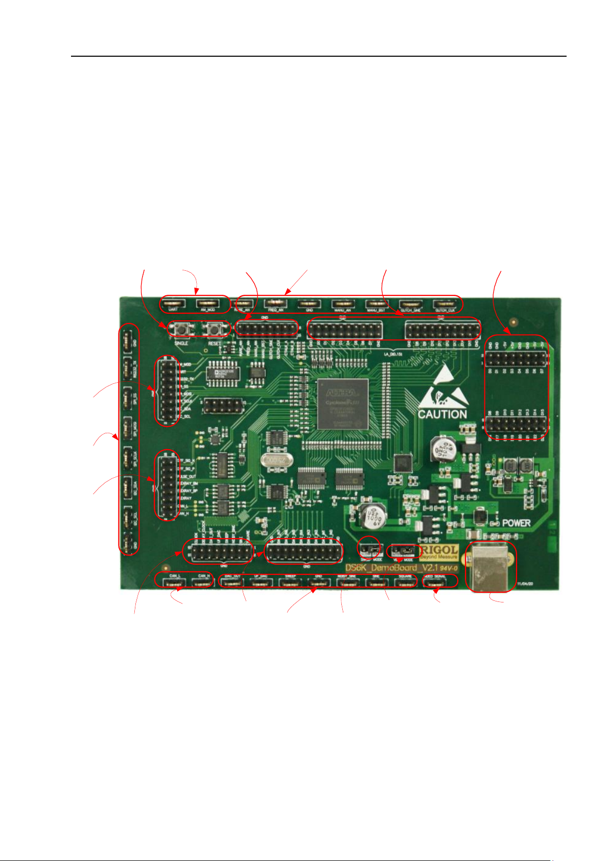
Chapter 2 Quick Start RIGOL
Part1 Part2_EPart2
Part3
Part3_E
Part3_E
Part4
Part4_E
Part5
Part5_E
Part6
Part5_S
Part7_S Part7_E
Part8
Part9
Part10
Chapter 2 Quick Start
This chapter briefly introduces the layout, the connection and the power-on of the Demo board.
2.1 Demo Board Layout
Figure 2-1 Board Layout
Find Quality Products Online at: [email protected]
User’s Guide for DS6000 Demo Board 2-1
www.GlobalTestSupply.com
Page 5
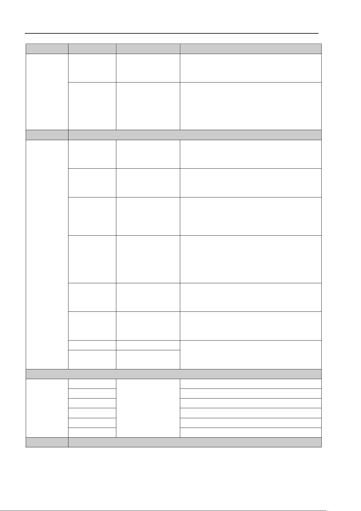
RIGOL Chapter 2 Quick Start
2-2
Diagrams
Pins
Definitions
Detailed Explanations
Part1
SINGLE
Manual trigger key
Used to trigger manual abnormal signal
(MANU_AN), manual Burst signal (MANU_BST)
and crosstalk signal.
RESET
Manual reset key
Press this key to reset the MCU on the Demo
board. When protocol (such as CAN) signal error
occurs due to MCU program runaway, press this
key to bring the MCU system back to normal
working state.
Part2
RARE_AN
Rare abnormal
signal
Output a 1MHz square waveform. Narrow pulse
occurs every 100ms and the pulse width is not
greater than 5 ns.
FREQ_AN
Frequent abnormal
signal
Output a 1MHz square waveform. Narrow pulse
occurs every 1ms and the pulse width is not
greater than 5 ns.
MANU_AN
Manual abnormal
signal
Controlled by the manual trigger key SINGLE.
Apart from the 1.25MHz square waveform, a
narrow pulse with 40ns pulse width is also
output each time the SINGLE key is pressed.
MANU_BST
Manual Burst
signal
Output 25 bursts each time the SINGLE key is
pressed. Each burst contains 100cyc high level,
3cyc low level, 1cyc high level, 3cyc low level
and 100cyc high level. The time of each cyc is
8ns.
GLITCH_SINE
Sine glitch signal
Output 500kHz sine signal on which glitches with
2ns width are superimposed. The glitch occurs
about every 90 us and its position is not fixed.
GLITCH_CLK
Square glitch signal
Output 1MHz square signal on which glitches
with 2ns width are superimposed. The glitch
position is not fixed.
CTALK_A
Crosstalk signal 1
Output 1MHz low-frequency square waveform.
A 125MHz high-frequency crosstalk signal is also
output each time the SINGLE key is pressed.
CTALK_B
Crosstalk signal 2
Part2_E
RARE_AN
Part2 pins extension
——
FREQ_AN
——
MANU_AN
——
MANU_BST
——
GLITCH_SINE
——
GLITCH_CLK
——
Table 2-1 Board Layout Explanation
Find Quality Products Online at: [email protected]
www.GlobalTestSupply.com
User’s Guide for DS6000 Demo Board
Page 6
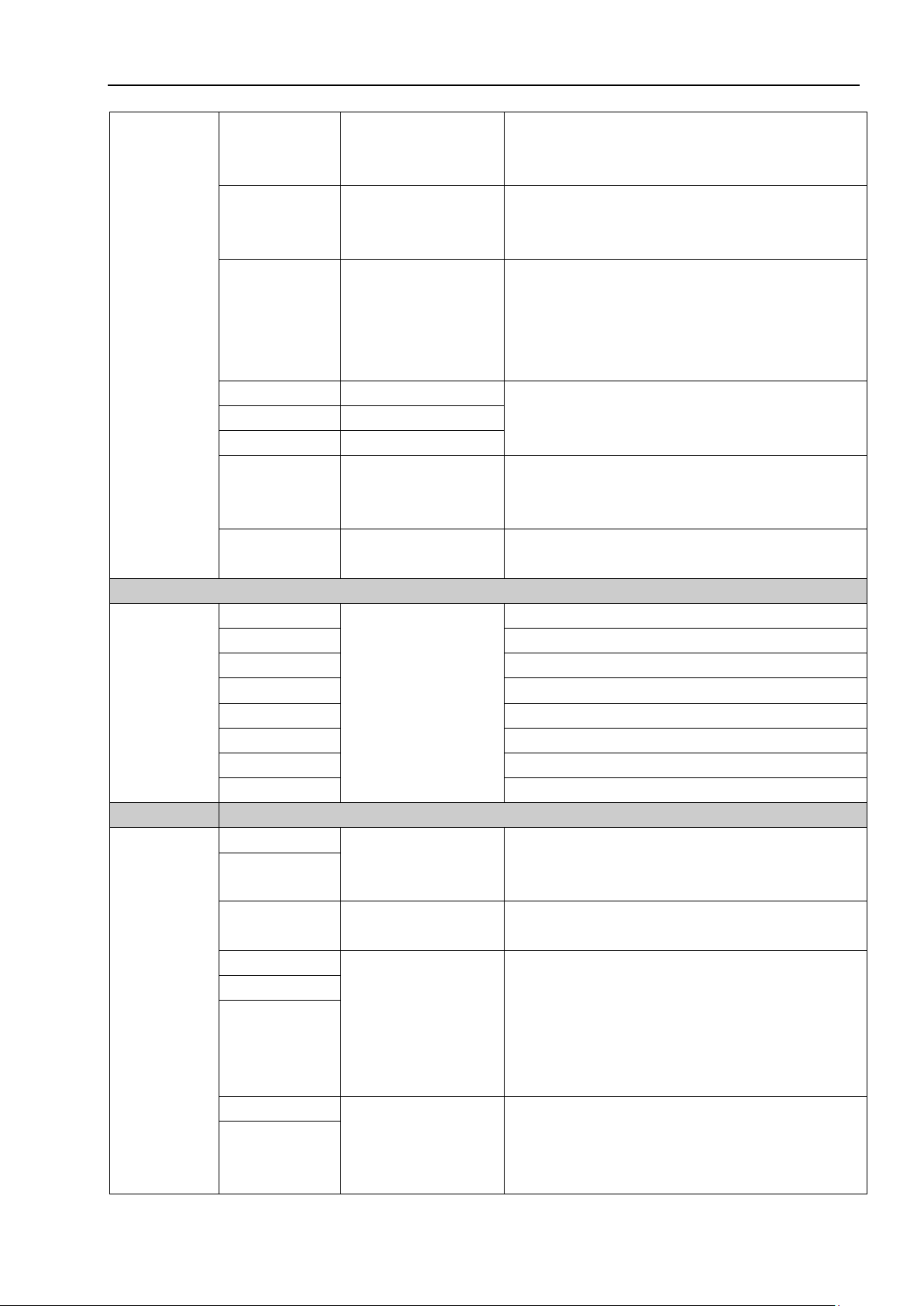
Chapter 2 Quick Start RIGOL
Part3
AM_MOD
Amplitude
modulation signal
Output amplitude modulation signal with 500kHz
carrier frequency and 10kHz modulating
frequency.
UART
Asynchronous serial
transmission signal
The output signal shares the same
characteristics (except polarity (positive
polarity)) with the signal output from RS232_TX.
RS232_TX
RS232 signal
Output a RS232 signal with 9600Bps baud rate,
1 start bit, 8 data bits, 1 stop bit, LSB output,
negative polarity and none check bit. The
content of the output data is the character string
“RIGOL DS6000”.
SPI_SS
SPI SS signal
The signal rate is 1.25MHz and the output data
steadily increases from 0 to 255.
SPI_MOSI
SPI MISO signal
SPI_SCLK
SPI MOSI signal
I2C_SDA
I2C data signal
Output signal of I2C data bus. The content of
the data is the character string “RIGOL” but the
data frame head and read/write bits will change.
I2C_SCL
I2C clock signal
Clock signal of I2C protocol. The clock frequency
is 125kHz.
Part3_E
AM_MOD
Part3 pins extension
——
UART
——
RS232_TX
——
SPI_SS
——
SPI_MOSI
——
SPI_SCLK
——
I2C_SDA
——
I2C_SCL
——
Part4
DIFF_SIG_N
Differential signal
Output random sequence. The frequency is
25MHz and the level logic is low-voltage
differential signal (LVDS).
DIFF_SIG_P
PULSE_OUT
Narrow pulse output
Output pulse signal with 100us period and 2ns
pulse width.
FLEXRAY_BM
Test signal of
FlexRay
vehicle-carried
network
communication
protocol
Not supported.
FLEXRAY_BP
FLEXRAY
CAN_L
Differential data bus
of CAN protocol
Output CAN signal with 1MHz signal rate. Its
data frame ID is 0x6C7, the data frame length is
5 Bytes and the data is the character string
“RIGOL”.
CAN_H
(Continued) Table 2-1 Board Layout Explanation
Find Quality Products Online at: [email protected]
User’s Guide for DS6000 Demo Board 2-3
www.GlobalTestSupply.com
Page 7
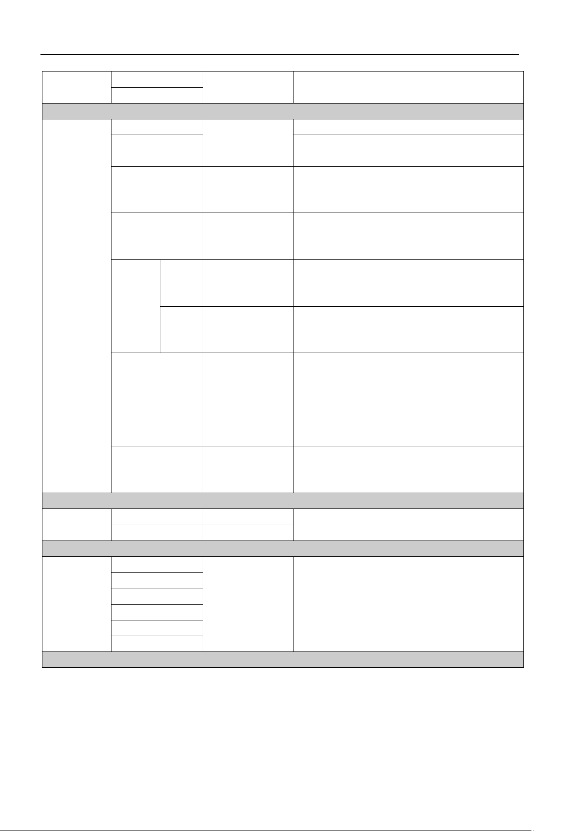
RIGOL Chapter 2 Quick Start
2-4
Part4_E
CANL
Part4
pins extension
——
CANH
Part5
CLOCK
Phase deviation
signal
50mV, 1MHz clock signal.
DELAY_CLOCK
660mV, 1MHz clock signal. The delay time
cannot exceed 4ns.
DAC_OUT
Digital-to-analog
output
8 bits digital signal with 10kHz signal frequency
and 25MHz sample frequency. Output the
converted and filtered sine waveform.
UF_DAC
Unfiltered
digital-to-analog
output
8 bits digital signal with 10kHz signal frequency
and 25MHz sample frequency. Output the
converted and unfiltered sine waveform.
SWEEP
SLOW
Slow sweep
Output a sweep signal of which the frequency is
from 1kHz to 100kHz. The sweep period is 40s
and the sweep mode is log.
FAST
Fast sweep
Output a sweep signal of which the frequency is
from10kHz to 1MHz. The sweep period is 8s and
the sweep mode is log.
NOISY_SINE
Noisy sine signal
Output sine signal with 500kHz frequency and
1Vpp amplitude. A sine waveform with 125MHz
frequency and 300mVpp amplitude is
superimposed on this sine signal.
SINE
Sine
Output sine signal with 500kHz frequency and
1Vpp amplitude.
SQUARE
Square
Output square waveform signal with 1MHz
frequency, 3.3Vpp amplitude, 50% duty cycle
and 10% overshoot.
Part5_S
SLOW
Slow sweep
Select “Slow” or “Fast” sweep.
FAST
Fast sweep
Part5_E
DAC_OUT
Part5
pins extension
——
UF_DAC
SWEEP
NOISY_SINE
SINE
SQUARE
(Continued) Table 2-1 Board Layout Explanation
Find Quality Products Online at: [email protected]
www.GlobalTestSupply.com
User’s Guide for DS6000 Demo Board
Page 8
Chapter 2 Quick Start RIGOL
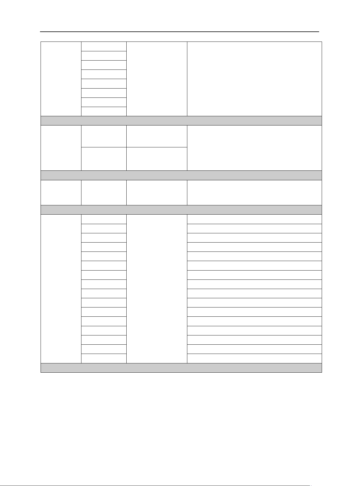
Part6
DAC_IN7
Digital-to-analog
input
Provide 8 bits digital signal as DAC input.
DAC_IN6
DAC_IN5
DAC_IN4
DAC_IN3
DAC_IN2
DAC_IN1
DAC_IN0
Part7_S
NTSC
NTSC video signal
Select the standard of the output signal of the
VIDEO_SIGNAL pin. Select NTSC to output a
NTSC video signal. Select PAL to output a
PAL/SECAM video signal. The signal amplitude is
1Vpp.
PAL
PAL video signal
Part7_E
VIDEO_SIGNA
L
Video signal output
——
Part8
LA_D0
Signals for testing
Logic analyzer,
16-channel parallel
data
Output 12.5MHz square waveform.
LA_D1
Output 6.25MHz square waveform.
LA_D2
Output 3.125MHz square waveform.
LA_D3
Output 1.562MHz square waveform.
LA_D4
Output 781.2kHz square waveform.
LA_D5
Output 390.6kHz square waveform.
LA_D6
Output 195.3kHz square waveform.
LA_D7
Output 97.66kHz square waveform.
LA_D8
Output 48.83kHz square waveform.
LA_D9
Output 24.4kHz square waveform.
LA_D10
Output 12.2kHz square waveform.
LA_D11
Output 6.1kHz square waveform.
LA_D12
Output 3.05kHz square waveform.
LA_D13
Output 1.525kHz square waveform.
LA_D14
Output 762.2Hz square waveform.
LA_D15
Output 381.1Hz square waveform.
(Continued) Table 2-1 Board Layout Explanation
Find Quality Products Online at: [email protected]
User’s Guide for DS6000 Demo Board 2-5
www.GlobalTestSupply.com
Page 9
RIGOL Chapter 2 Quick Start
2-6
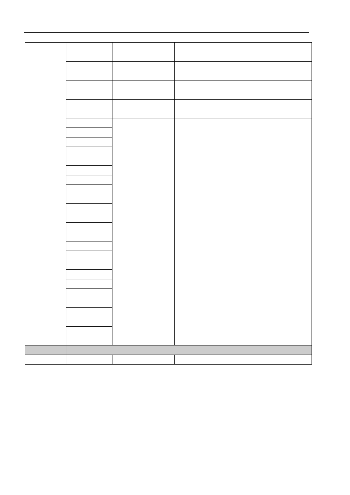
Part9
GND
Ground terminal
——
GND
Ground terminal
——
+5V
+5V DC voltage
——
+5V
+5V DC voltage
——
GND
Ground terminal
——
GND
Ground terminal
——
-5V
-5V DC voltage
——
-5V
-5V DC voltage
——
D0
24 bits digital input
terminal
24 bits digital input terminal. It can input digital
data stream and be used for function extension.
D1
D2
D3
D4
D5
D6
D7
D8
D9
D10
D11
D12
D13
D14
D15
D16
D17
D18
D19
D20
D21
D22
D23
Part10
——
USB Device
USB port, used for demo board power supply.
(Continued) Table 2-1 Board Layout Explanation
Find Quality Products Online at: [email protected]
www.GlobalTestSupply.com
User’s Guide for DS6000 Demo Board
Page 10
Chapter 2 Quick Start RIGOL
2.2 Measurement Connection
Connect the signal output terminals of the Demo board to the corresponding input terminals of the
oscilloscope before using the Demo board.
Connection Method:
1. Connect the BNC terminal of the probe to one of the BNC connectors of input channels (CH1-CH4) at
the front panel of the oscilloscope.
2. Connect the probe tip to the corresponding signal output pin on the Demo board and connect the
ground alligator clip of the probe to the ground terminal (GND) of the Demo board.
2.3 Demo Board Power-on
The Demo board can be powered through the USB port. Connect the USB DEVICE interface of the Demo
board with the USB HOST interface of the oscilloscope or PC using USB data cable.
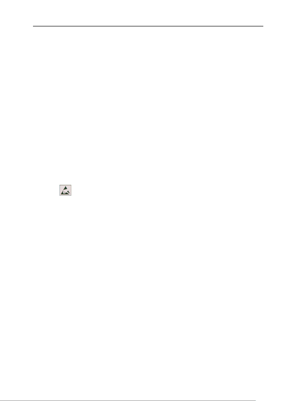
Note: The icon at the upper-right corner of the board indicates that static electricity would cause
Demo board damage and the board should be used in anti-static environment as far as possible.
Find Quality Products Online at: [email protected]
User’s Guide for DS6000 Demo Board 2-7
www.GlobalTestSupply.com
Page 11
Chapter 3 Demo Board Applications RIGOL
Duty Cycle Measurement
Chapter 3 Demo Board Applications
In this chapter, the Demo board is used to demonstrate the functions of the oscilloscope and the
demonstration results of 25 kinds of signals are presented.
3.1 Common Signal Applications
3.1.1 Square Signal
1. Signal Explanation
Signal Output Pin: SQUARE
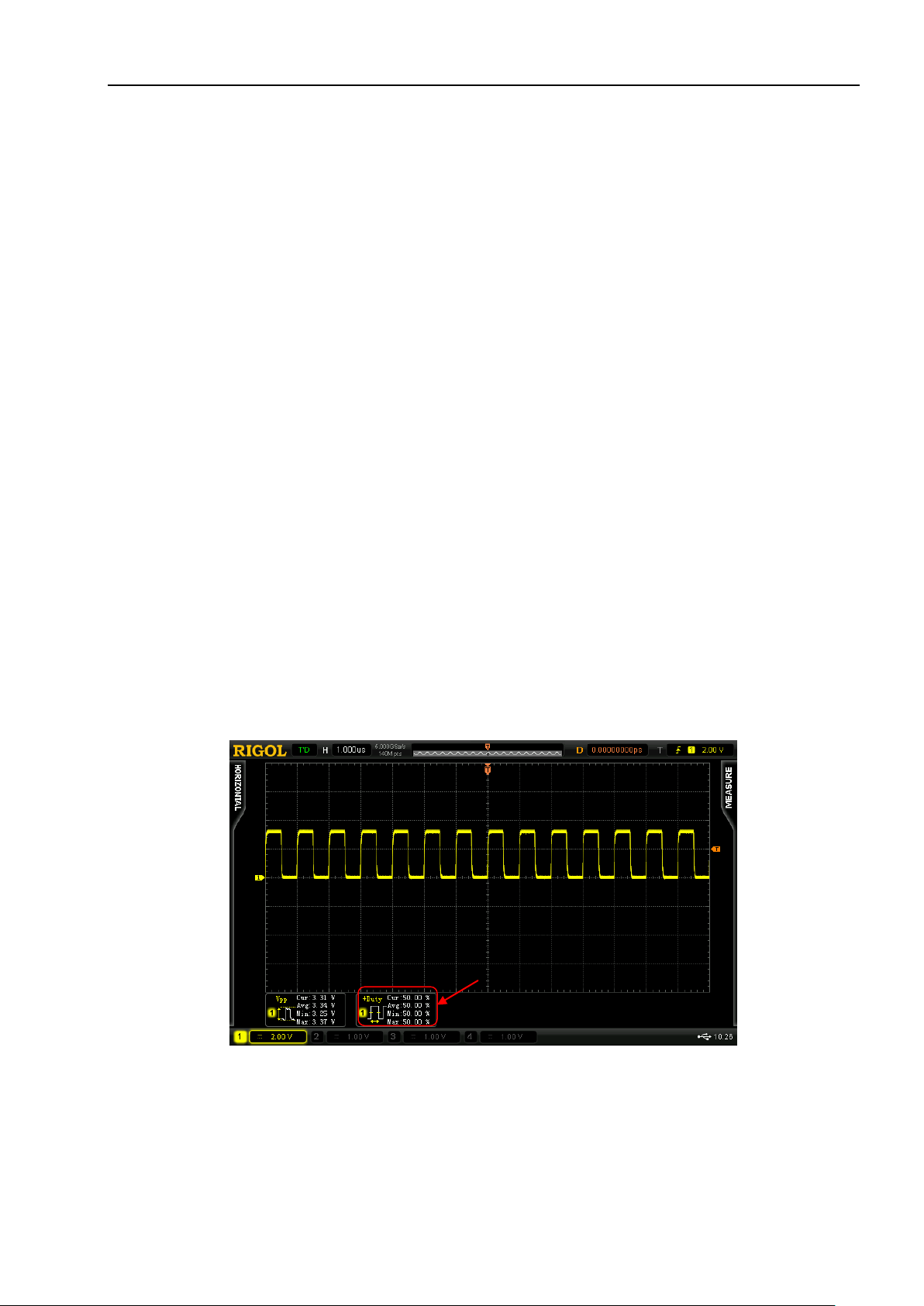
Square waveform with 1MHz frequency, 3.3Vpp amplitude and 50% duty cycle.
2. Functions
Basic signal, edge trigger, duty cycle measurement
3. Demonstration and Result
Connect the signal output pin SQUARE and GND to CH1 of the oscilloscope properly using the
probe;
Set the trigger type to “Edge”, the trigger mode to “Auto” and the vertical scale to “2 V”; adjust
the vertical position and trigger level to appropriate values to make the oscilloscope trigger
stably; enable “+Duty” and “Vpp” measurements and enable statistic function. The
demonstration result is as shown in the figure below.
Figure 3-1 Demonstration Result of Square Waveform
Find Quality Products Online at: [email protected]
User’s Guide for DS6000 Demo Board 3-1
www.GlobalTestSupply.com
Page 12
RIGOL Chapter 3 Demo Board Applications
3-2
3.1.2 Sine Signal
1. Signal Explanation
Signal Output Pin: SINE
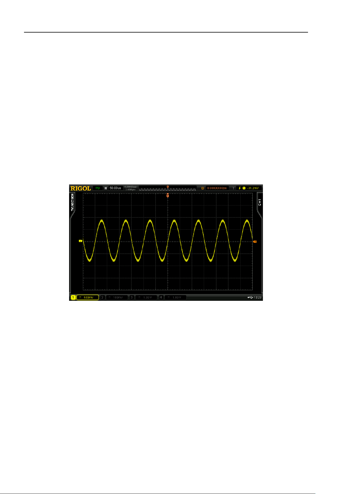
Sine signal with 500 KHz frequency and 1 Vpp amplitude.
2. Functions
Basic signal, edge trigger, FFT
3. Demonstration and Result
Connect the signal output pin SINE and GND to CH1 of the oscilloscope properly using the
probe;
Set the trigger type to “Edge”, the trigger mode to “Auto” and the vertical scale to “500 mV”;
adjust the vertical position and trigger level to appropriate values to make the oscilloscope
trigger stably. The demonstration result is as shown in the figure below.
Figure 3-2 Demonstration Result of Sine Signal
Find Quality Products Online at: [email protected]
www.GlobalTestSupply.com
User’s Guide for DS6000 Demo Board
Page 13
Chapter 3 Demo Board Applications RIGOL
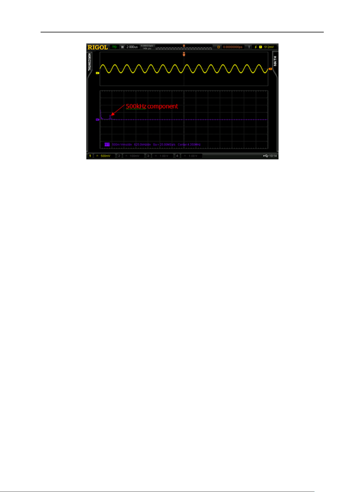
Enable “FFT” operation and the signal frequency is 500 kHz as shown in the figure below.
Figure 3-3 FFT Operation Result of Sine Signal
Find Quality Products Online at: [email protected]
User’s Guide for DS6000 Demo Board 3-3
www.GlobalTestSupply.com
Page 14
RIGOL Chapter 3 Demo Board Applications
3-4
DAC_IN7
DAC_IN6
DAC_IN5
DAC_IN4
DAC_IN3
DAC_IN2
DAC_IN1
DAC_IN0
3.1.3 DA Output Signal
1. Signal Explanation
Signal Output Pin:
UF_DAC (output the converted and unfiltered sine waveform)
DAC_OUT (output the converted and filtered sine waveform)
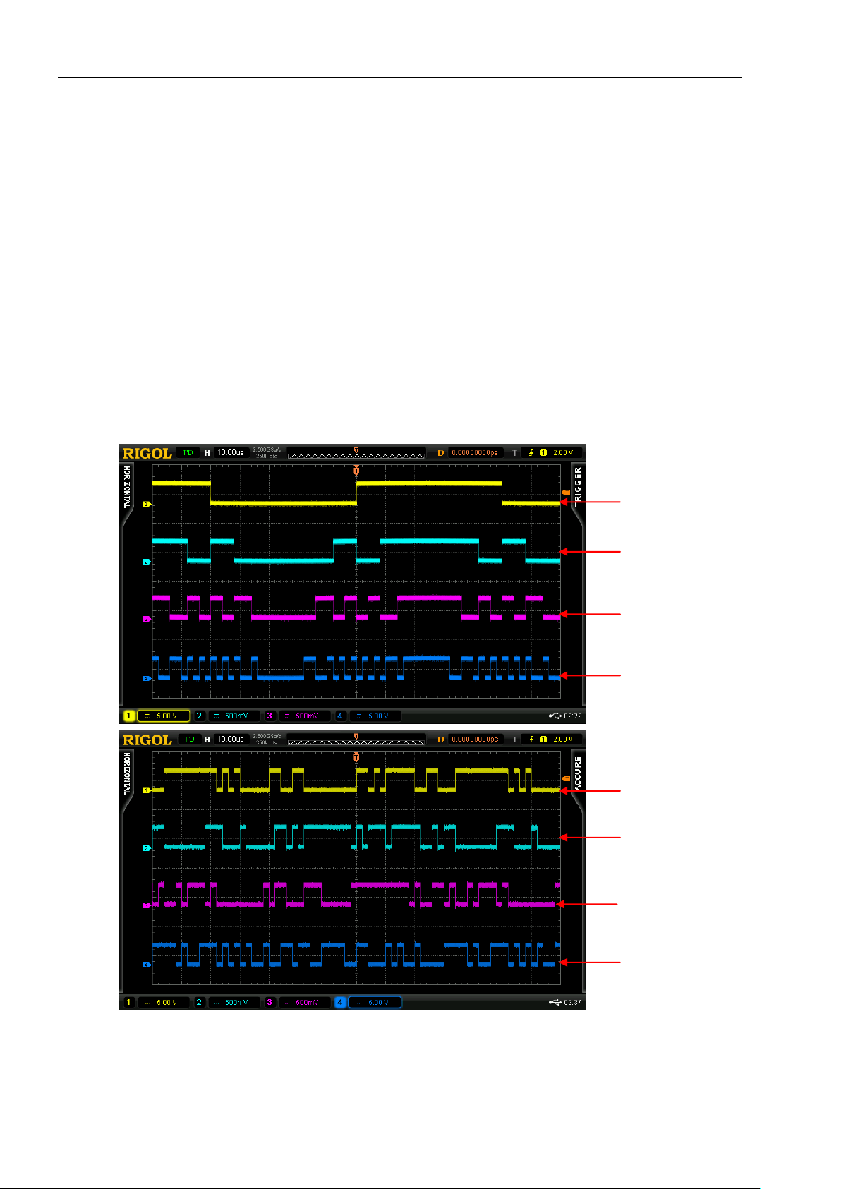
The input of DA conversion are 8 bits, 10kHz digital signals (the signal pins are DAC IN7 to DAC
IN0)
The sample frequency is 25MHz.
2. Functions
MSO, Digital-Analog conversion
3. Demonstration and Result
The digital input signals are as shown in the figures below:
Note: in the figure above, the probe ratio of CH1 and CH4 is “×10”.
Figure 3-4 Digital Input Signals
Find Quality Products Online at: [email protected]
www.GlobalTestSupply.com
User’s Guide for DS6000 Demo Board
Page 15
Chapter 3 Demo Board Applications RIGOL
Unfiltered Sine
Waveform
Filtered Sine
Waveform
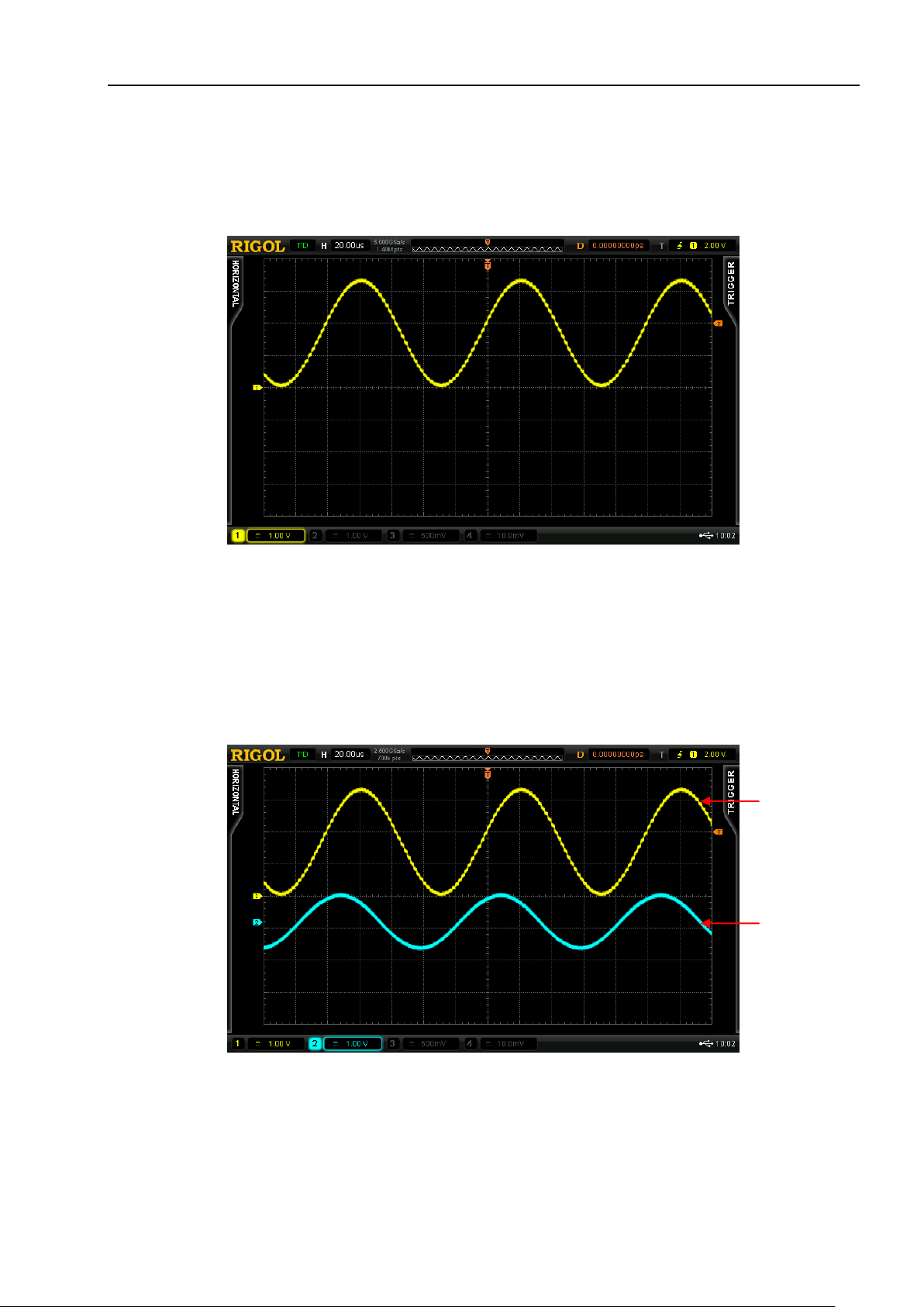
Connect the signal output pin UF_DAC and GND to CH1 of the oscilloscope properly using the
probe;
Set the trigger type to “Edge”, the trigger mode to “Auto” and the vertical scale to “1V”; adjust
the vertical position and trigger level to appropriate values to make the oscilloscope trigger
stably. The analog signal is as shown in the figure below. This signal is the converted and
unfiltered analog signal and the waveform has apparent “steps” as shown in the figure below.
Figure 3-5 Unfiltered Analog Output Signal
Connect the signal output pin DAC_OUT and GND to CH2 of the oscilloscope properly using the
probe;
Set the vertical scale to “1V” and adjust the vertical position and trigger level to make the
oscilloscope trigger stably. The analog signal is as shown in the figure below. This signal is the
converted and filtered analog signal and the waveform is relatively smoother as shown in the
figure below.
Figure 3-6 Analog Output Signal
Find Quality Products Online at: [email protected]
User’s Guide for DS6000 Demo Board 3-5
www.GlobalTestSupply.com
Page 16
RIGOL Chapter 3 Demo Board Applications
3-6
3.1.4 Differential Signal
1. Signal Explanation
Signal Output Pin: DIFF_SIG_N, DIFF_SIG_P
Output 25 MHz random sequence and the level logic is low-voltage differential signal (LVDs).
2. Functions
Differential probe measurement, rising/falling edge trigger, MATH function
3. Demonstration and Result
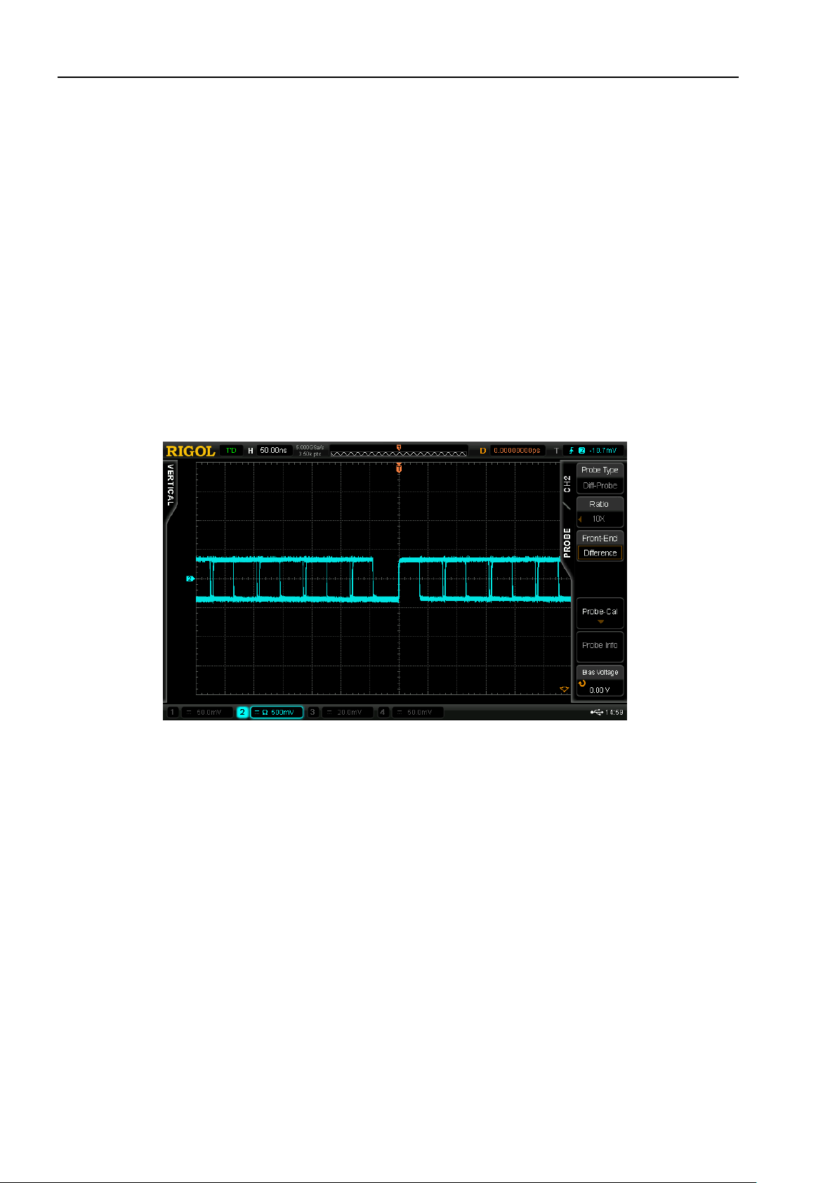
Connect DIFF_SIG_P and DIFF_SIG_N with CH2 using differential probe and the oscilloscope
identifies the differential probe automatically. Set the “Probe Type” to “Diff-Probe”. Set the
trigger type to “Edge”, the trigger mode to “Auto” and the vertical scale to “500 mV”; adjust the
vertical position and trigger level to appropriate values to make the oscilloscope trigger stably.
The demonstration result is as shown in the figure below.
Figure 3-7 Differential Signal Measurement Using Differential Probe
Find Quality Products Online at: [email protected]
www.GlobalTestSupply.com
User’s Guide for DS6000 Demo Board
Page 17
Chapter 3 Demo Board Applications RIGOL
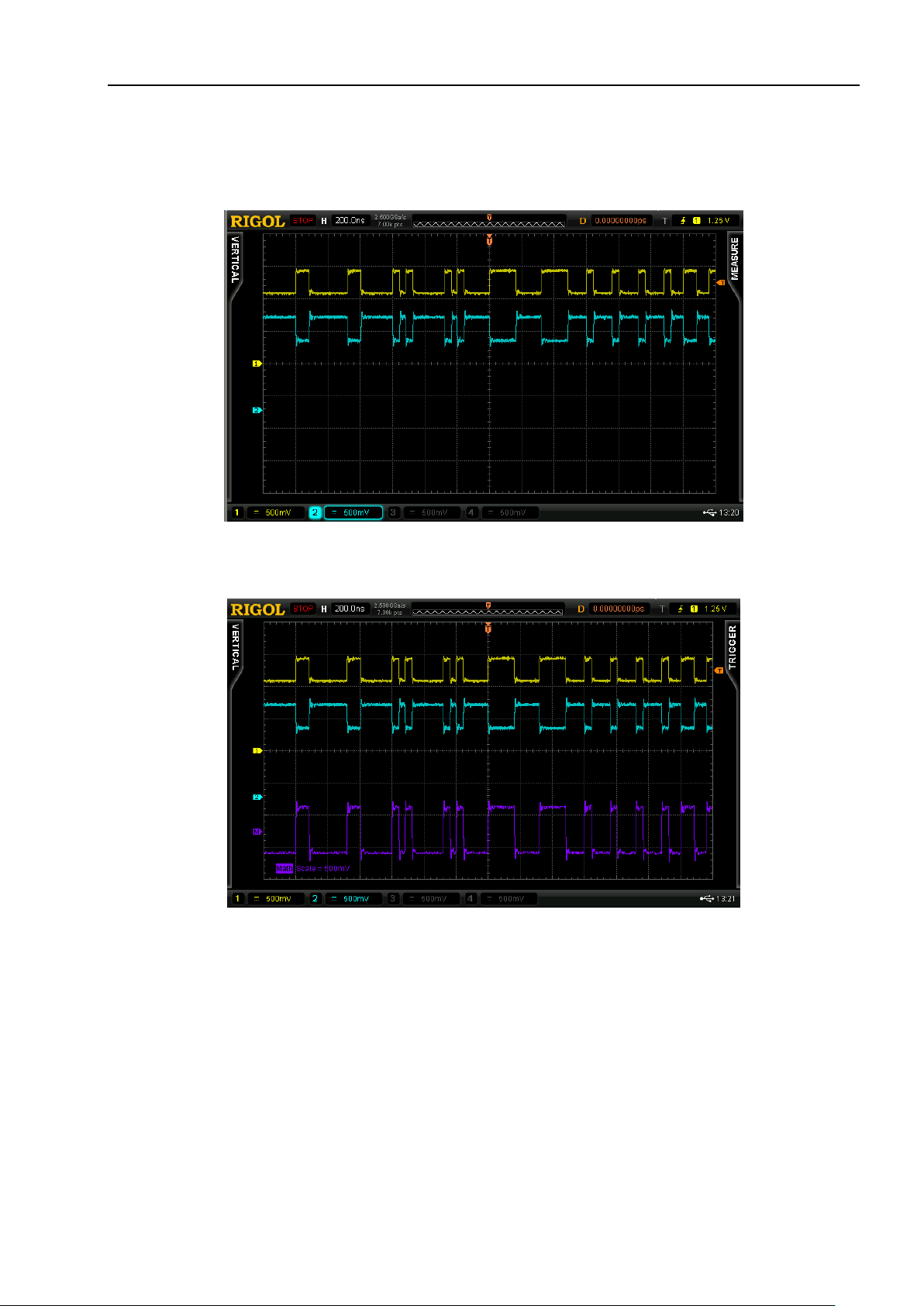
Connect DIFF_SIG_P and GND to CH1 of the oscilloscope using single-ended probe;
Connect DIFF_SIG_N and GND to CH2 of the oscilloscope using single-ended probe;
Set the trigger type to “Edge”, the trigger mode to “Single” and the vertical scale to “500 mV”;
adjust the vertical position and trigger level to appropriate values to make the oscilloscope
trigger stably. The demonstration result is as shown in the figure below.
Figure 3-8 Differential signal Demonstration Using Single-ended Probe
Enable MATH function (A-B). Set source A to CH1 and source B to CH2. The operation result is as
shown in the figure below.
Figure 3-9 MATH Function Demonstration Using Single-ended Probe
Find Quality Products Online at: [email protected]
User’s Guide for DS6000 Demo Board 3-7
www.GlobalTestSupply.com
Page 18
RIGOL Chapter 3 Demo Board Applications
3-8
3.1.5 PAL Video Signal
1. Signal Explanation
Signal Output Pin: VIDEO_SIGNAL (select PAL)
The signal amplitude is 1Vpp.
2. Functions
Video Trigger
3. Demonstration and Result
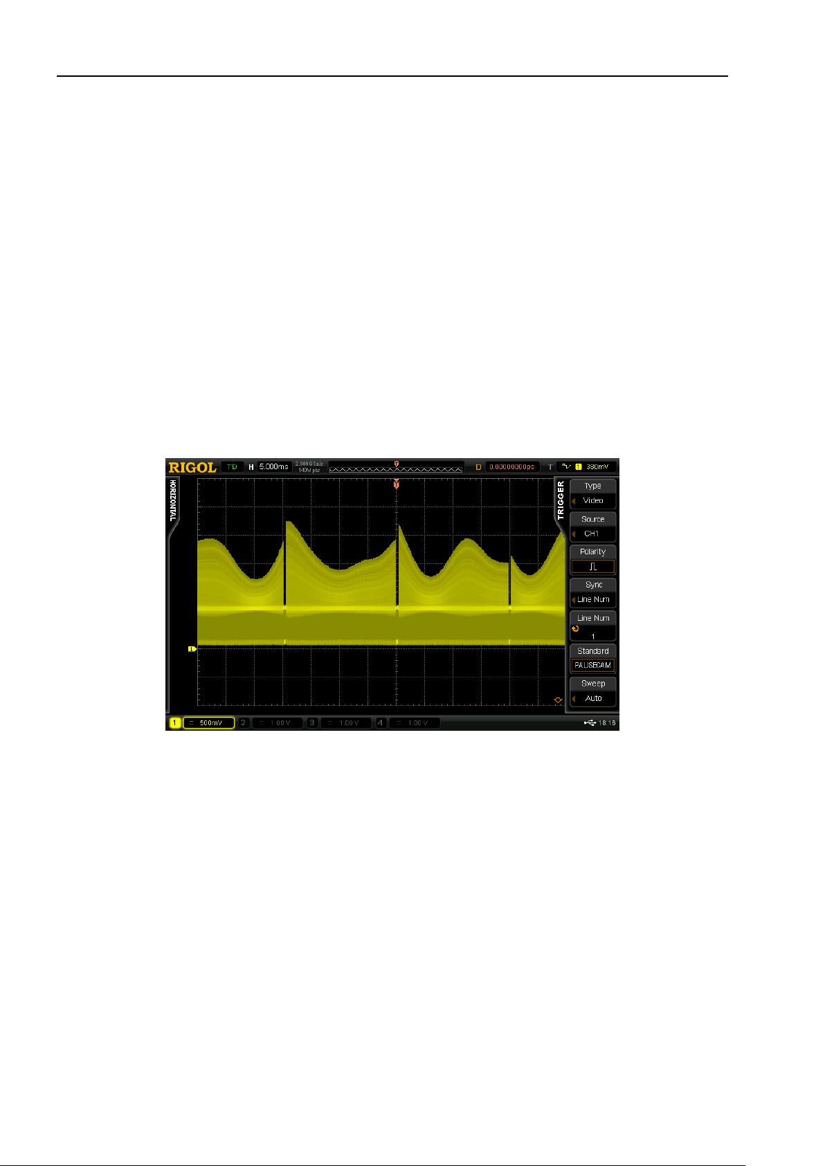
Select PAL from VIDEO MODE of the demo board. Connect the signal output pin VIDEO SIGNAL
and GND to CH1 of the oscilloscope properly using the probe;
Set the trigger type to “Video”, the video standard to “PAL/SECAM”, the video polarity to
“Positive”, the synchronization to “Line number”, the line number to “1” and the vertical scale to
“500 mV”; adjust the vertical position and trigger level to appropriate values to make the
oscilloscope trigger stably. The demonstration result is as shown in the figure below.
Figure 3-10 PAL Video Signal
Find Quality Products Online at: [email protected]
www.GlobalTestSupply.com
User’s Guide for DS6000 Demo Board
Page 19
Chapter 3 Demo Board Applications RIGOL
3.1.6 NTSC Video Signal
1. Signal Explanation
Signal Output Pin: VIDEO_SIGNAL (select NTSC)
The signal amplitude is 1Vpp.
2. Functions
Video trigger
3. Demonstration and Result
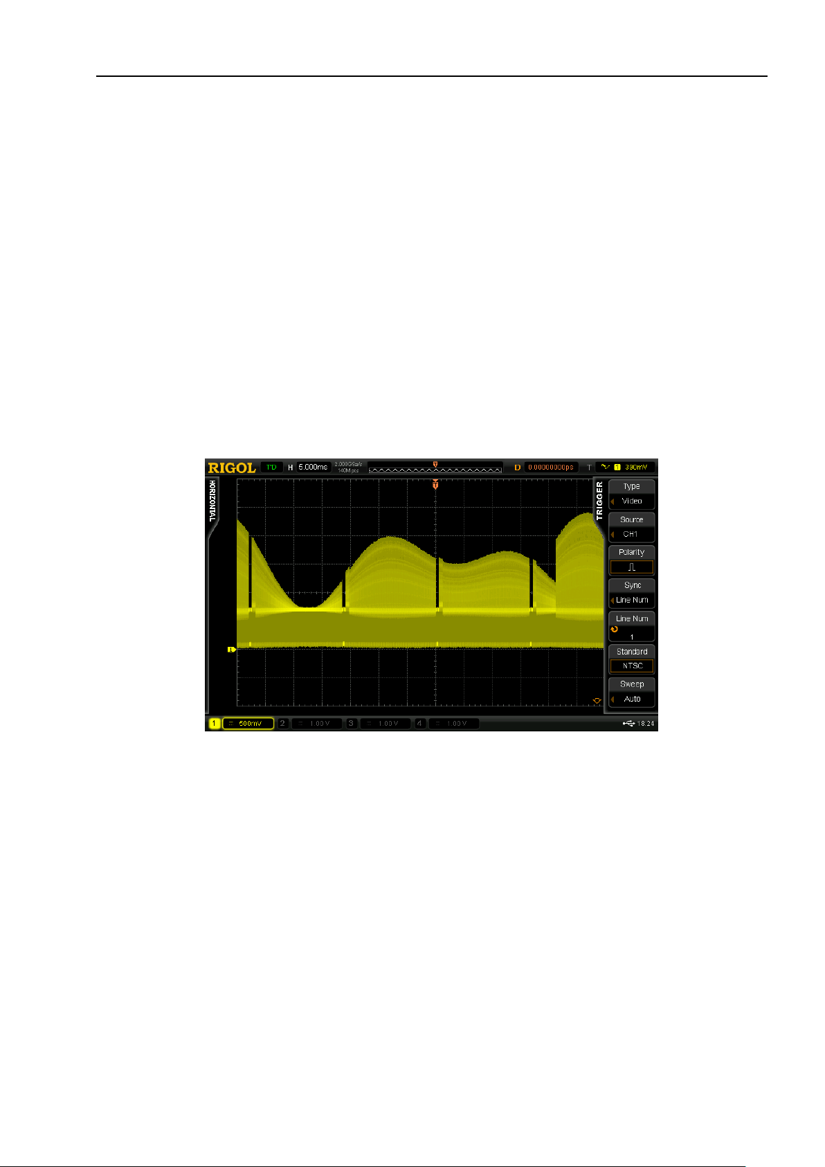
Select NTSC from VIDEO MODE of the demo board. Connect the signal output pin VIDEO
SIGNAL and GND to CH1 of the oscilloscope properly using the probe;
Set the trigger type to “Video”, the video standard to “NTSC”, the video polarity to “Positive”, the
synchronization to “Line number”, the line number to “1” and the vertical scale to “500 mV”;
adjust the vertical position and trigger level to appropriate values to make the oscilloscope
trigger stably. The demonstration result is as shown in the figure below.
Figure 3-11 NTSC Video Signal
Find Quality Products Online at: [email protected]
User’s Guide for DS6000 Demo Board 3-9
www.GlobalTestSupply.com
Page 20
RIGOL Chapter 3 Demo Board Applications
3-10
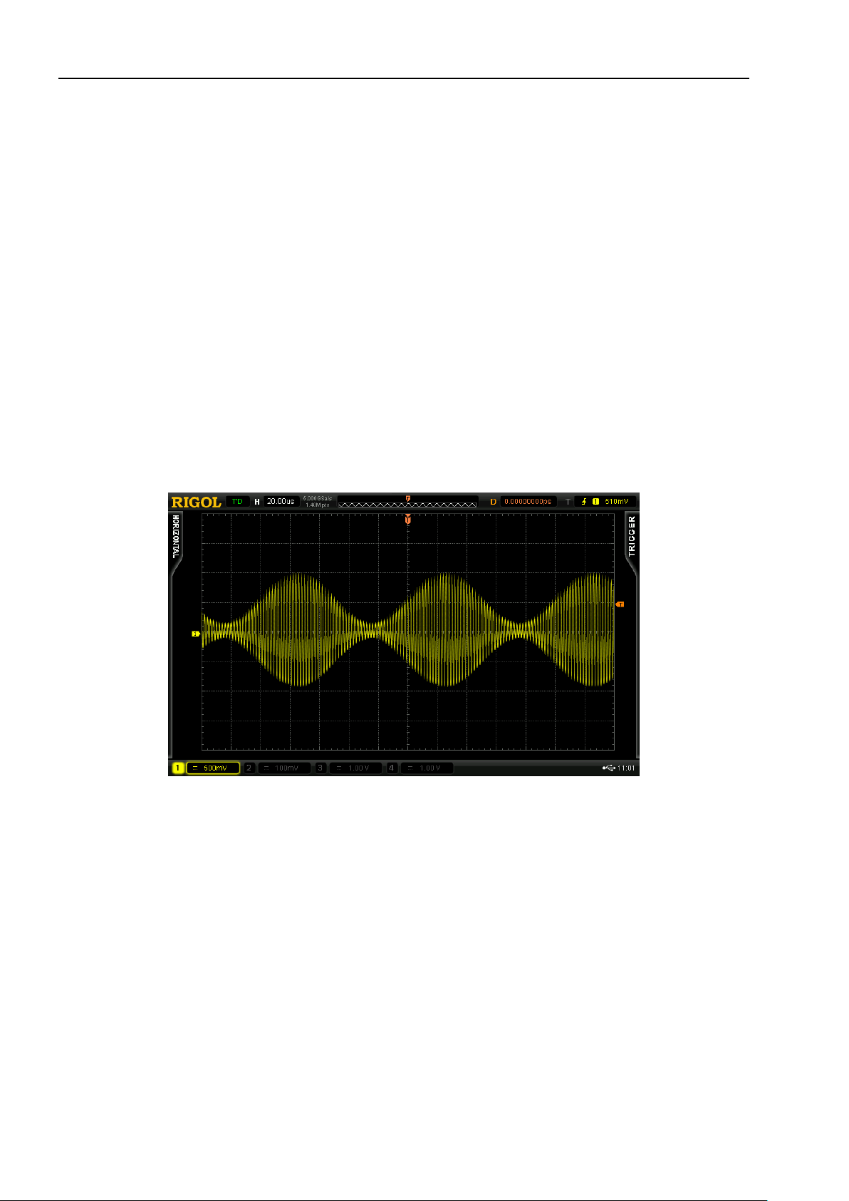
3.1.7 Amplitude Modulation Signal
1. Signal Explanation
Signal Output Pin: AM_MOD
Carrier waveform: 500kHz, 1Vpp sine waveform;
Modulating waveform: 10kHz, 1.6Vpp sine waveform.
2. Functions
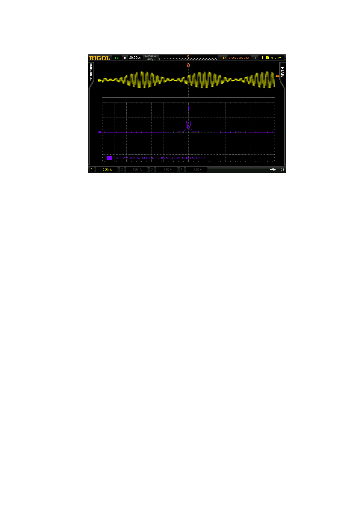
Trigger holdoff, FFT
3. Demonstration and Result
Connect the signal output pin AM_MOD and GND to CH1 of the oscilloscope properly using the
probe;
Set the trigger type to “Edge”, the trigger mode to “Auto”, the trigger holdoff to “70us” and the
acquisition mode to “Normal”; adjust the vertical position and trigger level to appropriate values
to make the oscilloscope trigger stably. The demonstration result is as shown in the figure
below.
Figure 3-12 Amplitude Modulation Signal
Find Quality Products Online at: [email protected]
www.GlobalTestSupply.com
User’s Guide for DS6000 Demo Board
Page 21
Chapter 3 Demo Board Applications RIGOL
Enable FFT operation function. Set the vertical scale to 100mVrms/div and the center frequency
to 500 KHz. The operation result is as shown in the figure below.
Figure 3-13 FFT Operation Result of Amplitude Modulation Signal
Find Quality Products Online at: [email protected]
User’s Guide for DS6000 Demo Board 3-11
www.GlobalTestSupply.com
Page 22
RIGOL Chapter 3 Demo Board Applications
3-12
3.2 Special Signal Applications
3.2.1 Noisy Sine Signal
1. Signal Explanation
Signal Output Pin: NOISY_SINE
500 kHz, 1Vpp sine waveform on which a 25MHz, 300mVpp high-frequency noise is
superimposed.
2. Functions
High-frequency reject, bandwidth limit, FFT
3. Demonstration and Result
Connect the signal output pin NOISY_SINE and GND to CH1 of the oscilloscope properly using
the probe;
Set the trigger type to “Edge”, the trigger holdoff to “600us”, the sample mode to “Normal” and
the vertical scale to “500 mV”; adjust the vertical position and trigger level to appropriate values
to make the oscilloscope trigger stably. The demonstration result is as shown in the figure
below.
Figure 3-14 Sine Signal Superimposed with Noise
Find Quality Products Online at: [email protected]
www.GlobalTestSupply.com
User’s Guide for DS6000 Demo Board
Page 23
Chapter 3 Demo Board Applications RIGOL
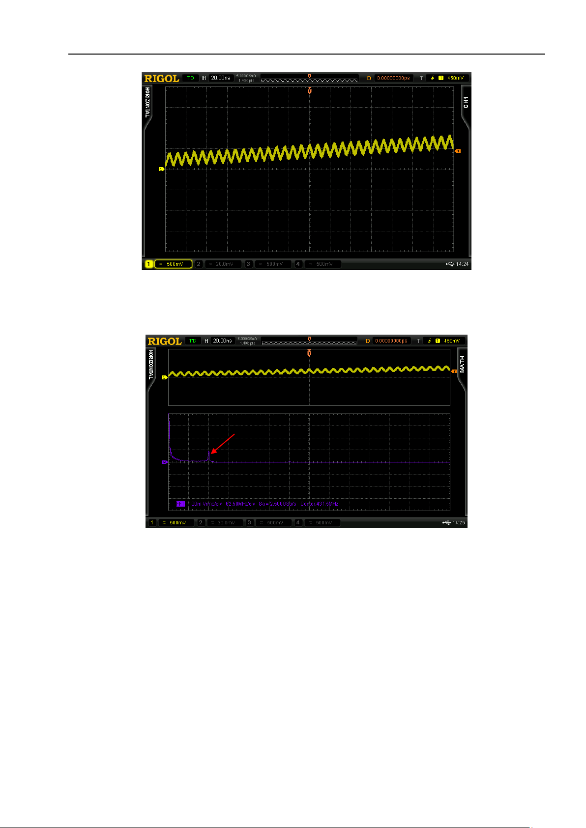
125MHz noise component
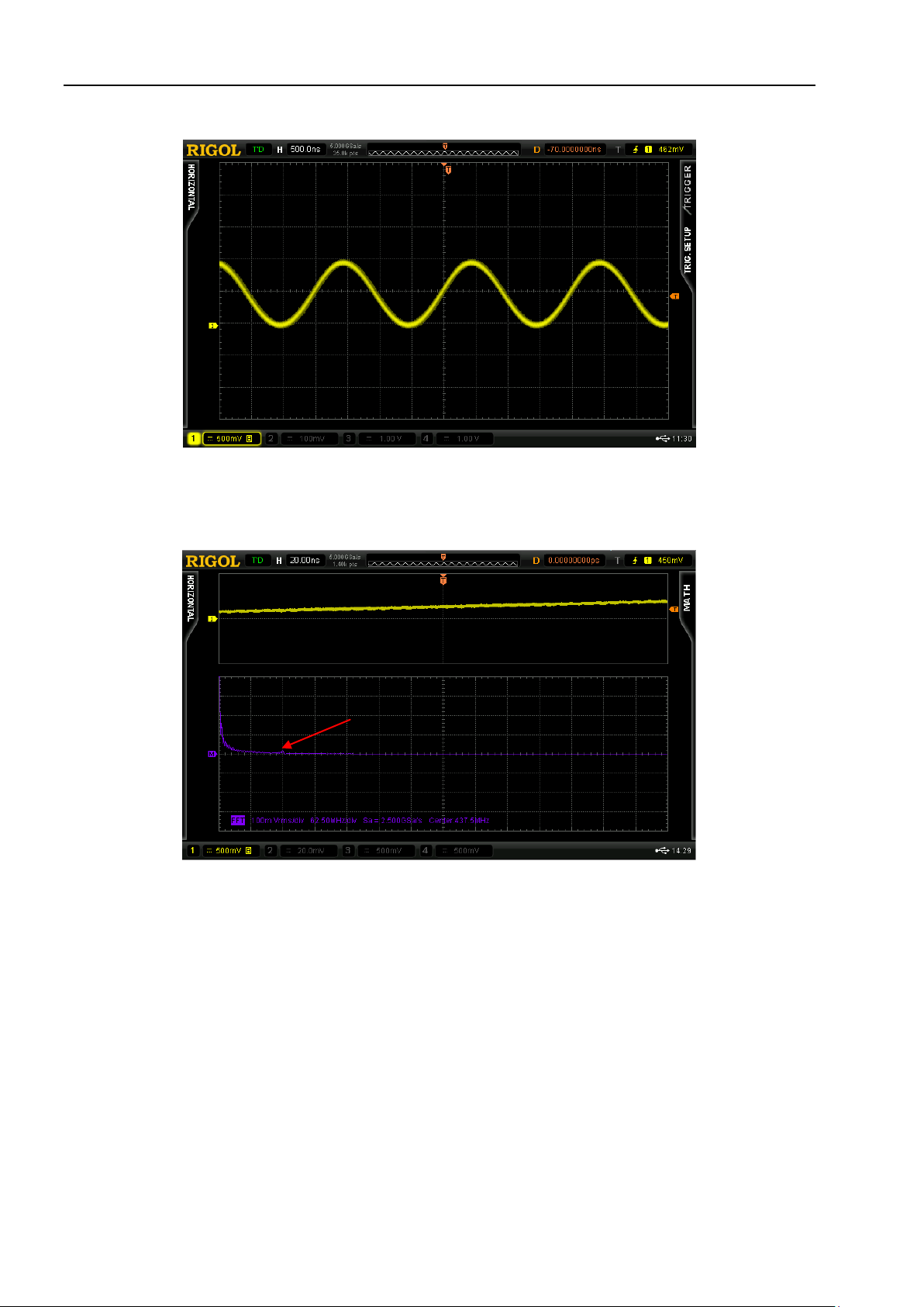
Adjust the horizontal time base to “20 ns” and the waveform is as shown in the figure below.
Figure 3-15 High-frequency Noise Details
Enable FFT operation. Set the signal source to “CH1”, the window function to “Rectangle”, the
vertical scale unit to “Vrms”, the vertical scale to “100 mVrms” and the horizontal scale to
“62.5MHz”. The operation result is as shown in the figure below.
Figure 3-16 FFT Operation Result of Noisy Sine Signal
Find Quality Products Online at: [email protected]
User’s Guide for DS6000 Demo Board 3-13
www.GlobalTestSupply.com
Page 24
RIGOL Chapter 3 Demo Board Applications
3-14
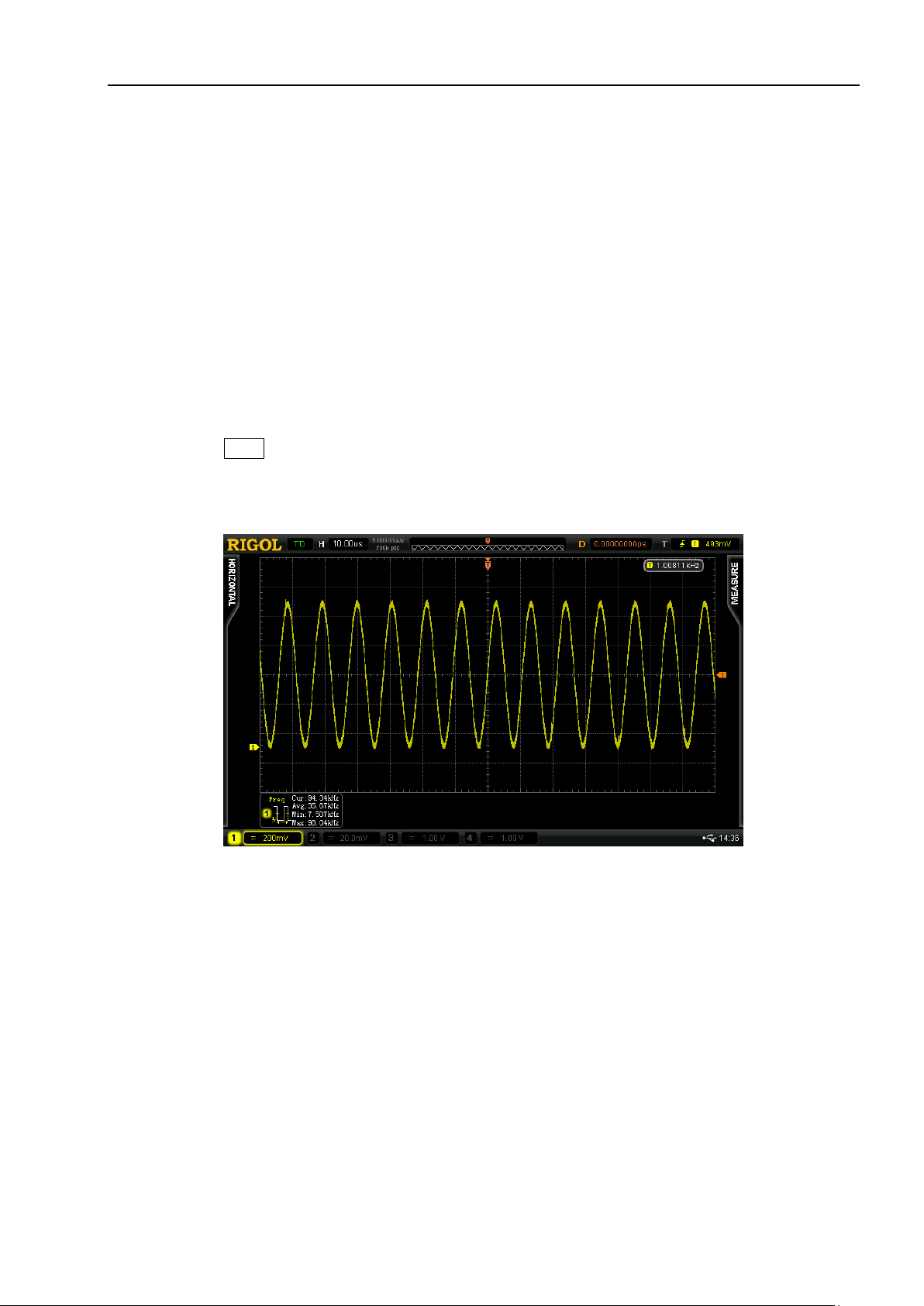
The noise component is basically rejected
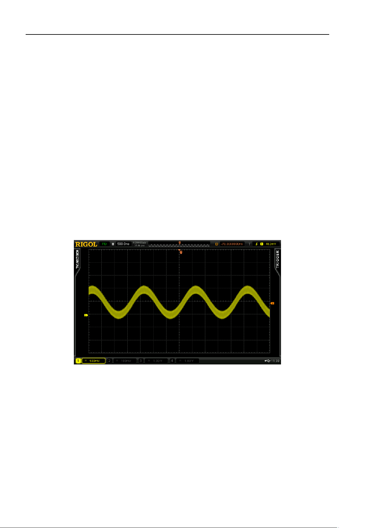
Disable FFT operation, adjust the horizontal time base to “500 ns” and enable “HF Reject” and
“Bandwidth Limit”. The demonstration result is as shown in the figure below.
Figure 3-17 Signal after Noise Reject
Adjust the horizontal time base to “20ns” again. Enable FFT operation and set the related
parameters as above. The operation result is as shown in the figure below (the noise component
is basically rejected).
Figure 3-18 FFT Operation Result after Noise Reject
Find Quality Products Online at: [email protected]
www.GlobalTestSupply.com
User’s Guide for DS6000 Demo Board
Page 25
Chapter 3 Demo Board Applications RIGOL
3.2.2 Slow Sweep Signal
1. Signal Explanation
Signal Output Pin: SWEEP (select SLOW)
The frequency range of the sweep is from 1kHz to 100kHz, the sweep time is 40s and the sweep
mode is log.
2. Functions
Measurement statistic, persistence display
3. Demonstration and Result
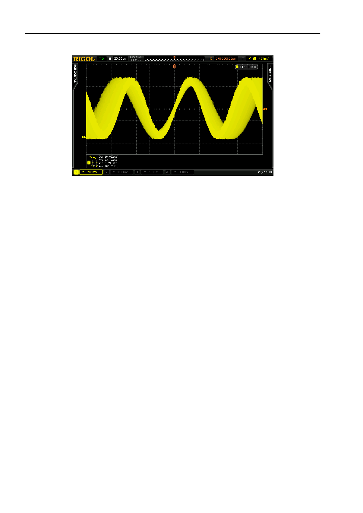
Set the “SWEEP MODE” to “SLOW” from the demo board; connect the signal output pin SWEEP
to the oscilloscope properly using the probe.
Press Auto at the front panel of the oscilloscope to set the oscilloscope parameters
automatically. Enable frequency measurement and statistic function. Basically, the frequency
range of the sweep can be determined through the maximum and minimum of the statistic
function as shown in the figure below.
Figure 3-19 Slow Sweep Signal
Find Quality Products Online at: [email protected]
User’s Guide for DS6000 Demo Board 3-15
www.GlobalTestSupply.com
Page 26
RIGOL Chapter 3 Demo Board Applications
3-16
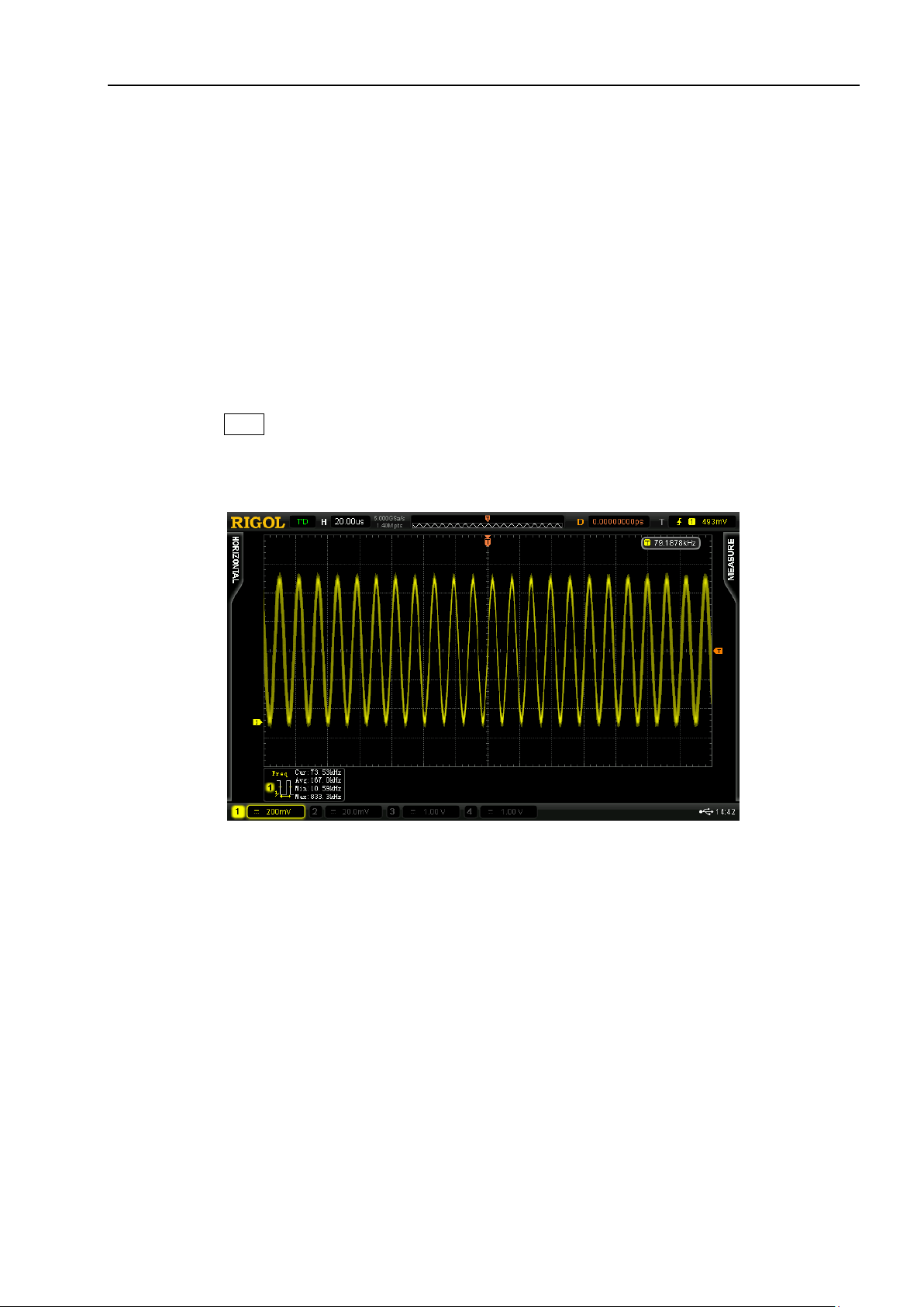
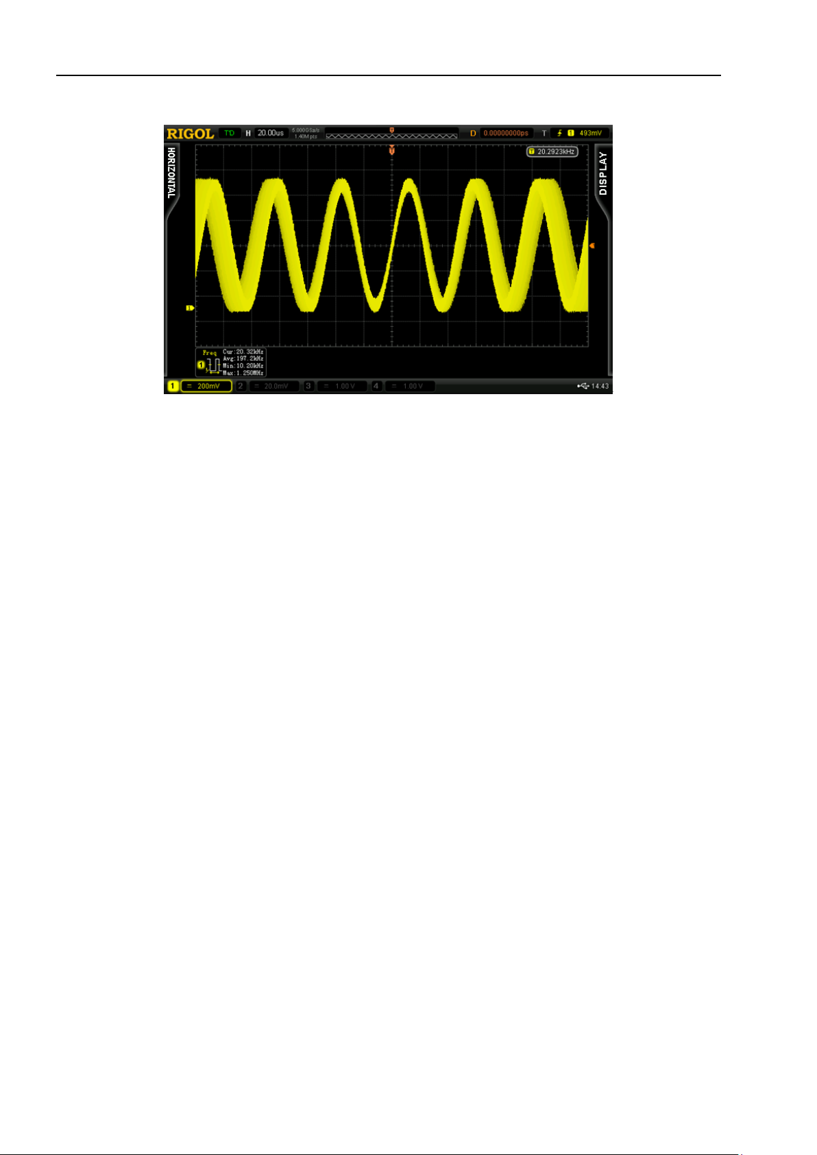
Adjust the “Persistence Time” to 20s and the sweep trace of the sweep signal is clearly displayed
as shown in the figure below.
Figure 3-20 Sweep Trace of the Slow Sweep Signal
Find Quality Products Online at: [email protected]
www.GlobalTestSupply.com
User’s Guide for DS6000 Demo Board
Page 27
Chapter 3 Demo Board Applications RIGOL
3.2.3 Fast Sweep Signal
1. Signal Explanation
Signal Output Pin: SWEEP (FAST)
The frequency range of the sweep is from 10kHz to 1MHz and the sweep time is 8s.
2. Functions
Measurement statistic, persistence display
3. Demonstration and Result
Set the “SWEEP MODE” to “FAST” from the demo board; connect the signal output pin SWEEP
and GND to the oscilloscope properly.
Press Auto at the front panel of the oscilloscope to set the oscilloscope parameters
automatically. Enable frequency measurement and statistic function. Basically, the frequency
range of the sweep can be determined through the maximum and minimum in the statistic
function as shown in the figure below.
Figure 3-21 Fast Sweep Signal
Find Quality Products Online at: [email protected]
User’s Guide for DS6000 Demo Board 3-17
www.GlobalTestSupply.com
Page 28
RIGOL Chapter 3 Demo Board Applications
3-18
Adjust the “Persistence Time” to 500ms and the sweep trace of the sweep signal is clearly
displayed.
Figure 3-22 Sweep Trace of the Fast Sweep Signal
Find Quality Products Online at: [email protected]
www.GlobalTestSupply.com
User’s Guide for DS6000 Demo Board
Page 29
Chapter 3 Demo Board Applications RIGOL
3.2.4 Phase Deviation Signal
1. Signal Explanation
Signal Output Pin: CLOCK, DELAY_CLOCK
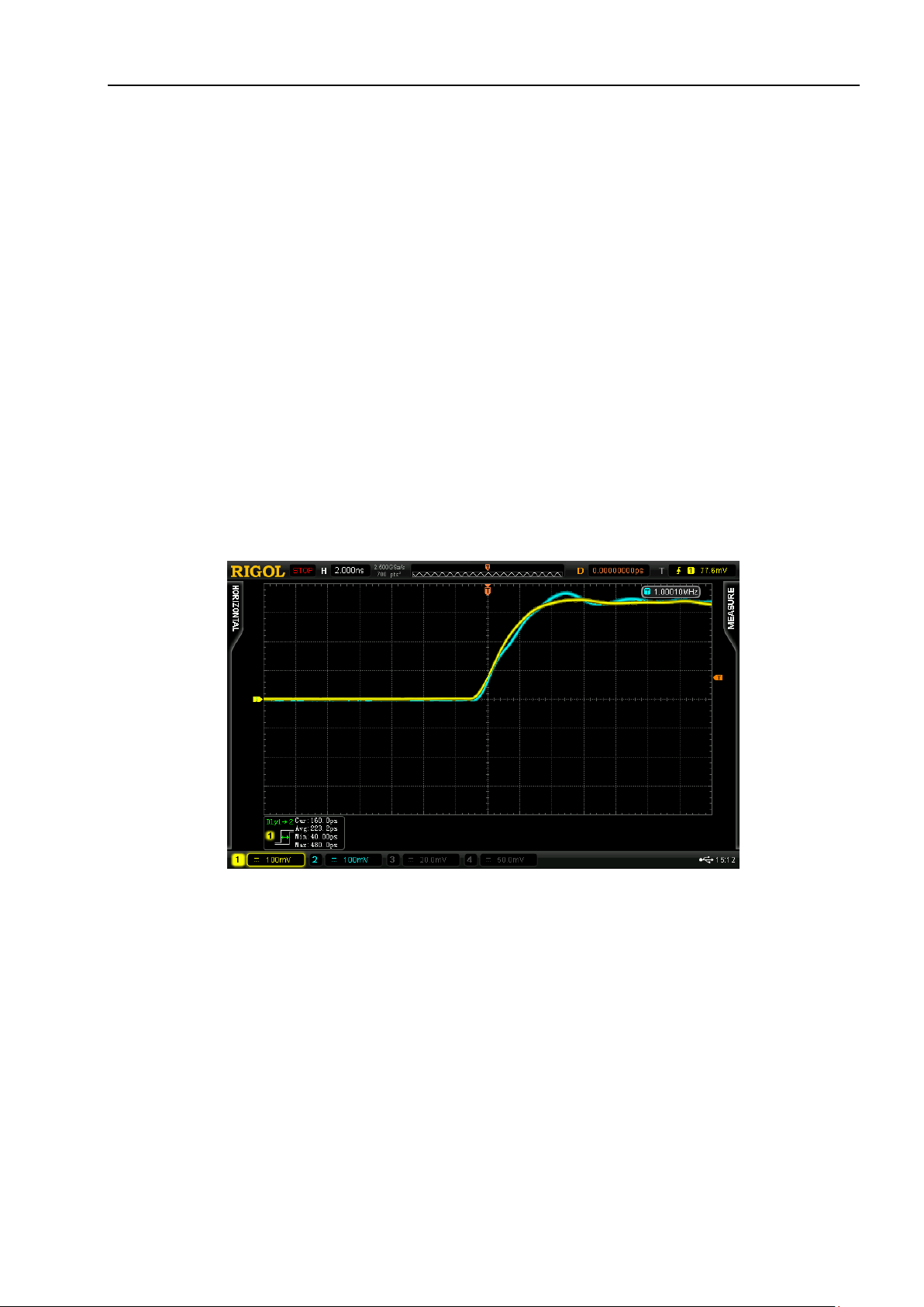
The clock frequency is 1 MHz and the delay time cannot exceed 4ns.
2. Functions
Channel delay measurement
3. Demonstration and Result
Connect CLOCK and GND to CH1 of the oscilloscope using the probe; enable CH1, set the
vertical scale to “100 mV”, the vertical position to “0”, the trigger type to “Edge”, the trigger
source to “CH1”, the edge type to “Leading” and the trigger mode to “Auto”; adjust the trigger
level to an appropriate value to make the oscilloscope trigger stably.
Connect DELAY_CLOCK and GND to CH2 the probe; enable CH2, set the vertical scale to “100
mV” and vertical position to “0”.
Enable delay measurement of the rising edge as well as statistic function. The demonstration
result is as shown in the figure below.
Figure 3-23 Channel Delay Measurement
Find Quality Products Online at: [email protected]
User’s Guide for DS6000 Demo Board 3-19
www.GlobalTestSupply.com
Page 30
RIGOL Chapter 3 Demo Board Applications
3-20
Rare Abnormal Signal
3.2.5 Rare Abnormal Signal
1. Signal Explanation
Signal Output Pin: RARE_AN
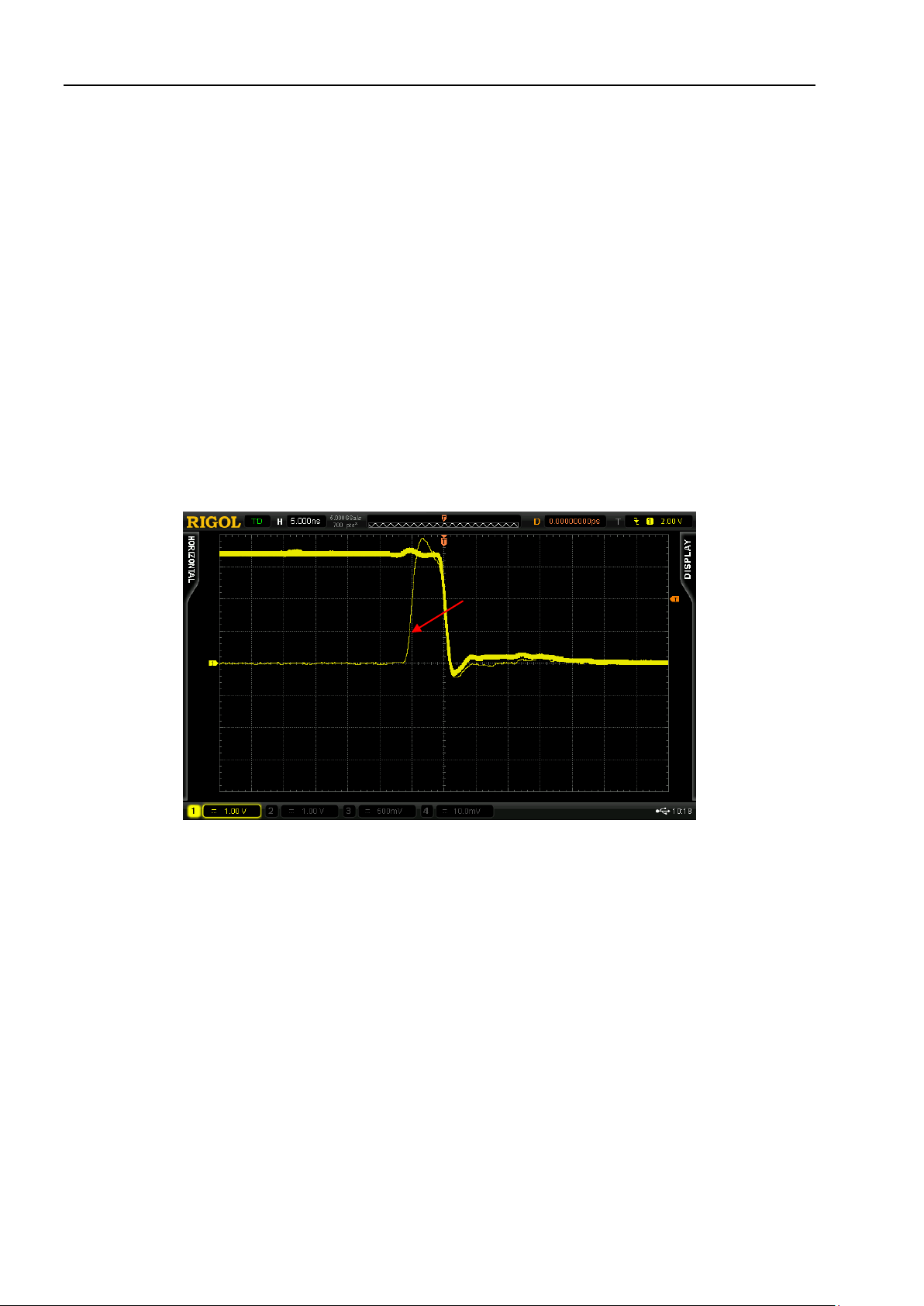
Square waveform with 1MHz frequency. Narrow pulse occurs every 100ms and the pulse width
cannot exceed 5ns.
2. Functions
Waveform capture rate, waveform record and analysis
3. Demonstration and Result
Connect the signal output pin RARE_AN and GND to CH1 of the oscilloscope properly using the
probe;
Set the trigger type to “Edge”, the trigger mode to “Single”, the horizontal time base to 5ns, the
waveform capture rate to 180kHz, the memory depth to “Auto”. Set the persistence time to 20s
and the capture result of abnormal signal is as shown in the figure below.
Figure 3-24 Rare Abnormal Signal
Find Quality Products Online at: [email protected]
www.GlobalTestSupply.com
User’s Guide for DS6000 Demo Board
Page 31
Chapter 3 Demo Board Applications RIGOL
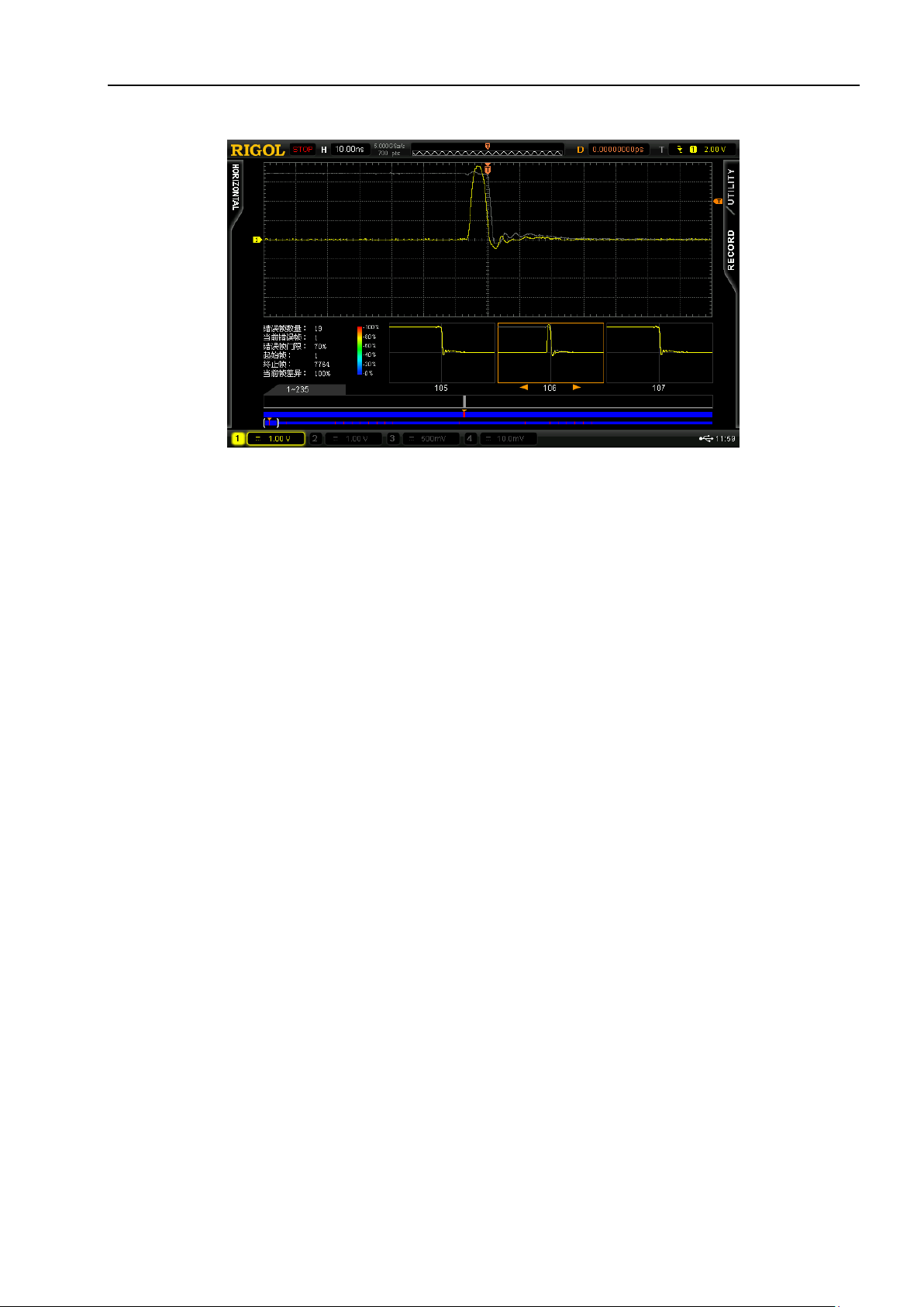
Enable the waveform record function. After the record finishes, use the waveform playback and
analysis function to analyze the accidental pulse.
Figure 3-25 Waveform Record and Analysis
Find Quality Products Online at: [email protected]
User’s Guide for DS6000 Demo Board 3-21
www.GlobalTestSupply.com
Page 32
RIGOL Chapter 3 Demo Board Applications
3-22
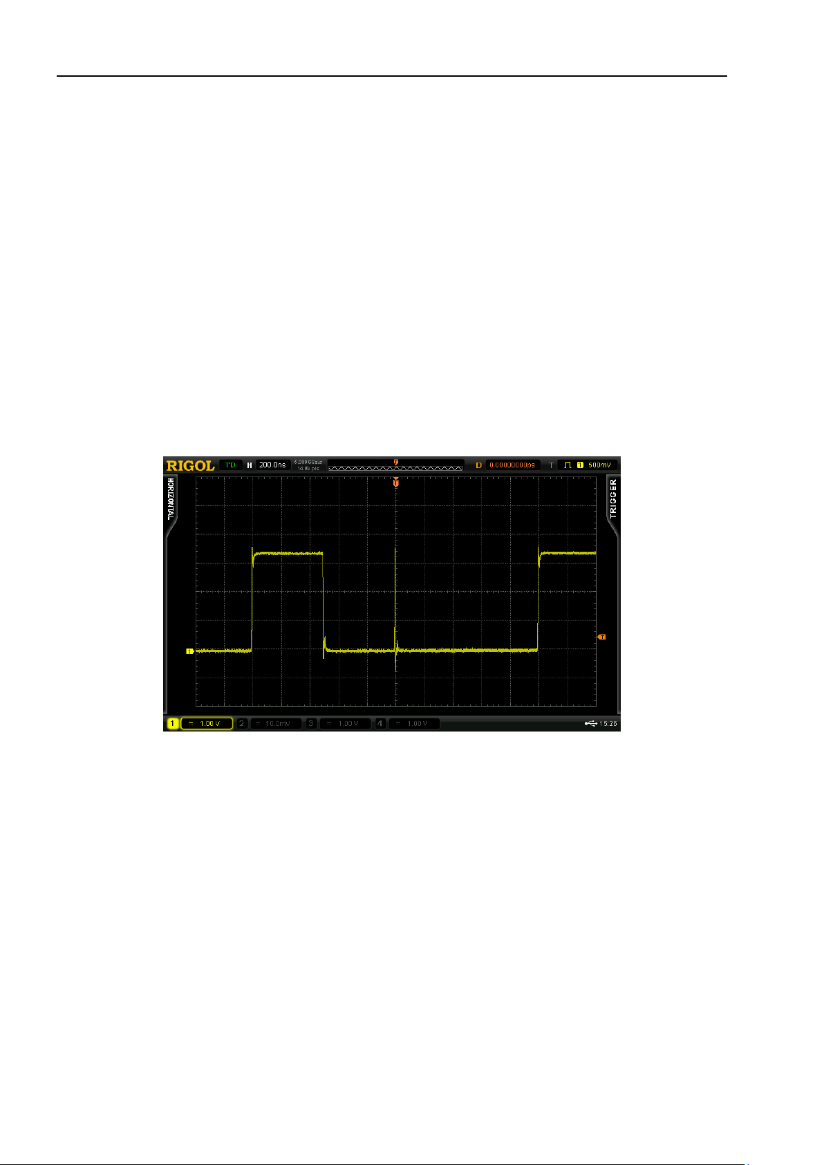
3.2.6 Frequent Abnormal Signal
1. Signal Explanation
Signal Output Pin: FREQ_AN
Square waveform with 1MHz frequency. Narrow pulse occurs every 1ms and the pulse width
cannot exceed 5ns.
2. Functions
Pass/Fail, pulse trigger
3. Demonstration and Result
Connect the signal output pin FREQ_AN and GND to CH1 of the oscilloscope properly using the
probe.
Set the trigger type to “Pulse”, the trigger condition to <6ns the trigger mode to “Auto” and the
trigger level to 500mV. At this point, the abnormal signals can be observed stably as shown in
the figure below.
Figure 3-26 Stable Display of Frequent Abnormal Signal
Find Quality Products Online at: [email protected]
www.GlobalTestSupply.com
User’s Guide for DS6000 Demo Board
Page 33
Chapter 3 Demo Board Applications RIGOL
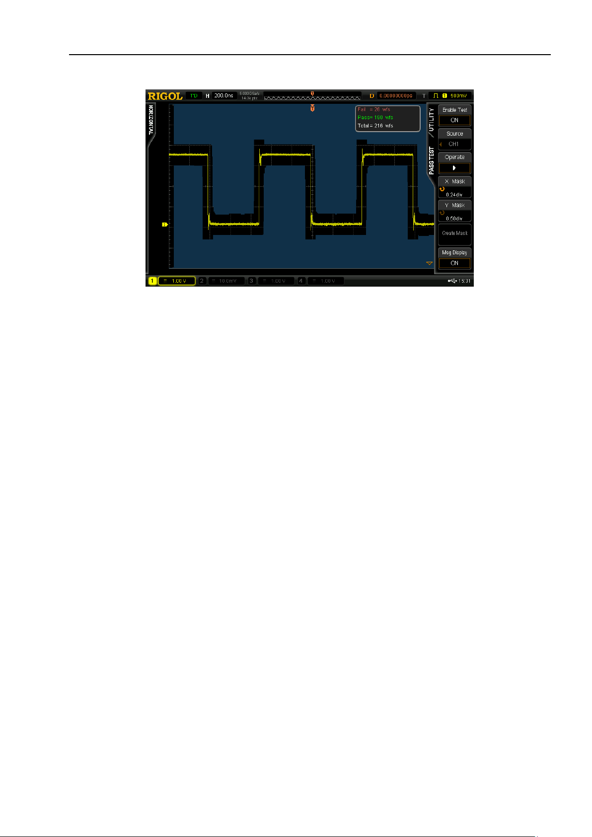
Enable Pass/Fail mode. Set X mask to 0.24div and Y mask to 0.50div. The demonstration result is
as shown in the figure below.
Figure 3-27 Pass/Fail Test of Frequent Abnormal Signal
Find Quality Products Online at: [email protected]
User’s Guide for DS6000 Demo Board 3-23
www.GlobalTestSupply.com
Page 34
RIGOL Chapter 3 Demo Board Applications
3-24
3.2.7 Manual Abnormal Signal
1. Signal Explanation
Signal Output Pin: MANU_AN
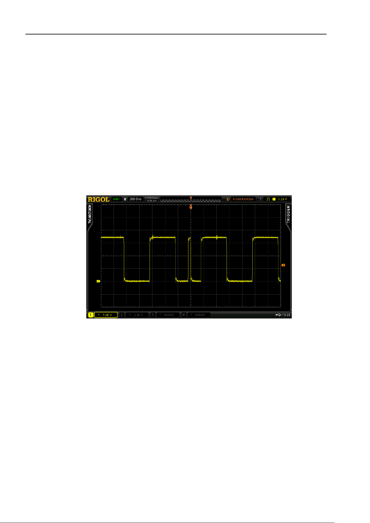
Square waveform with 1.25MHz frequency. Narrow pulse with 40ns pulse width is output every
time the key is pressed.
2. Functions
Pulse trigger
3. Demonstration and Result
Connect the signal output pin MANU_AN to CH1 of the oscilloscope properly using the probe.
Set the trigger type to “Pulse”, the trigger condition to <40ns, the trigger mode to “Normal” and
the vertical scale to “1 V”; adjust the vertical position and trigger level to appropriate values. The
demonstration result is as shown in the figure below.
Figure 3-28 Manual Abnormal Signal
Find Quality Products Online at: [email protected]
www.GlobalTestSupply.com
User’s Guide for DS6000 Demo Board
Page 35
Chapter 3 Demo Board Applications RIGOL
3.2.8 Manual Burst Signal
1. Signal Explanation
Signal Output Pin: MANU_BST
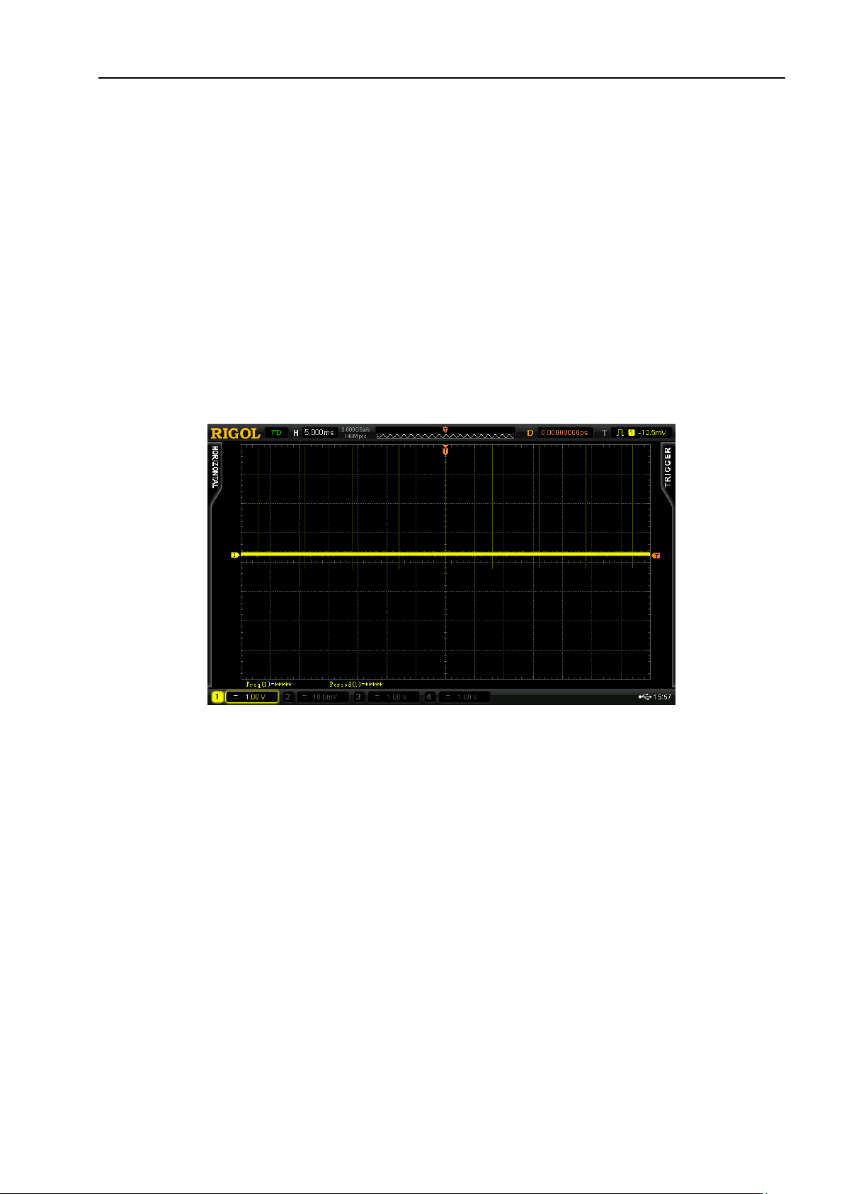
25 bursts. Each burst contains high level and low level.
2. Functions
Pulse trigger, high sample rate, deep memory
3. Demonstration and Result
Connect the signal output pin MANU_BST and GND to CH1 of the oscilloscope properly using the
probe.
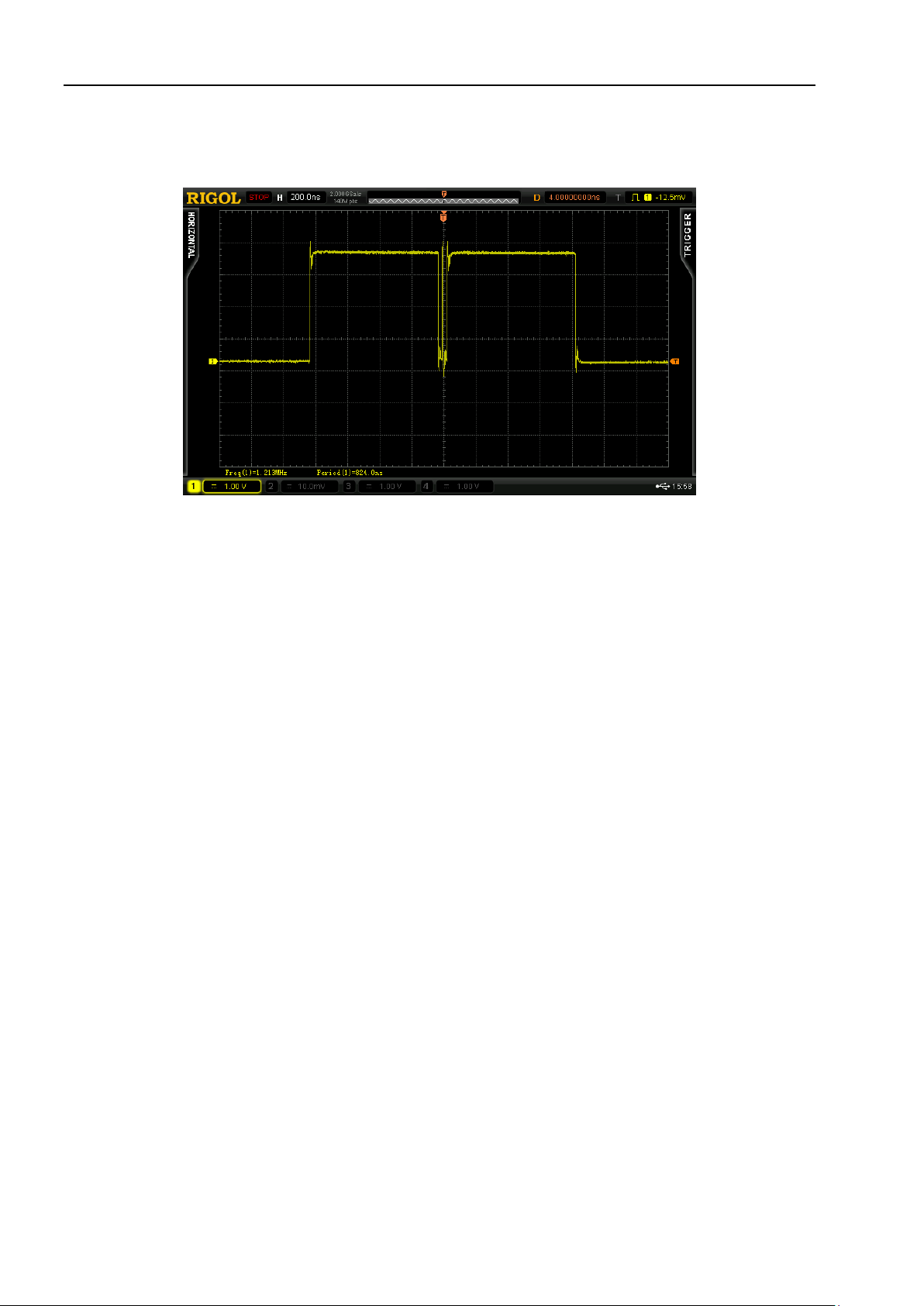
Set the time base to 5ms. At this point, the sample rate is 2GSa/s and the memory depth is
140Mpts. Under single trigger, every burst can be captured as shown in the figure below.
Figure 3-29 Manual Burst Signal
Find Quality Products Online at: [email protected]
User’s Guide for DS6000 Demo Board 3-25
www.GlobalTestSupply.com
Page 36
RIGOL Chapter 3 Demo Board Applications
3-26
Adjust the time base to 200ns/div when the oscilloscope is in STOP state and amplify the
waveform captured. As shown in the figure below, all the waveform details are successfully
captured. As DS6000 provides a 140Mpts deep memory, users can adjust the horizontal position
to view relatively longer waveform stored.
Figure 3-30 Burst Details
Find Quality Products Online at: [email protected]
www.GlobalTestSupply.com
User’s Guide for DS6000 Demo Board
Page 37
Chapter 3 Demo Board Applications RIGOL
3.2.9 Narrow Burst Signal
1. Signal Explanation
Signal Output Pin: PULSE_OUT
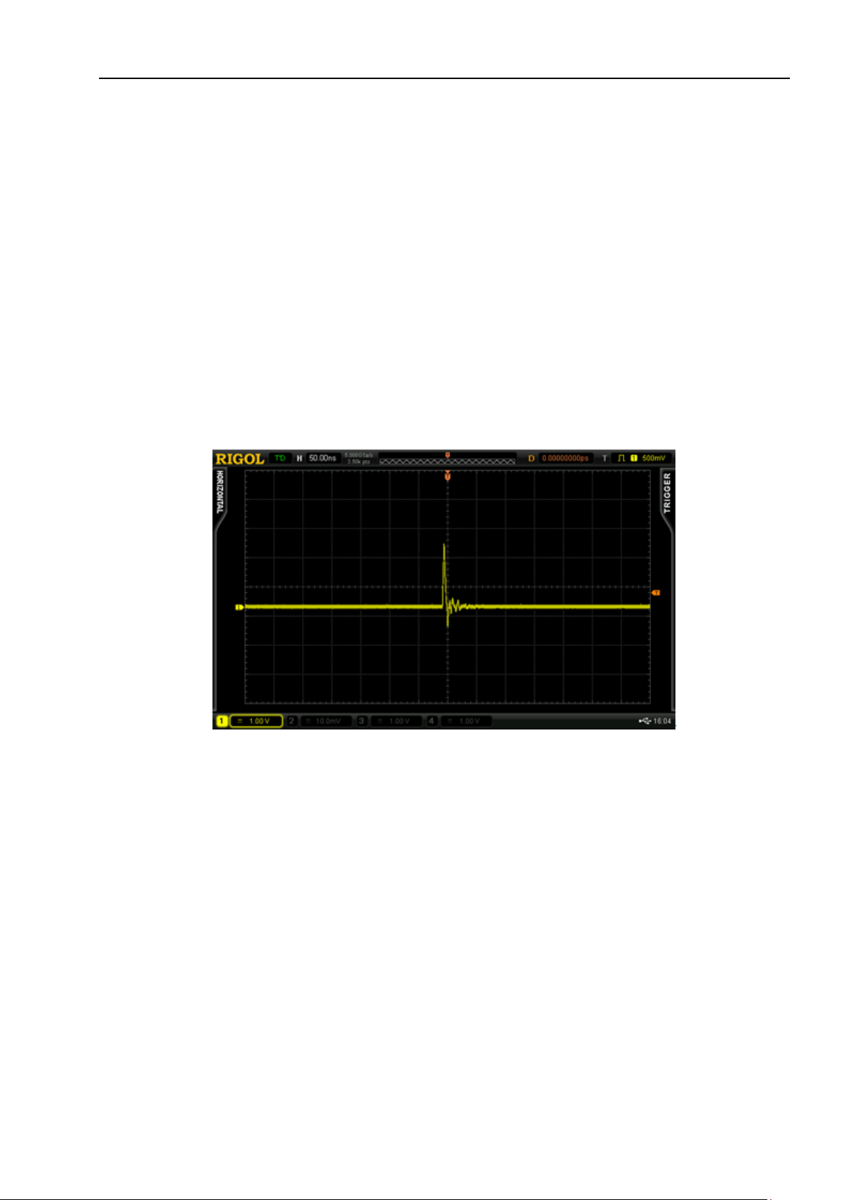
Narrow pulse signal with 100us period and 2ns width.
2. Functions
Pulse trigger
3. Demonstration and Result
Connect the signal output pin PULSE_OUT and GND to CH1 of the oscilloscope properly using
the probe.
Set the trigger type to “Pulse”, the trigger condition to <4ns, the trigger mode to “Auto” and the
vertical scale to “1 V”; adjust the vertical position and trigger level to appropriate values. The
demonstration result is as shown in the figure below.
Figure 3-31 Narrow Pulse
Find Quality Products Online at: [email protected]
User’s Guide for DS6000 Demo Board 3-27
www.GlobalTestSupply.com
Page 38
RIGOL Chapter 3 Demo Board Applications
3-28
3.2.10 Glitch Signal of Sine
1. Signal Explanation
Signal Output Pin: GLITCH_SINE
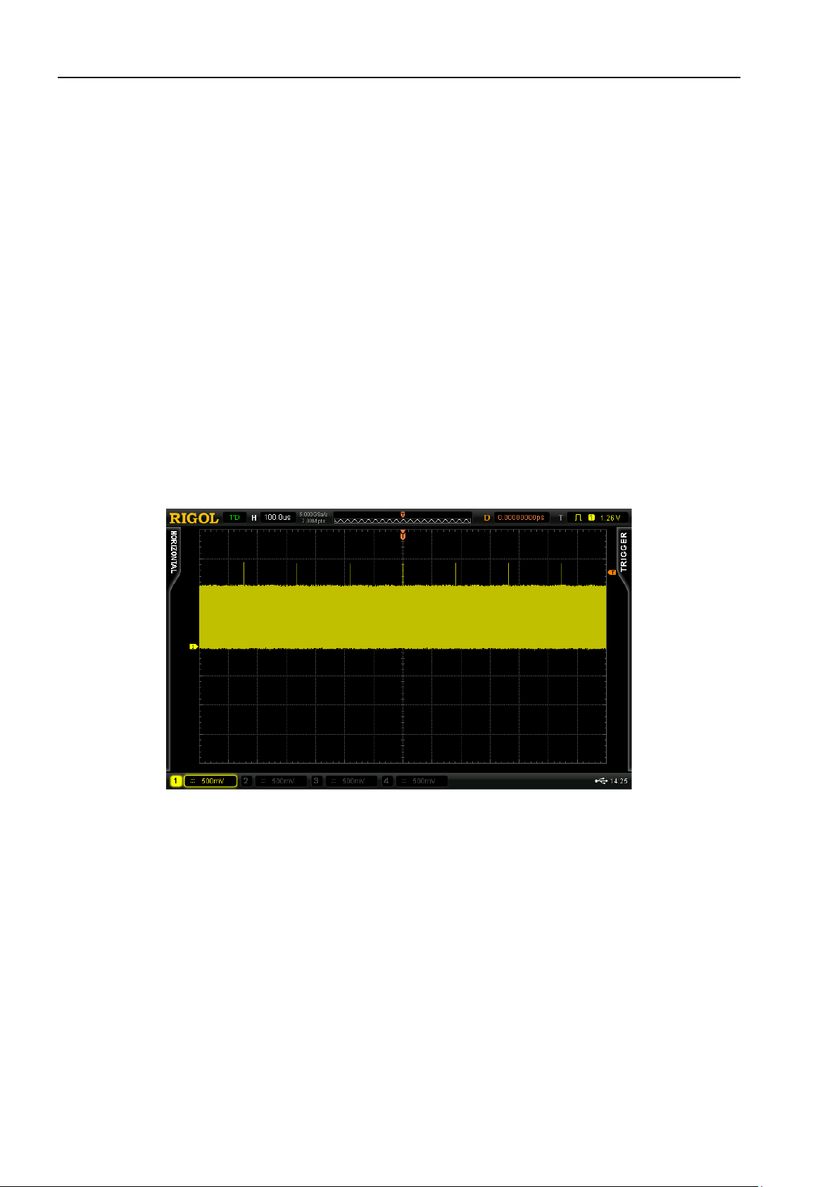
The sine frequency is 500kHz, the glitch width is 2ns, the glitch occurrence period is about 90us
and the position of the glitch is not fixed.
2. Functions
Pulse trigger, multi-level gray scale
3. Demonstration and Result
Connect the signal output pin GLITCH_SINE and GND to CH1 of the oscilloscope properly using
the probe;
Set the trigger type to “Pulse”, the trigger condition to <10ns and the trigger mode to “Auto”;
adjust the time base to 100us and set the acquisition mode to “Normal” and the vertical scale to
“500 mV”; adjust the vertical position and trigger level to appropriate values to make the
oscilloscope trigger stably. The demonstration result is as shown in the figure below and users
can view the interval time between glitches. All the adjacent glitches can be captured.
Figure 3-32 Sine Glitch Signal
Find Quality Products Online at: [email protected]
www.GlobalTestSupply.com
User’s Guide for DS6000 Demo Board
Page 39
Chapter 3 Demo Board Applications RIGOL
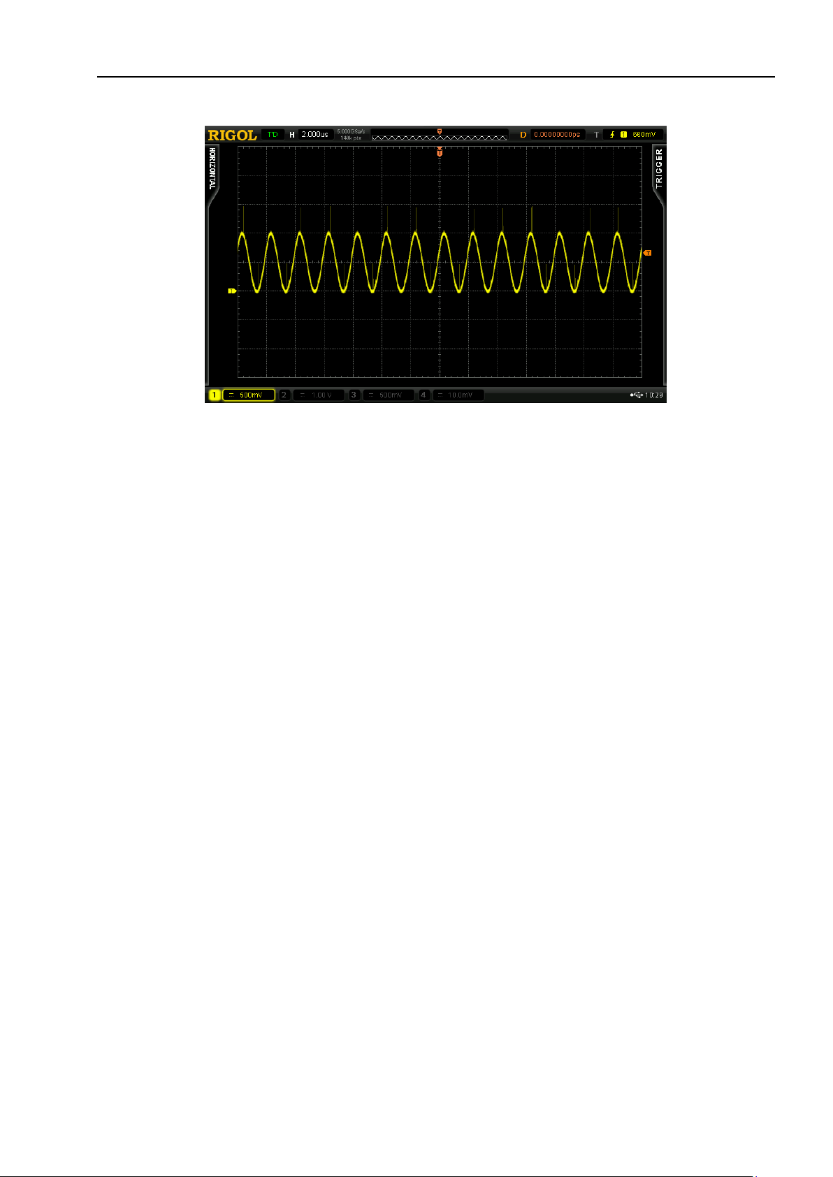
Set the time base to 2us. The demonstration result is as shown in the figure below and the
positions of the glitches on the sine waveform are clearly displayed.
Figure 3-33 Sine Glitch Signal (Details)
Find Quality Products Online at: [email protected]
User’s Guide for DS6000 Demo Board 3-29
www.GlobalTestSupply.com
Page 40
RIGOL Chapter 3 Demo Board Applications
3-30
3.2.11 Glitch Signal of Square Waveform
1. Signal Explanation
Signal Output Pin: GLITCH_CLK
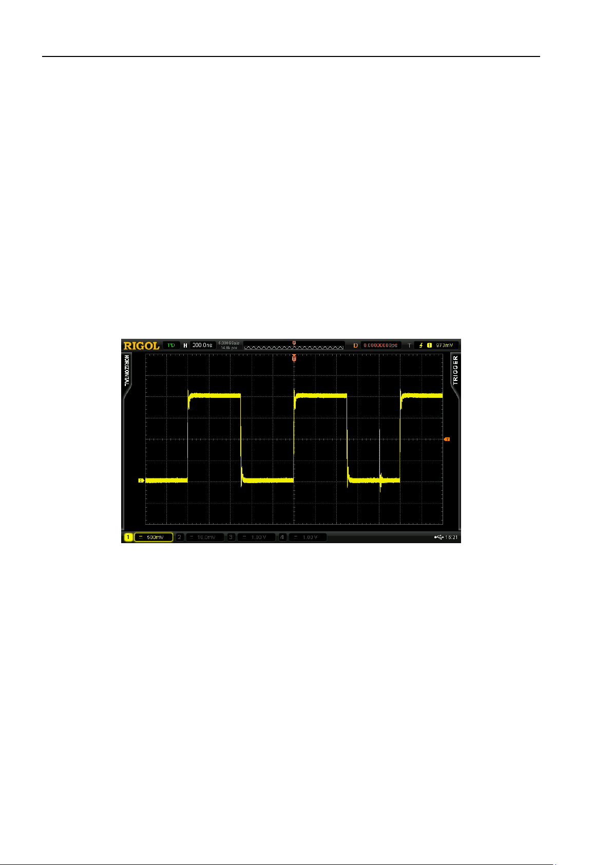
The frequency of the square waveform is 1MHz, the glitch width is 2ns and the position of the
glitch is not fixed.
2. Functions
Edge trigger, pulse trigger
3. Demonstration and Result
Connect the signal output pin GLITCH_CLK and GND to CH1 of the oscilloscope properly using
the probe;
Set the trigger type to “Edge”, the signal source to “CH1”, the edge type to “Leading”, the trigger
mode to “Normal” and the vertical scale to “500 mV”; adjust the vertical position and trigger
level to appropriate values. The demonstration result is as shown in the figure below.
Figure 3-34 Square Waveform Glitch Signal
Find Quality Products Online at: [email protected]
www.GlobalTestSupply.com
User’s Guide for DS6000 Demo Board
Page 41
Chapter 3 Demo Board Applications RIGOL
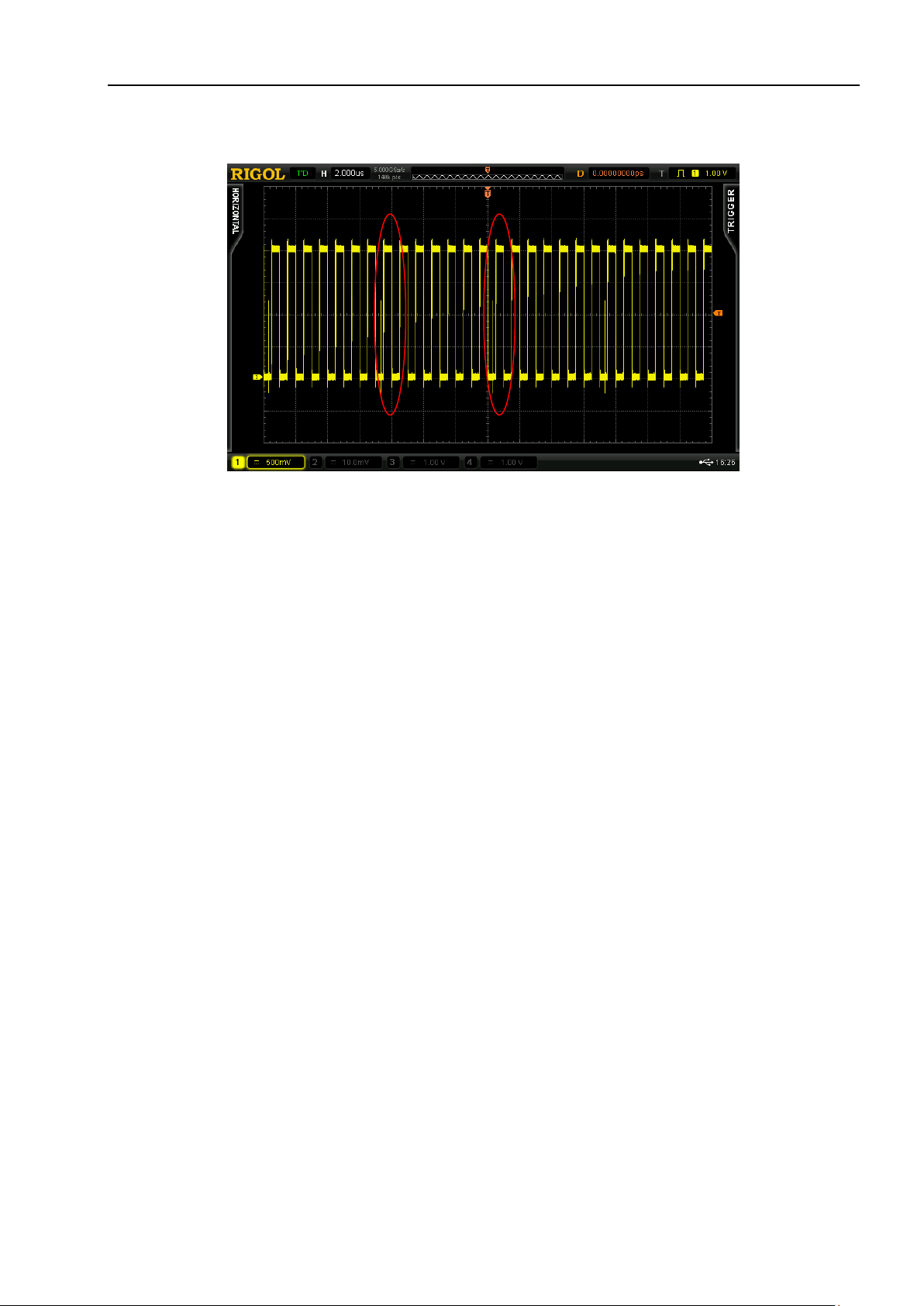
Set the trigger type to “Pulse”, the pulse condition to <10ns, the trigger mode to “Normal” and
the time base to 2us; the demonstration result is as shown in the figure below and users can
view the interval time between glitches.
Figure 3-35 Time Interval between Glitches
Find Quality Products Online at: [email protected]
User’s Guide for DS6000 Demo Board 3-31
www.GlobalTestSupply.com
Page 42
RIGOL Chapter 3 Demo Board Applications
3-32
3.2.12 Crosstalk Signal
1. Signal Explanation
Signal Output Pin: CTALK_A, CTALK_B
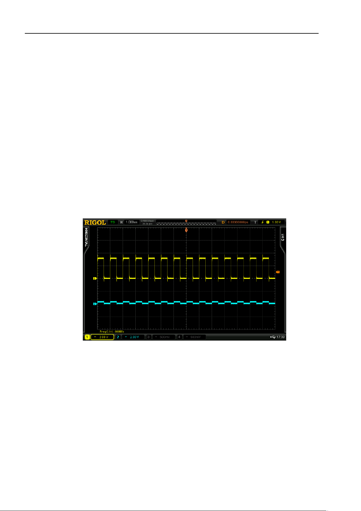
The two pins output 1 MHz low-frequency square waveforms. Press SINGLE to trigger the 125
MHz high-frequency signal.
2. Functions
Bandwidth limit, crosstalk demonstration
3. Demonstration and Result
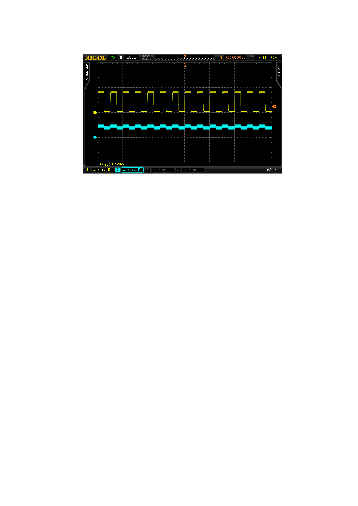
Connect CTALK_B and GND to CH1 of the oscilloscope using the probe;
Connect CTALK_A and GND to CH2 of the oscilloscope using the probe;
Set the vertical scale of CH1 and CH2 to “2 V”, the trigger type to “Edge”, the signal source to
“CH1”, the edge type to “Leading” and the trigger mode to “Auto”; adjust the trigger level to an
appropriate value to make the oscilloscope trigger stably. The demonstration result is as shown
in the figure below. As the frequency measurement result in the figure shows, the frequency of
the signal is 1 MHz.
Figure 3-36 CTALK_A and CTALK_B Output Signals
Find Quality Products Online at: [email protected]
www.GlobalTestSupply.com
User’s Guide for DS6000 Demo Board
Page 43
Chapter 3 Demo Board Applications RIGOL
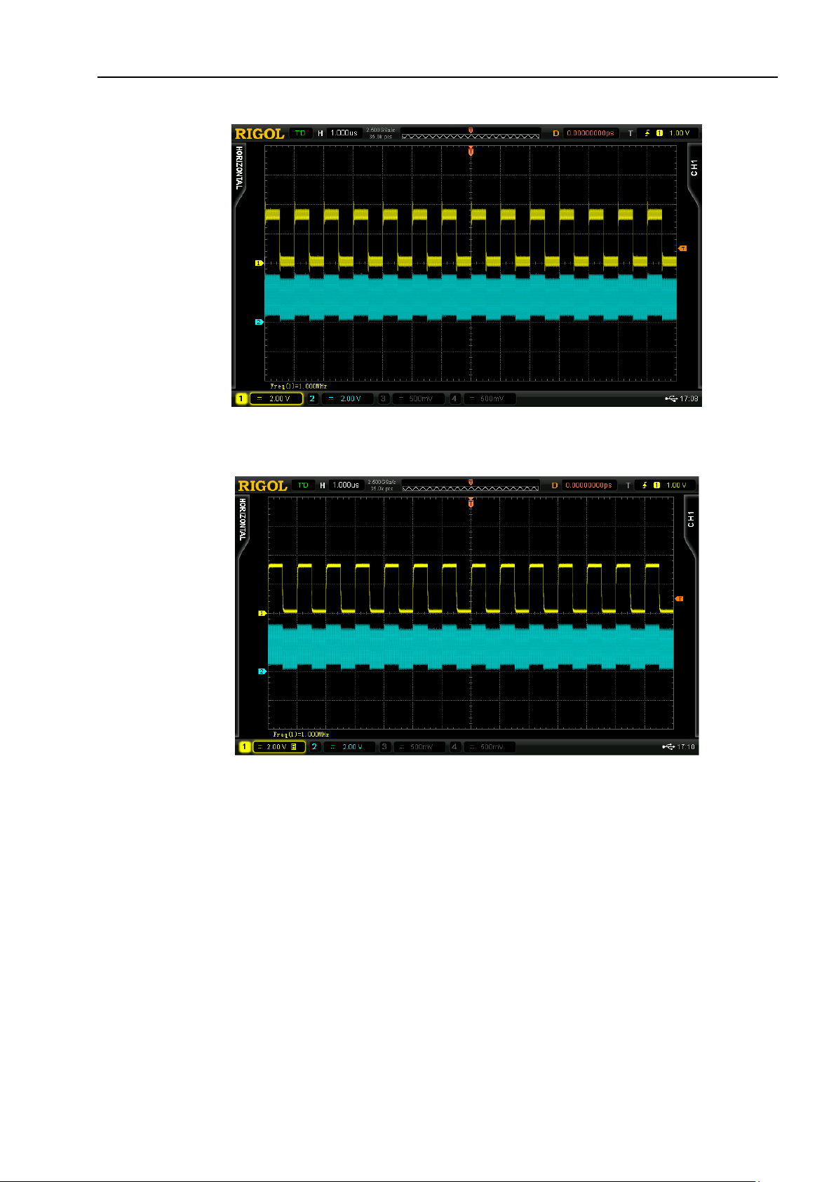
Press SINGLE to trigger the 125 MHz high-frequency signal. The demonstration result is as
shown in the figure below.
Figure 3-37 Crosstalk Signal Demonstration Result
Enable the 20MHz bandwidth limit of CH1 and press SINGLE to trigger the 125 MHz
high-frequency signal. The demonstration result is as shown in the figure below.
Figure 3-38 Enable 20MHz Bandwidth of CH1
Find Quality Products Online at: [email protected]
User’s Guide for DS6000 Demo Board 3-33
www.GlobalTestSupply.com
Page 44
RIGOL Chapter 3 Demo Board Applications
3-34
Enable the 20MHz bandwidth limit of CH2 and press SINGLE to trigger the 125 MHz
high-frequency signal. The demonstration result is as shown in the figure below.
Figure 3-39 Enable 20MHz Bandwidth Limit of CH2
Find Quality Products Online at: [email protected]
www.GlobalTestSupply.com
User’s Guide for DS6000 Demo Board
Page 45
Chapter 3 Demo Board Applications RIGOL
3.3 Digital Signal Applications
3.3.1 RS232/UART Signal
1. RS232 Protocol Explanation
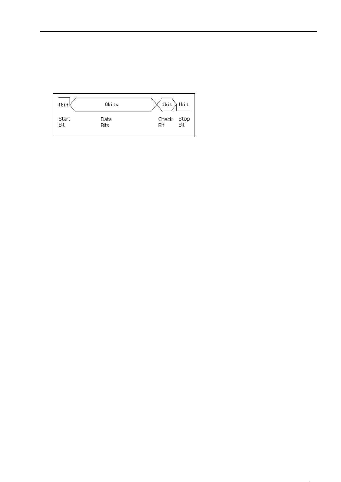
The start bit is always high level; the data bits is always 6bits, 7bits or 8bits. It is fixed at 8bits in
this Demo board;
By default, the data polarity is negative (namely high level stands for logic 0 and low level stands
for logic 1);
Check bit usually contains odd check, even check and none. For this Demo board, RS232 signal
does not have check bit;
Stop bit is always 1bit, 1.5bits or 2bits. For this Demo board, the stop bit of RS232 signal is 1bit.
2. Signal Explanation
Signal Output Pin: RS232_TX
Rate: 9600bps; Data: RIGOL DS6000; Frame structure: 1bit start bit+ 8bits data bits+ 1bit stop
bit; LSB output; negative polarity, none (check bit)
3. Functions
RS232 trigger, RS232 decoding
4. Demonstration and Result
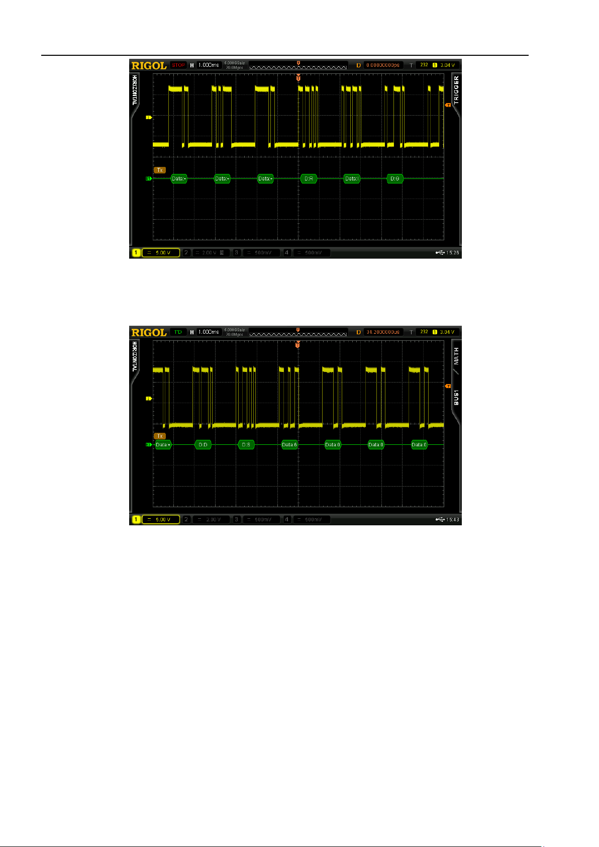
Connect the signal output pin RS232_TX and GND to CH1 of the oscilloscope properly using the
probe;
Set the trigger type to “RS232”, the signal source to “CH1”, the trigger condition to “Start”, the
baud rate to “9600bps” and the trigger mode to “Auto”; adjust the vertical position and trigger
level to appropriate values to make the oscilloscope trigger stably;
When the oscilloscope is in T’D mode, set the decoding type to “RS232”, TX to “CH1”, RX to
“OFF”, the polarity to “-”(negative), the data bits to “8”, the stop bit to “1 bit”, the even-odd
check bit to “None”, the ary to “ASCII” and TX threshold to 1.36V. Set the BUS status to “ON”
and the demonstration result is as shown in the figure on the next page.
Find Quality Products Online at: [email protected]
User’s Guide for DS6000 Demo Board 3-35
www.GlobalTestSupply.com
Page 46
RIGOL Chapter 3 Demo Board Applications
3-36
Figure 3-40 RS232 Trigger and Decoding
Set the trigger condition to “Data” and the data to “54” (the ASCII code value of “6”). The
corresponding data can be captured stably.
Figure 3-41 RS232 Trigger and Decoding (Data Trigger)
Find Quality Products Online at: [email protected]
www.GlobalTestSupply.com
User’s Guide for DS6000 Demo Board
Page 47
Chapter 3 Demo Board Applications RIGOL
Error Identifier
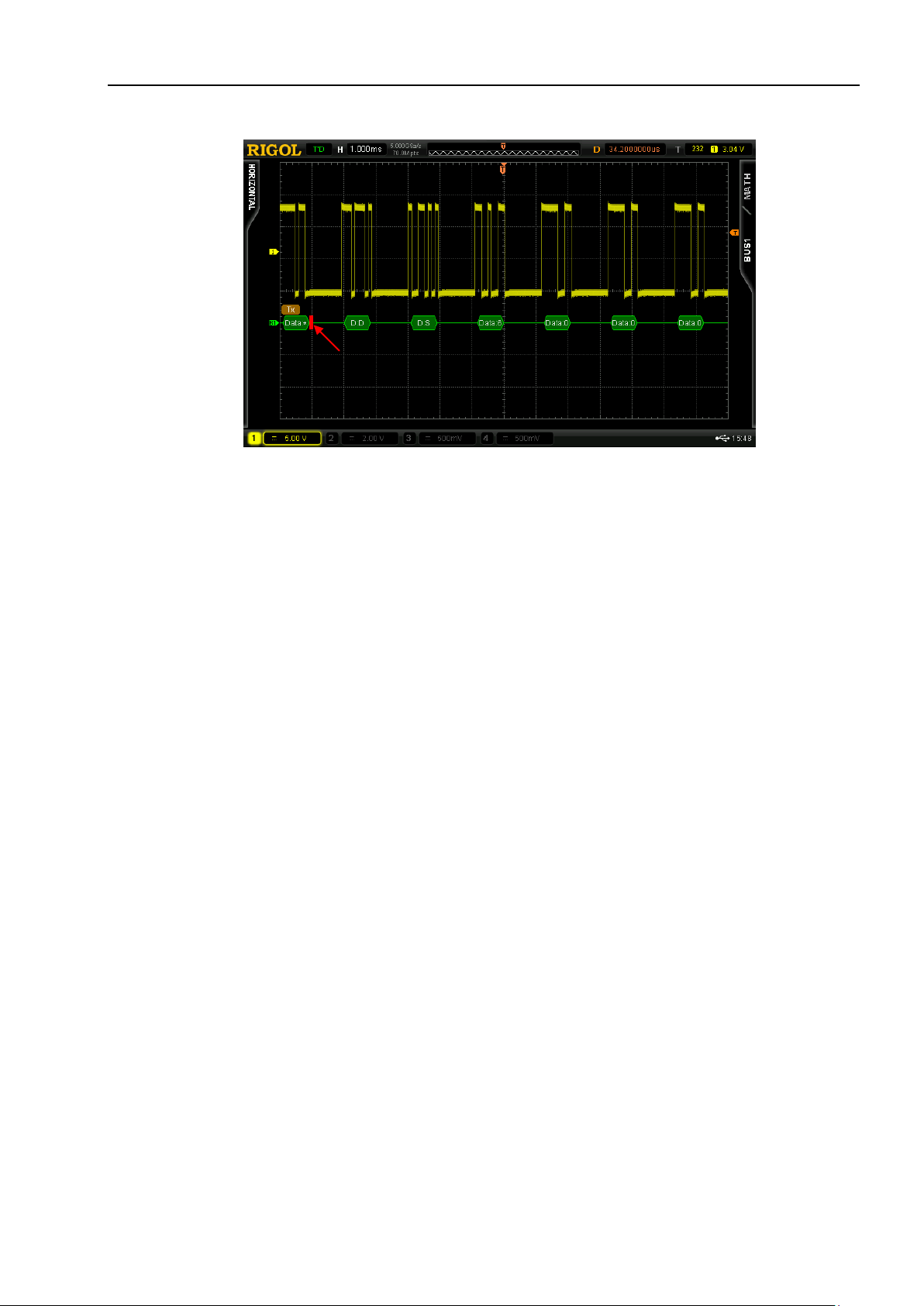
Set the check mode to “Odd” in the decoding menu during the above-mentioned data trigger. As
data on the Demo board does not contain check bit, red error identifier is displayed.
Figure 3-42 RS232 Trigger and Decoding (Odd Check)
Note: the output signal of pin UART is the same with the RS232_TX signal except that its polarity is
positive. The same demonstration result can be obtained using the above method (set the polarity to “+”
in protocol decoding).
Find Quality Products Online at: [email protected]
User’s Guide for DS6000 Demo Board 3-37
www.GlobalTestSupply.com
Page 48
RIGOL Chapter 3 Demo Board Applications
3-38
3.3.2 SPI Signal
1. Protocol Explanation
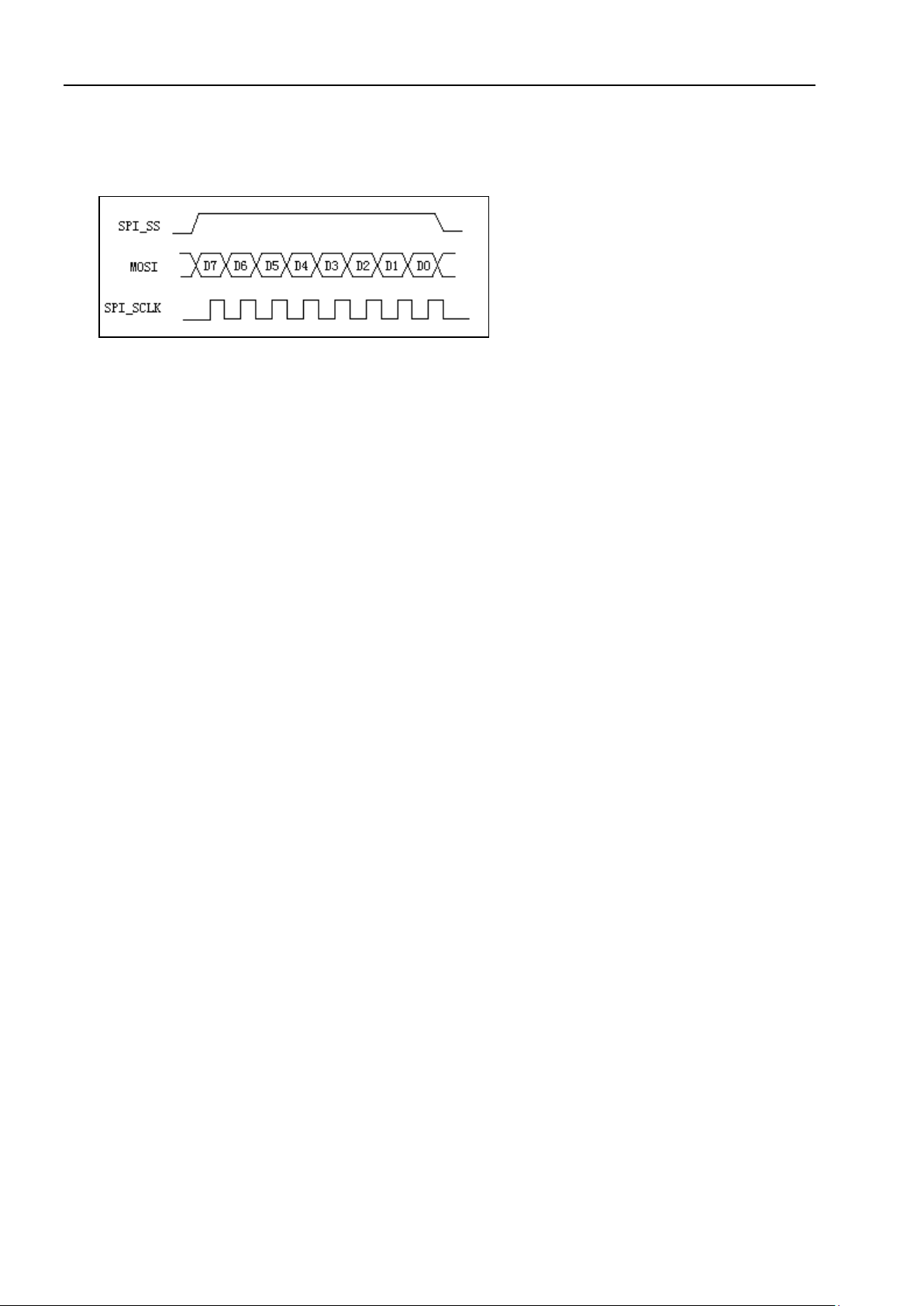
Clock signal and data appears synchronously. Sample the data on the rising edge of the clock
signal.
The continuous clock or data is one frame.
SS: select positive or negative polarity. When positive polarity is selected, the oscilloscope starts
decoding when the SS pin is logic low.. When negative polarity is selected, the oscilloscope
starts decoding when the SS pin is logic high.
For the data bus, every 8bit is a byte and every frame can contain 1 byte, 2 bytes or 3 bytes. In
the figure above, the frame contains 1 byte.
2. Signal Explanation
Signal Output Pin: SPI_SS, SPI_MOSI, SPI_SCLK
The output Data increases steadily from 0 to 255 and the bits of every frame of data can be
8/16/24/32
3. Functions
SPI trigger, SPI decoding
4. Demonstration and Result
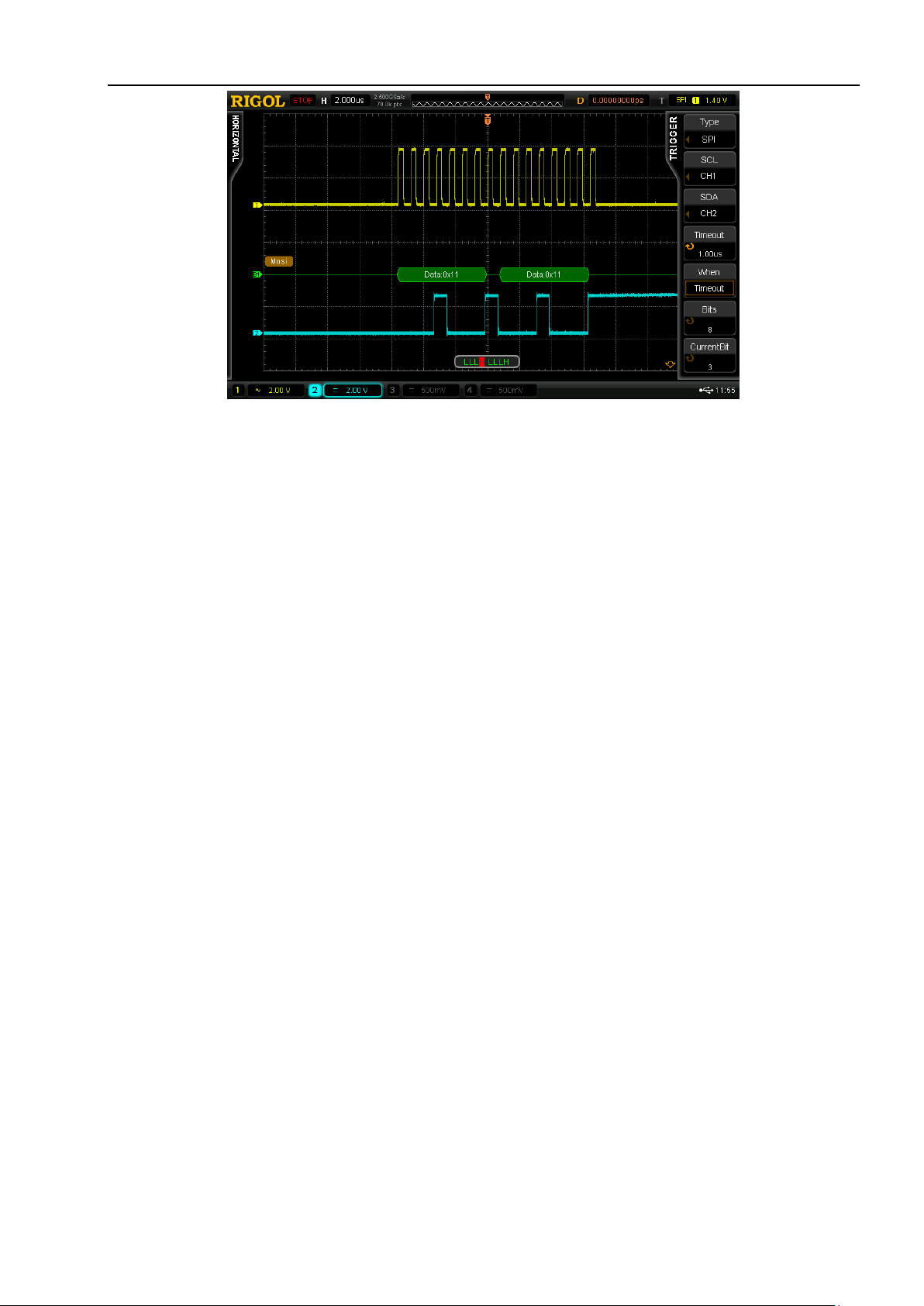
Connect SPI_SCLK and GND to CH1 using the probe; connect SPI_MOSI and GND to CH2 using
the probe;
Set the trigger type to “SPI”, SCL to “CH1”, SDA to “CH2”, the trigger condition to “Timeout”, the
bits to 8, the data to “LLLH LLLH” and the clock edge to “Leading”.
When the oscilloscope is in T’D mode, set the decoding type to “SPI”, SS and MISO to “OFF”,
SCLK to “CH1”, MOSI to “CH2”, the data bits to 8, the endian to MSB and the ary to hex. Set the
BUS status to “ON” and the demonstration result is as shown in the figure on the next page.
Find Quality Products Online at: [email protected]
www.GlobalTestSupply.com
User’s Guide for DS6000 Demo Board
Page 49
Chapter 3 Demo Board Applications RIGOL
Figure 3-43 SPI Trigger and Decoding
Find Quality Products Online at: [email protected]
User’s Guide for DS6000 Demo Board 3-39
www.GlobalTestSupply.com
Page 50
RIGOL Chapter 3 Demo Board Applications
3-40
3.3.3 I2C Signal
1. Protocol Explanation
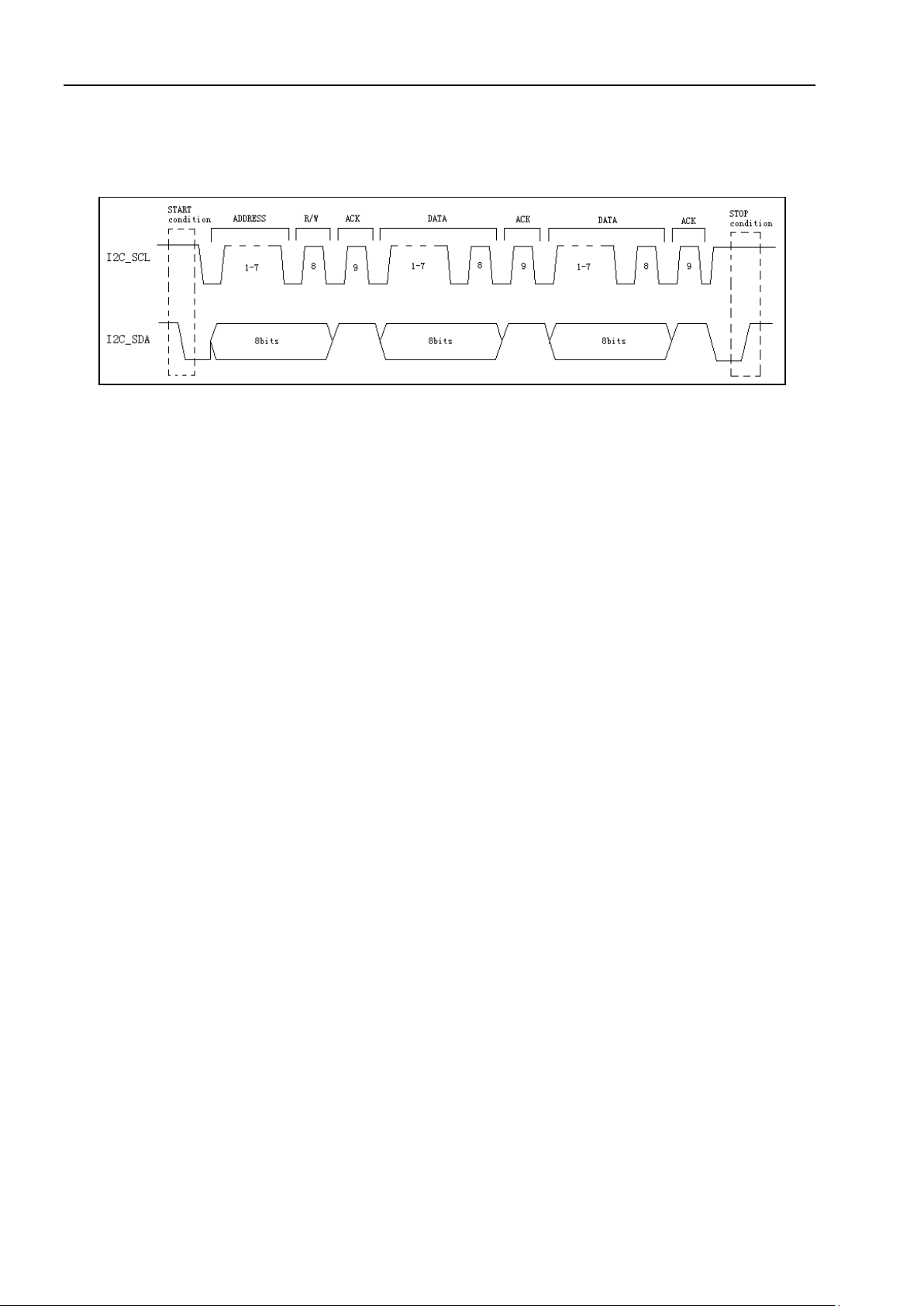
The start condition: when SCL is high level and SDA switches from high level to low level.
The stop condition: when SCL is high level and SDA switches from low level to high level.
The 8bits following the start condition is the slave device address and the read/write bit. The
address bit can also be 10bits and at this point, it occupies two bytes.
When the read/write bit is 0, the oscilloscope sends data (write); and when it is 1, the
oscilloscope reads data (read).
Every time a byte is sent by the host device, the slave device is asked to send a answer signal
and at this point, the host device restores to the high level; if the signal is successfully received
by the slave device, the level of the answer bit drops and if the signal is not successfully received,
the answer bit holds in high level.
2. Signal Explanation
Signal Output Pin: I2C_SCL, I2C_SDA
I2C signal with 125 kHz rate. The content is “RIGOL”. The data frame head and the read/write
bit would change.
3. Functions
I2C trigger, I2C decoding
4. Demonstration and Result
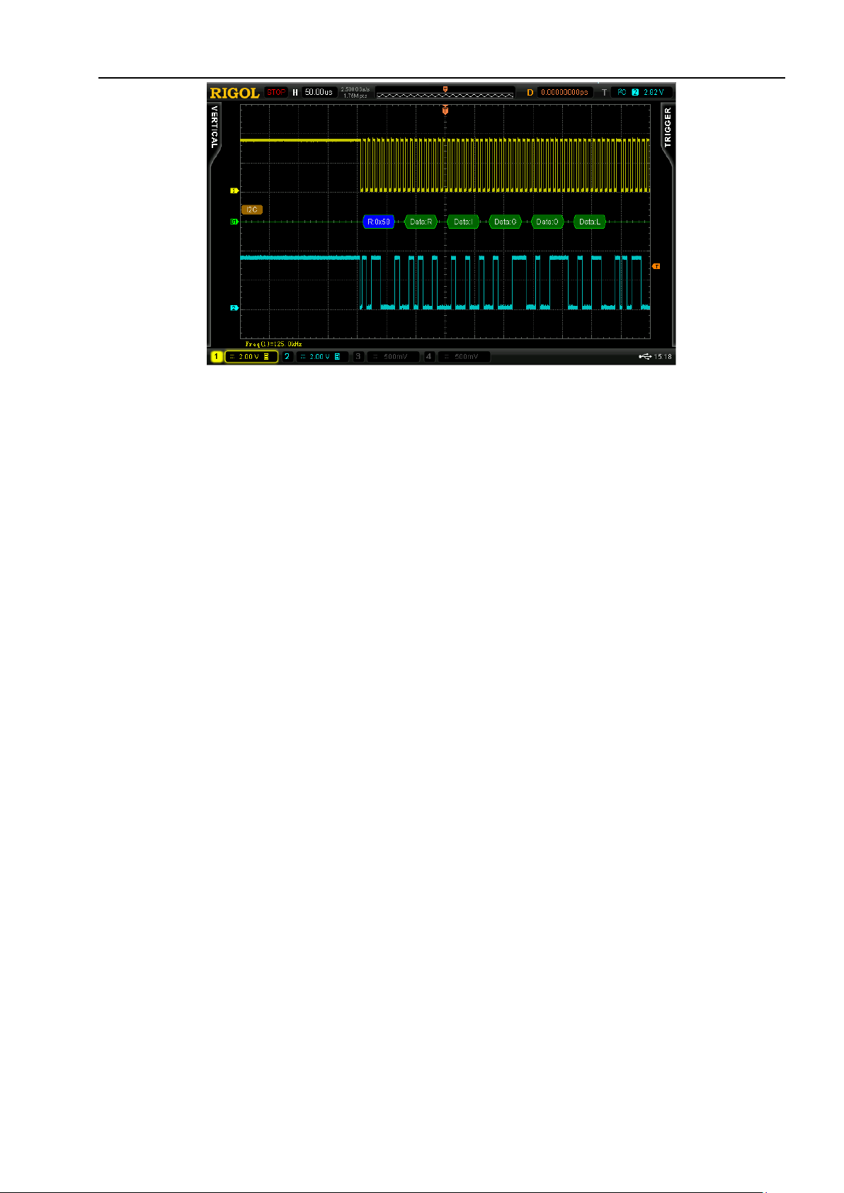
Connect I2C_SCL and GND to CH1 properly using the probe; connect I2C_SDA and GND to CH2
properly using the probe.
Set the trigger type to “I2C”, SCL to “CH1”, SDA to “CH2”, the trigger condition to “Data”, the
data to “LHLH LLHL” (namely the decimal number 82 and the ASCII code of the character “R”)
and the trigger mode to “Auto”; adjust the vertical position and trigger level to appropriate
values to make the oscilloscope trigger stably.
When the oscilloscope is in T’D state, set the decoding type to “I2C”, the ary to “ASCII”, the SCLK
threshold to “1.00V” and the SDA threshold to “1.00V”. Set the BUS status to “ON” and the
demonstration result is as shown in the figure on the next page.
Find Quality Products Online at: [email protected]
www.GlobalTestSupply.com
User’s Guide for DS6000 Demo Board
Page 51
Chapter 3 Demo Board Applications RIGOL
Figure 3-44 I2C Trigger and Decoding
Find Quality Products Online at: [email protected]
User’s Guide for DS6000 Demo Board 3-41
www.GlobalTestSupply.com
Page 52
RIGOL Chapter 3 Demo Board Applications
3-42
SOF
Identifier
DLC
Data
CRC
ACK
EOF
3.3.4 CAN Signal
1. Protocol Explanation
1) The frame types include data frame, remote frame, error frame, overload frame and frame
interval.
2) Standard format of data frame:
SOF: represents frame start;
Identifier: represents the ID of the data frame and is used to determine the priority of the
frame;
DLC: represents the length of the data;
Data: data segment. It can contain 0 to 8 bytes of data and is output from MSB (the highest bit);
CRC: CRC check segment;
ACK: used to determine whether the data is successfully received or not.
2. Signal Explanation
Signal Output Pin: CAN_L, CAN_H
CAN signal with 1MHz signal rate. The data is the character string “RIGOL”; the data length is 5;
the signal uses CRC check and does not have ACK segment.
3. Functions
CAN trigger, CAN decoding
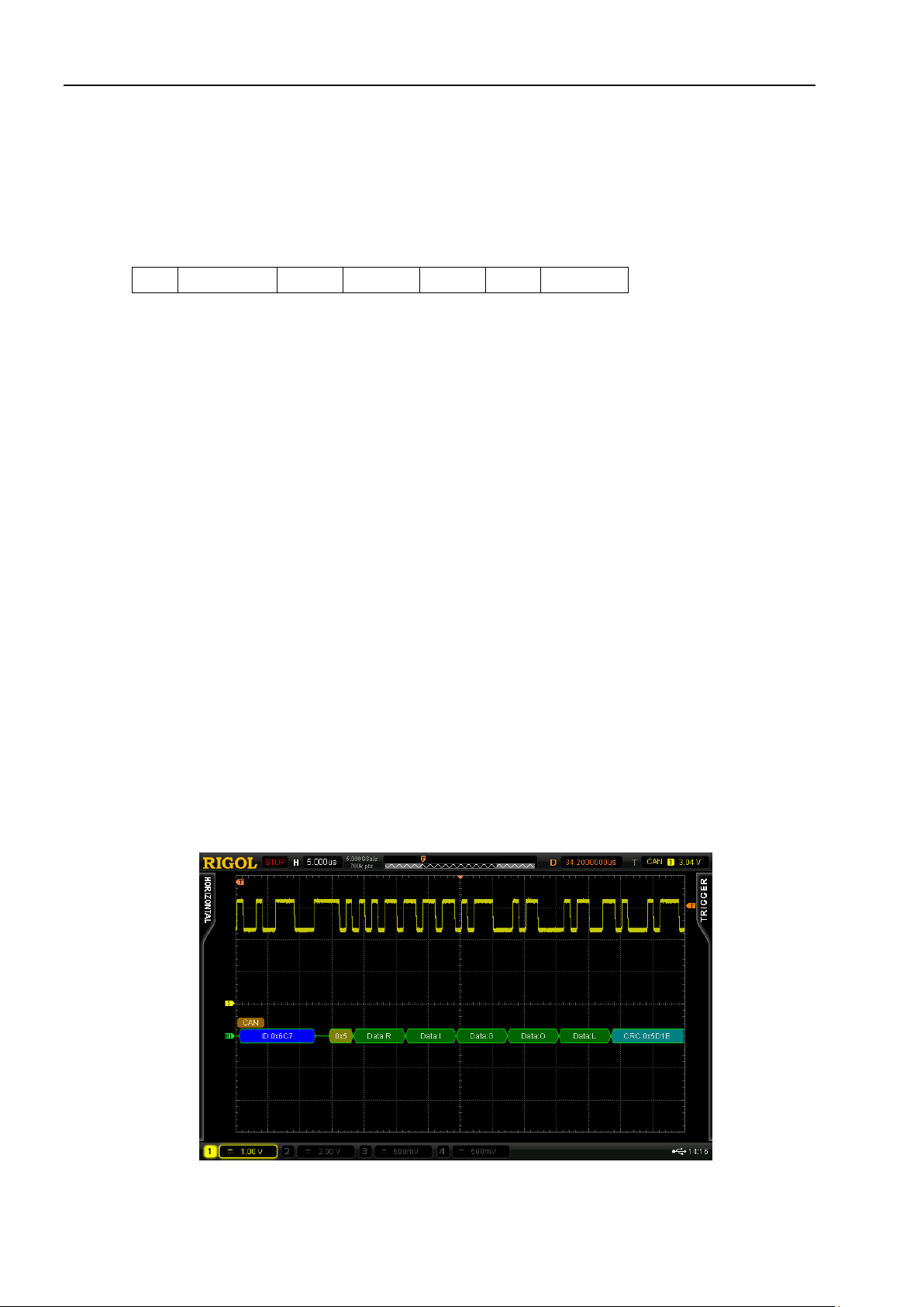
4. Demonstration and Result
Connect the signal output pin CAN_H and GND to CH1 of the oscilloscope properly using the
probe;
Set the trigger type to “CAN”, the signal source to “CH1”, the signal type to “CAN_H”, the trigger
condition to “SOF”, the baud rate to “1Mb/s” and the trigger mode to “Auto”.
When the oscilloscope is in T’D state, set the decoding type to “CAN” and the ary to ASCII. Set
the BUS status to “ON” and the demonstration result is as shown in the figure below.
Figure 3-45 CAN Trigger and Decoding
Find Quality Products Online at: [email protected]
www.GlobalTestSupply.com
User’s Guide for DS6000 Demo Board
Page 53
Chapter 3 Demo Board Applications RIGOL
3.3.5 Signals for Testing Logic Analyzer
1. Signal Explanation
Signal Output Pin: LA_D0~LA_D15
16-channel parallel data (from D0 to D15). Wherein, the frequency of D0 is a half of 25MHz, the
frequency of D1 is a half of the frequency of D0 and so on.
2. Functions
Logic analyzer
3. Demonstration and Result
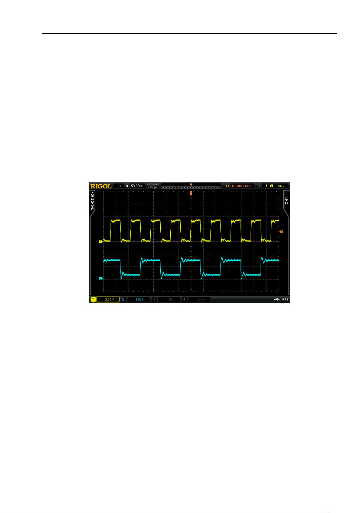
Connect LA_D0 and GND to CH1 of the oscilloscope using the probe; connect LA_D1 and GND to
CH2 of the oscilloscope using the probe. The demonstration result is as shown in the figure
below.
Figure 3-46 LA_D0 and LA_D1 Output Signals
Find Quality Products Online at: [email protected]
User’s Guide for DS6000 Demo Board 3-43
www.GlobalTestSupply.com
Page 54
RIGOL Chapter 3 Demo Board Applications
3-44
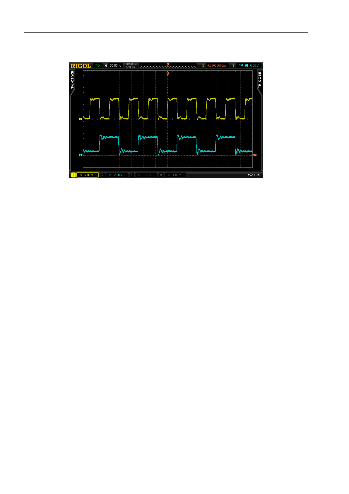
Set the trigger mode to “Pattern” (pattern trigger uses the logic relation between the two
channels as trigger condition) and the trigger positions of CH1 and CH2 to “Leading” and “X”,
respectively. The oscilloscope can trigger stably as shown in the figure below.
Figure 3-47 LA_D0 and LA_D1 Output Signals (Pattern Trigger)
Find Quality Products Online at: [email protected]
www.GlobalTestSupply.com
User’s Guide for DS6000 Demo Board
 Loading...