

Page 1

SECTION 1
OVERALL MACHINE
INFORMATION
Page 2

Overall
Information
1 February 1994 SPECIFICATIONS
1. SPECIFICATIONS
Copy Process: Laser electrostatic transfer system
Originals: Book/sheet, fixed platen
Original Alignment: Front-right corner
Maximum Original Size: 11" x 17"/A3
Copy Paper Size: Maximum: 11" x 17"/A3
Minimum: 5
1/2" x 81/2"/A5
Copy Paper Weight: Bypass feed: 17 to 42 lb/64 to 157 g/m
Side cassette: 17 to 42 lb/64 to 157 g/m
Front trays: 17 to 28 lb/64 to 104 g/m
Copying Speed: 30 copies per minute (81/2" x 11" sideways)
31 copies per minute (A4 sideways)
18 copies per minute (11" x 17")
18 copies per minute (A3)
First Copy: 5.8 seconds (8
1/2" x 11"/A4 sideways) from
side cassette
Warm-up Time: Within 5 minutes
(Room temperature 23°C/73°F)
Copy Counters:
Set counter: 1 to 999 (max. is adjustable by SP mode)
Copy counter: 1 to 999 ( count-up or count-down, can be
selected by SP mode)
Paper Capacity: Cassette: 250 sheets
Manual feed table: 30 sheets
2
2
2
Copy Tray Capacity: 250 sheets (8
1/2" x 14"/B4 and smaller)
100 sheets (11" x 17"/A3)
Automatic Reset: After 60 seconds (3 min. can be selected by
SP mode)
-- Reproduction Ratio: Full size
-- Interrupt Mode: OFF
-- 2 Single Copies: OFF
-- Sort/Stack: OFF
* : It is possible to be changed by
SP mode
-- Duplex: OFF
-- Set Counter: 1
-- Copy Counter: 0
1-1
Page 3

SPECIFICATIONS 1 February 1994
-- Image Density: Auto ID *
-- User Program Mode: OFF
-- Total Area Editing: OFF
-- Letter/Photo mode: Letter mode
-- Designated Area Editing: OFF
-- Cassette: 1st or LCT *
-- Auto Reduce/Enlarge: OFF
-- Auto Paper Selection: ON *
Photoconductor: Organic photoconductor drum
Drum Charge: Dual-wire with grid plate (Negative Charge)
Fixed Reproduction Ratios: 6 enlargement ratios and 7 reduction ratios
A4/A3 version LT/LDG version
800%
400%
Enlargement
Full Size 100% 100%
Reduction
200%
141%
122%
115%
93%
82%
75%
71%
65%
50%
25%
800%
400%
200%
155%
129%
121%
93%
85%
77%
74%
65%
50%
25%
Zoom: From 25% to 800% in 1% increments.
Allows independent horizontal and vertical
percentage.
Scanning System: CCD, one directional scanning with mirrors
and lens
Picture Element Density: 400 dots per inch (15.7 lines/mm)
Scanner Light Source: Two fluorescent lamps (green light)
Exposure System: Semiconductor laser, one dimensional
scanning
Development:
• Dual-component dry toner system
• Double roller development
Toner Replenishment: 300 gram cartridge
1-2
Page 4

Overall
Information
1 February 1994 SPECIFICATIONS
Toner Consumption: 5,500 copies/cartridge
1/2" x 11"/A4, 6% Originals)
(8
Development Bias: Negative fixed bias
Toner Density Control: Pattern density detection by photosensor
Image Transfer: Single wire dc (positive charge)
Paper Separation: Dual wire ac corona and pick-off pawls
Cleaning: Cleaning blade, cleaning brush, and
pre-cleaning corona
Quenching: Photo quenching by LEDs
Paper Feed System: Feed and reverse roller
Image Fusing: Heat and pressure type, teflon (upper) and
silicone rubber (lower) rollers
Fusing Lamp: Halogen lamp (115 V, 750 W/230 V, 800 W)
Silicone Oil Consumption: More than 80,000 copies/500 cc
1/2" x 11"/A4 copies)
(8
Printer Feature
Memory: Instruction ROM: 4 Mbytes
Font ROM: 2 Mbytes
Base RAM: 8 Mbytes
PDL/Emulation: Adobe PostScript Level 2
HP LaserJet
compatible with HP LaserJet
ΙΙΙ (PCL-5) Emulation and
ΙΙΙsi, ΙΙD
Graphics:
Compressed files: Decompress raster graphic files (as per
Adobe PS 2 and HP PCL 5 specifications)
Conversion: Automatically convert 300 dpi bit-mapped
graphics for HP PCL 5 mode.
1-3
Page 5

SPECIFICATIONS 1 February 1994
Fonts:
Adobe type 1: Outline fonts: Zapf Chancery, Zapf Dingbats,
Symbol plus four styles (normal, italic, bold,
bold-italic) each of Avant Garde Bookman,
Courier, Helvetica, Helvetica Narrow, New
Century Schoolbook, Times Palatino
HP/Intellifonts: Outline fonts: Zapf Dingbats plus four styles
(normal, italic, bold, bold-italic) each of
Univers, Univers Condensed, CG Times
Soft font capability: Outline fonts downloadable to memory or
optional hard disk
Printer Port: RS232C serial
Bi-directional Centronics parallel
RS422 Appletalk
Scanner Feature
Scan Area: Max. 11" x 17"/A3
Scan Time: Max. 2 seconds (8
1/2" x 11"/A4 at full size
mode (400 dpi)
Document Type: Book/Sheet
Image Reduction: 25% (100 dpi) 50% (200 dpi) 75% (300 dpi)
Output Data: Binary Digital Data
-- Black and White (fixed threshold)
-- Photo Mode (dither pattern)
Brightness: From 1 to 7
Host Interface: SCSI-II
Self-diagnostic Codes: 35 codes, indicated in the guidance display
Power Source:
115 V/60 Hz/15 A, 220
∼ 240 V/50 Hz/8 A
Power Consumption: Maximum: 1.50 kW
Warm-up: 0.9 kW (average)
Copy cycle: 1.1 kW (average)
Stand-by: 0.15 kW
1-4
Page 6

Overall
Information
1 February 1994 SPECIFICATIONS
Dimensions (W x D x H): Machine frame only: 27.6" x 28.8" x 23.8"
700 x 732 x 605 mm
Full system: 63.0" x 28.8" x 44.5"
1600 x 732 x 1130 mm
Weight: Approximately 216.1 lb/112 kg (Main frame
only)
Approximately 413.6 lb/188 kg (Full system)
Optional Equipment: -- ARDF (automatic reverse document feeder)
-- 10 bin sorter
-- Auto duplex and LCT (1000 sheet) unit
-- LCT (1000 sheet) unit
-- Hard disk drive (40 MB)
-- Memory module unit (4 MB)
-- Scanner interface board
-- Key counter (locally procured)
1-5
Page 7
DRUM PROCESSES 1 February 1994
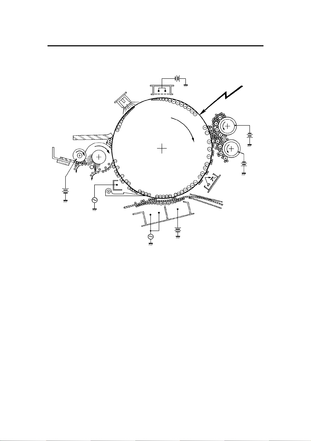
2. DRUM PROCESSES
8
1
2
9
3
4
7
5
6
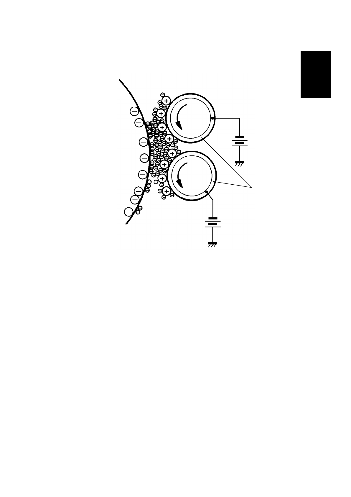
1. Charge
In the dark the charge corona unit applies a negative charge to the drum.
The grid plate ensures that the charge is applied uniformly. The charge
remains on the surface of the drum because the photoconductive drum has a
high electrical resistance in the dark.
2. Laser Exposure
A laser beam exposes the drum, forming an electrical latent image on the
drum surface.
3. Development
The magnetic developer brush on the development rollers comes in contact
with the latent image on the drum surface. Toner particles are
electrostatically attracted to the areas of the drum surface where the laser
reduced the negative charge on the drum.
1-6
Page 8

Overall
Information
1 February 1994 DRUM PROCESSES
4. Image Density Detection
On every 10th copy cycle, the laser forms a sensor pattern on the drum
surface. The ID sensor measures the reflectivity of the pattern. When the
image density of the pattern becomes too low, toner is supplied to the
development unit.
5. Image Transfer
Copy paper is fed to the drum surface while a positive charge is applied to
the back side of the paper. The positive charge pulls the toner particles from
the drum surface onto the paper.
6. Paper Separation
A strong ac corona discharge is applied to the back side of the copy paper,
reducing the charge on the paper and breaking the electrostatic attraction
between the paper and the drum. Then, the stiffness of the copy paper
causes it to separate from the drum. The pick-off pawls help to separate
paper which has low stiffness.
7. Pre-cleaning Corona (PCC)
The PCC applies a strong ac corona discharge to the drum. This completely
discharges the positive potential applied to the non-paper areas of the drum
at the transfer section. The PCC has a negative bias which increases the
negative charge on the toner remaining on the drum. This makes it easier for
the cleaning brush to remove the toner from the drum surface.
8. Cleaning
The cleaning brush and cleaning blade remove any toner remaining on the
drum surface. The cleaning brush is conductive and receives a positive
charge from the bias roller (to which +150 Vdc is applied). This helps it to
clean the negatively charged toner from the drum. The bias roller and a
beater bar remove the toner from the cleaning brush.
9. Quenching
The light from the quenching lamp electrically neutralizes the surface of the
drum.
1-7
Page 9
COPY PROCESS 1 February 1994
3. COPY PROCESS
This section gives an overview of the copy process used in this machine. For
more details, see the appropriate section description in the second chapter.
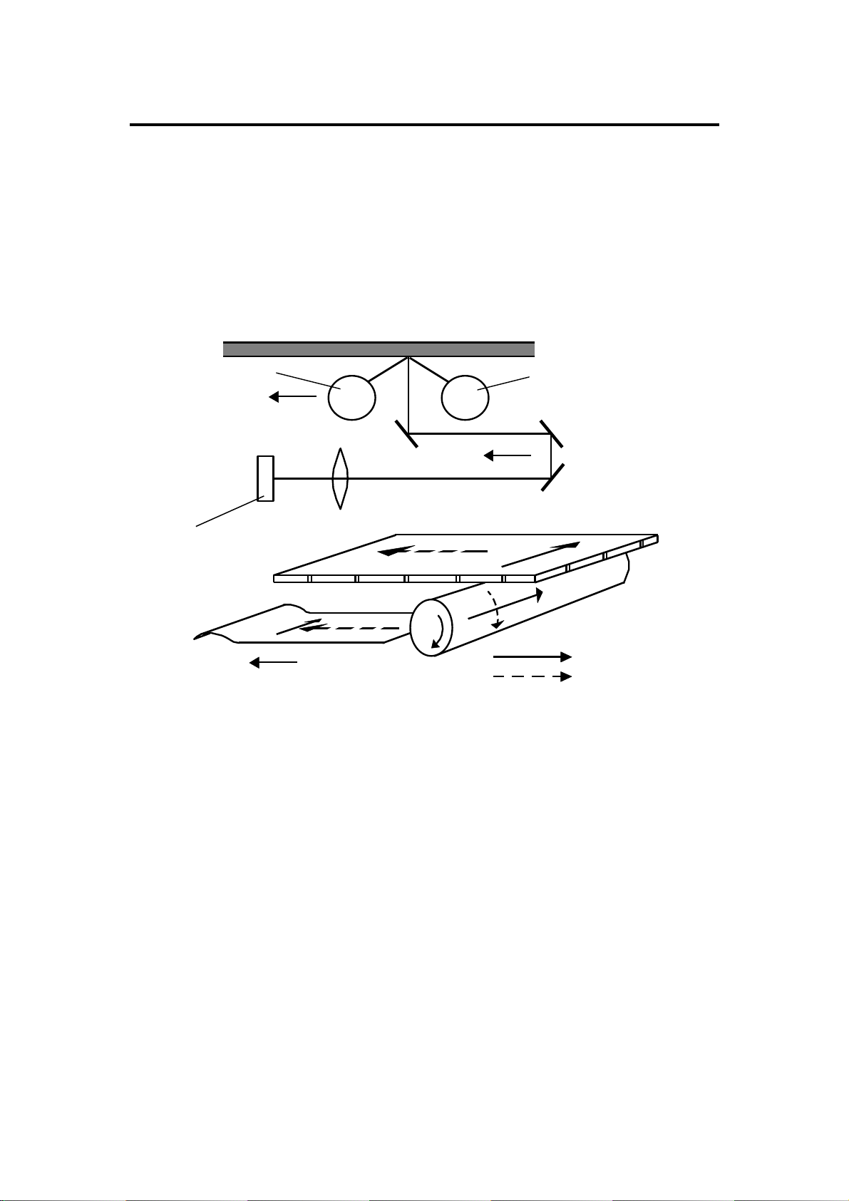
3.1 SCANNING AND IMAGE PROCESSING
3.1.1 Original Scanning
[A]
[A]
[B]
Main Scan
Sub Scan
The scanner lamps [A] expose the original as in a normal copier. However,
the optical system directs the light to the CCD [B] (charge coupled device)
rather than a drum or OPC belt. The CCD converts the light intensity to
electrical charges.
In this machine, the "main scan" direction refers to the direction perpendicular
to scanner and paper travel. The "sub scan" direction is the direction of
scanner movement, paper movement, and drum rotation.
1-8
Page 10
Overall
Information
1 February 1994 COPY PROCESS
3.1.2 Photoelectric Conversion
The CCD contains 5,000 picture elements (pixels) in a line (400
dots/inch, 15.7 dots/mm). It converts
the original light intensity into an
electrical signal (analog).
Voltage
2
CCD
Output
Main
Scan
White
3.1.3 Analog to Digital Conversion
The analog signal output from the
CCD is digitized. Eight bits are used
for each pixel (picture element)
which gives 256 gradation steps
(256 level grayscale).
3.1.4 Image Processing
The digitized signal is then processed to convert the 8-bit grayscale
image to 4-bit data which the laser
unit can print (16 level grayscale).
The image is processed in one or
more of the following ways:
• Main scan magnification (sub
scan magnification is changed
by varying the scanner speed)
8-Bit
Data
4-Bit
Data
Black
Analog
0 5000
27
26
25
24
23
22
21
2
1
0 81 82 83 84 85 86 87 88 89 90 91 92 93 94 95
CCD Element
A/D Conversion
8 bits/256 graduation
(Digital)
(F)
Black
Voltage
0.84
0.81
0.78
0.75
0.72
0.69
0.63
5000
: CCD Output
: 8-Bit Digital
• Letter mode (line image) or
photo mode processing
(8)
• Identification of designated areas
• Double copy image processing
White
(0)
GrayWhite Black
1-9
Page 11
COPY PROCESS 1 February 1994
3.2 DRUM EXPOSURE
A semiconductor laser exposes the
drum. The laser is switched on and
off at a very high frequency according to the image signal. Where the
laser beam strikes the drum, the
negative charge (about --850 volts)
on the drum drops (to about --100
volts), forming an electrical latent
image on the drum surface.
5
4
3
2
1
3’
2’
1’
Pitch
1/400"
(63.5
The laser beam is reflected by a
turning polygon mirror. The light
passes through a complex lens
(called the f
Θ lens) to the drum.
Main scanning (or in this case writing) is from front to rear, and one
surface of the polygon mirror is used
for each line.
µ)
Polygon
Mirror
Pitch 1/400" (63.5µ)
1 2 3 4 5 6 7
Mainscan
fΘ Lens
Laser
Drive
4’
3’
2’
1’
Subscan
R
Drum
F
1-10
OFFONOFF
--850 V
Mainscan
Page 12
Overall
Information
1 February 1994 COPY PROCESS
3.3 DEVELOPMENT PROCESS
[A]
[B]
A: OPC Drum
B: Development Roller
Most copiers use either a positively charged photoconductor and negatively
charged toner or a negatively charged photoconductor and positively charged
toner. This is known of as positive/negative development. However, this
machine uses a negative/negative process where both the drum surface
charge and the toner charge are negative. The negative/negative process
has certain advantages for laser printing, but some copy problems are
exactly opposite from what many copier service people have intuitively come
to expect. The table on the following page gives some of the differences
between the positive/negative process and the negative/negative process.
1-11
Page 13
COPY PROCESS 1 February 1994
Positive/Negative Development VS. Negative/Negative Development
(2- component dry development process)
Positive/Negative Negative/Negative
Type of Laser He-neon (gas,
630 nm)
Photoconductor Se Drum OPC OPC
Charge Corona Positive Negative Negative
Carrier Charge Positive Negative Positive
Toner Charge Negative Positive Negative
Photoconductor
Exposure
Background exposure (write to
white)
He-neon or
semiconductor
Semiconductor (780 nm)
Image exposure (write to black)
P: Pitch (1/400"
in this model)
D: Laser beam
diameter
V
D: Drum voltage
V
B: Bias voltage
V
R: Residual
voltage L1, L2: Line
width (L1 < L2 for
the same laser
beam diameter)
Copy Problems
1. No
photoconductor
charge
2. Low
photoconductor
charge
3. High
development bias
4. Low development
bias
5. Stained toner
shield glass
P
D
V
V
0V
P
B
R
P
D
V
L1
P
White copy Black solid copy
Low image density Dirty background
Low image density Dirty background
Dirty background Low image density
Black stripes White stripes
V
D
B
V
R
V
0V
L2
1-12
Page 14
Overall
Information
1 February 1994 MECHANICAL COMPONENT LAYOUT
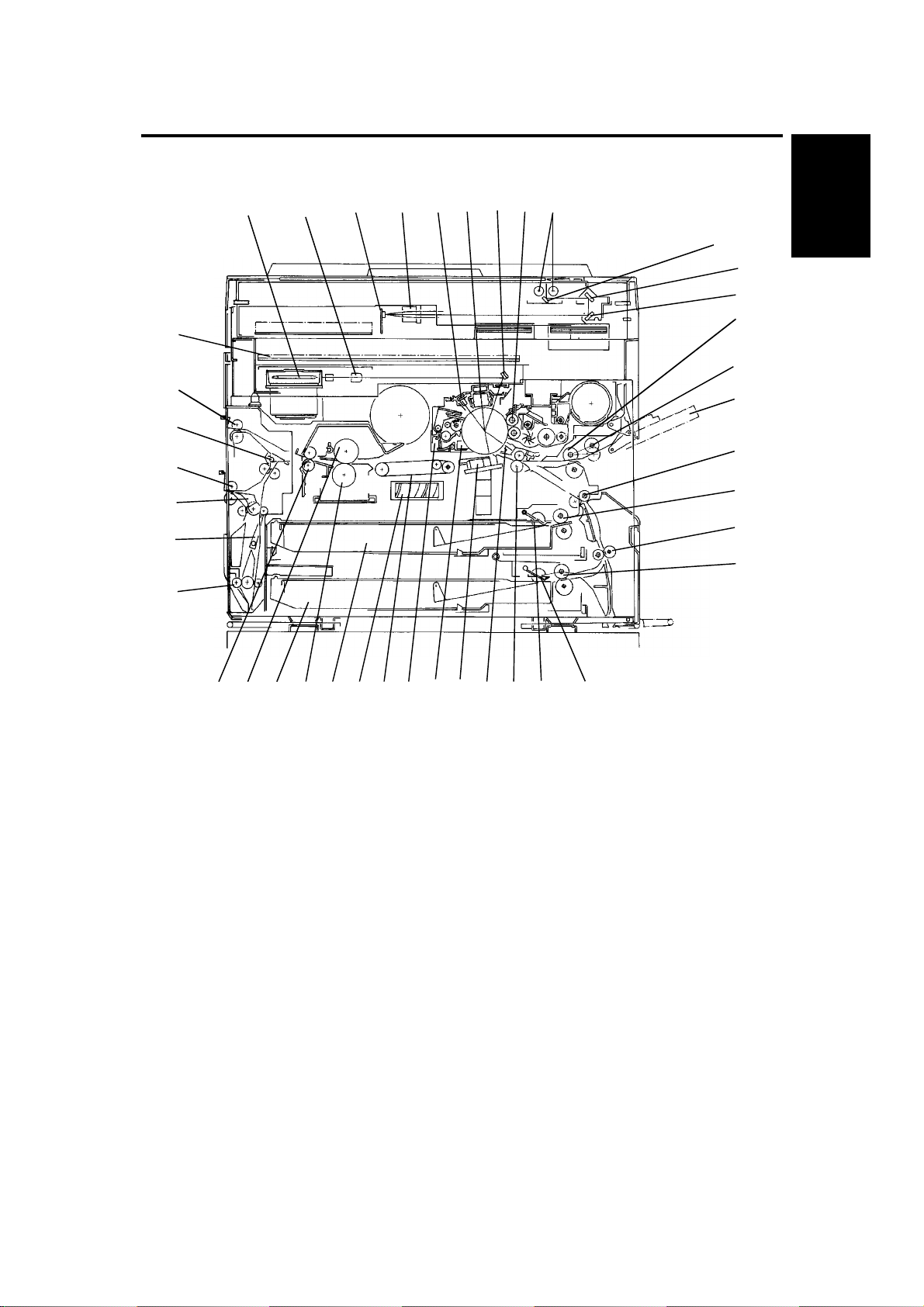
4. MECHANICAL COMPONENT LAYOUT
40
39
38
37
36
35
34
1 2 3 4 5 6 7 8 9
10
11
12
13
14
15
16
17
18
19
33 32 31 30 29 28 27 26 25 24 23 22 21 20
1. Polygon Mirror Motor
2. F
θ Lens
3. Sensor Board Unit (SBU)
4. Lens
5. Quenching Lamp
6. Charge Corona Unit
7. Drum Mirror
8. Development Rollers
9. Exposure Lamps
10. First Mirror
11. Second Mirror
12. Third Mirror
13. Side Paper Feed Roller
14. Side Pick-up Roller
15. Multi By-pass Tray
16. First Relay Roller
17. First Paper Feed Roller
18. Second Relay Roller
19. Second Paper Feed Roller
20. Second Pick-up Roller
21. First Pick-up Roller
22. Registration Rollers
23. Image Density Sensor
24. Transfer/Separation Corona Unit
25. Pre-Cleaning Corona Unit
26. Cleaning Unit
27. Transport Belt
28. Vacuum Fan
29. First Cassette
30. Pressure Roller
31. Second Cassette
32. Hot Roller
33. Fusing Exit Roller
34. Return Pinch Roller
35. Return Gate
36. Inverter Entrance Gate
37. Lower Exit Rollers
38. Junction Gate
39. Upper Exit Rollers
40. Printer Control Board
1-13
Page 15
DRIVE LAYOUT 1 February 1994
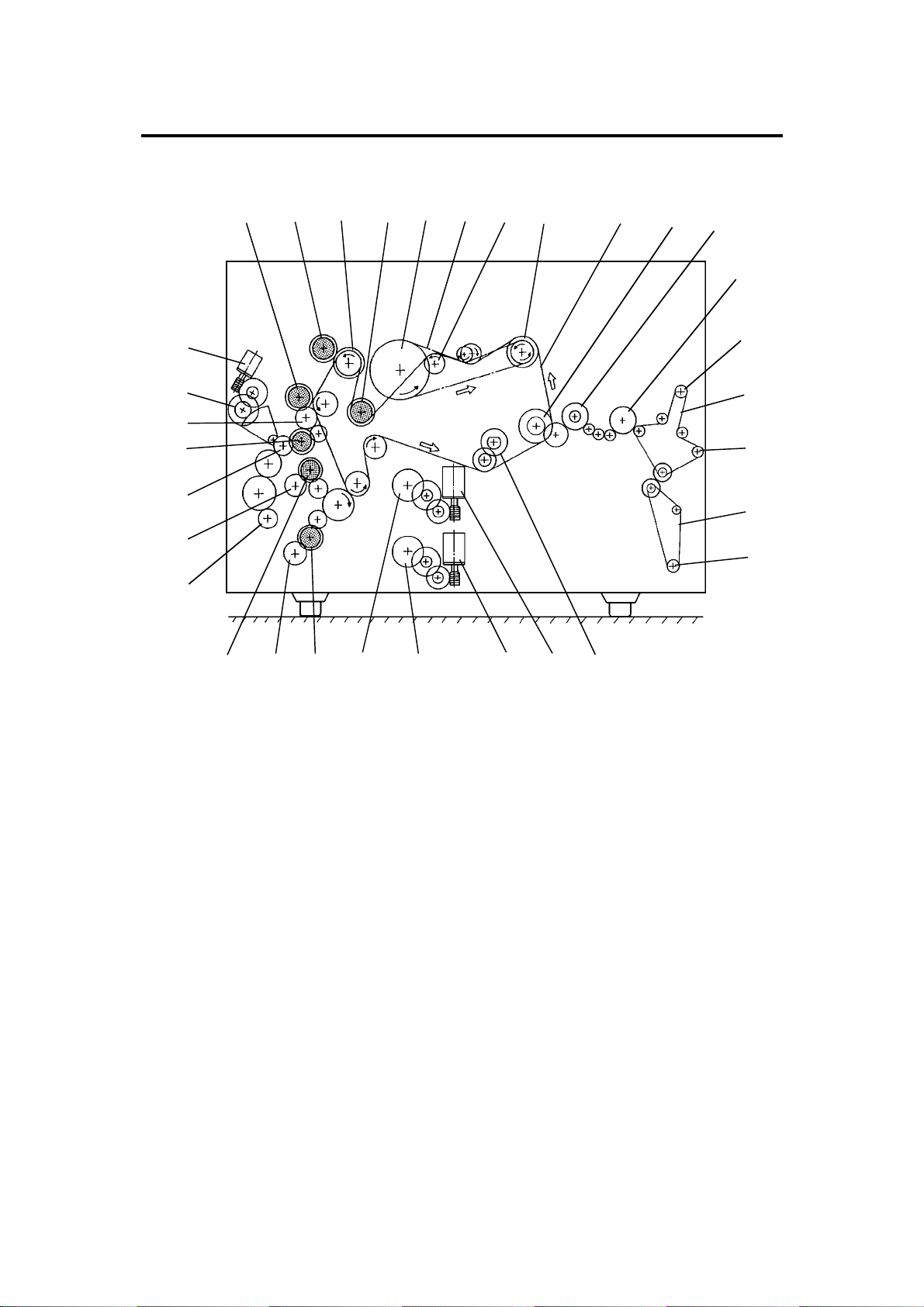
5. DRIVE LAYOUT
32
31
30
29
28
27
26
1 2 3
4 5
6 7 8
9
10
11
12
13
14
15
16
17
25
1. Side Paper Feed Clutch
2. Toner Supply Clutch
3. Development Clutch
4. Registration Clutch
5. Drum Drive Gear
6. Drum Drive Belt
7. Cleaning Drive Gear
8. Main Motor Gear
9. Main Drive Chain
10. Fusing Drive Gear
11. Hot Roller Drive Gear
12. Inverter Unit Drive Gear
13. Upper Exit Roller Gear
14. Exit Roller Drive Belt
15. Lower Exit Roller Gear
16. Reverse Pinch Roller Drive Belt
24 23
22
21
20
17. Reverse Pinch Roller Gear
18. Used Toner Tank Drive Gear
19. First Paper Lift Motor
20. Second Paper Lift Motor
21. Second Paper Lift Gear
22. First Paper Lift Gear
23. Second Paper Lift Gear
24. Second Separation Roller Gear
25. First Paper Feed Clutch
26. Second Relay Roller gear
27. First Separation Roller Gear
28. First Relay Roller Gear
29. Relay Clutch
30. Side Separation Roller Gear
31. Side Paper Lift Gear
32. Side Paper Lift Motor
19 18
1-14
Page 16

Overall
Information
1 February 1994 ELECTRICAL COMPONENT DESCRIPTIONS
6. ELECTRICAL COMPONENT DESCRIPTIONS
SYMBOL NAME FUNCTION INDEX NO.
Motors
M1 Main Motor Drives all the main unit components except for
the optics unit and fans.
M2 Scanner Motor Drives the scanner. 21
M3 Side Paper Lift
Motor
M4 1st Paper Lift
Motor
M5 2nd Paper Lift
Motor
M6 Polygon Mirror
Motor
M7 Optics Cooling
Fan Motor
M8 Exhaust Fan
Motor
M9 Printer Controller
Fan Motor
M10 Printer Controller
Cooling Fan
Motor
M11 Charge Fan
Motor
M12 Vacuum Fan
Motor
M13 LD Cooling Fan
Motor
Lifts the side cassette’s bottom plate. 15
Lifts the 1st cassette’s bottom plate. 9
Lifts the 2nd cassette’s bottom plate. 8
Turns the polygon mirror. 4
Cools the optics cavity. 3
Removes the air around the transport and the
fusing unit.
Removes the air around the printer I/F board. 2
Cools the printer I/F board area. 19
Provides a flow of air to the charge corona unit
to prevent uneven charge.
Provides suction so that paper is held firmly on
the transport belt.
Cools the LD driver board area. 6
18
1
16
7
Magnetic Clutches
MC1 Registration
Clutch
MC2 Side Paper Feed
Clutch
MC3 Relay Roller
Clutch
MC4 1st Paper Feed
Clutch
MC5 2nd Paper Feed
Clutch
MC6 Development
Clutch
Solenoids
SOL1 Toner Supply
Solenoid
Turns the registration rollers. 10
Starts paper feed from the side feed station. 14
Turns the relay rollers. 13
Starts paper feed from the first feed station. 12
Starts paper feed from the second feed station. 11
Transmits the main motor drive to the
development drive gears.
Turns on to supply toner to the development
unit.
1-15
17
99
Page 17

ELECTRICAL COMPONENT DESCRIPTIONS 1 February 1994
SYMBOL NAME FUNCTION INDEX NO.
SOL2 Cleaning
Solenoid
SOL3 Side Pick-up
Solenoid
SOL4 1st Tray Lock
Solenoid
SOL5 2nd Tray Lock
Solenoid
SOL6 2nd Pick-up
Solenoid
SOL7 1st Pick-up
Solenoid
SOL8 Return Pinch
Roller Solenoid
SOL9 Junction Gate
Solenoid
SOL10 Inverter
Entrance
Solenoid
Presses the cleaning blade against the drum. 98
Controls the up-down movement of the side
pick-up roller.
Locks the first tray during coping cycle. 96
Locks the second tray during coping cycle. 95
Controls the up-down movement of the second
pick-up roller.
Controls the up-down movement of the first
pick-up roller.
Opens the return gate and presses the return
pinch roller against the return roller.
Opens the junction gate. 23
Opens the inverter entrance gate. 24
97
94
93
64
Switches
SW1 Main Switch Provides the power to the copier. 35
SW2 Front Door
Safety Switches
SW3 Anti-
condensation
Switch
SW4 Function Switch Provides the power to the printer I/F board. 36
SW5 Right Upper
Door Switch
SW6 Left Upper Door
Switch
Sensors
S1 Scanner H.P.
Sensor
S2 Scanner Unit Lift
Sensor
S3 Original Length
Sensor
S4 Original Width
Sensor 1
S5 Original Width
Sensor 2
S6 Platen Cover
Position Sensor
S7 Manual Feed
Width Sensor
Cuts dc power and the +5 volts for the laser
operation when the front cover is opened.
Cuts the power to the tray and lamp heaters,
drum heater, and the anti-condensation heater
when the switch turns off.
Detects when the right upper door is opened. 54
Detects when the left upper door is opened. 25
Notifies the CPU when the scanner is at the
home position.
Notifies the CPU when the scanner unit is
closed.
Detects the original length. 29
Detects the original width. 66
Detects the original width. 67
Gives the signal to perform original size
detection with open platen cover condition.
Informs the CPU of the width of paper which is
in the multi by-pass tray.
38
32
62
63
65
57
1-16
Page 18

Overall
Information
1 February 1994 ELECTRICAL COMPONENT DESCRIPTIONS
SYMBOL NAME FUNCTION INDEX NO.
S8 Side Paper Lift
Sensor
S9 Side Paper Size
Sensor
S10 1st Upper Limit
Sensor
S11 2nd Upper Limit
Sensor
S12 Manual Feed
Sensor
S13 Oil End Sensor Detects when it is time to add silicone oil. 37
S14 1st Paper Set
Sensor
S15 2nd Paper Set
Sensor
S16 1st Lower Limit
Sensor
S17 2nd Lower Limit
Sensor
S18 1st Relay Sensor Detects misfeeds. 49
S19 2nd Relay
Sensor
S20 Side Relay
Sensor
S21 2nd Paper End
Sensor
S22 1st Paper End
Sensor
S23 2nd Paper Size
Sensor
S24 1st Paper Size
Sensor
S25 Registration
Sensor
S26 ID Sensor Detects the density of the image on the drum. 40
S27 Fusing Exit
Sensor
S28 Platen Cover
Sensor
S29 Side Paper End
Sensor
S30 Toner Overflow
Sensor
S31 Upper Exit
Sensor
Detects the correct feed height of the side
cassette.
Informs the CPU what size paper is in the side
cassette.
Detects the correct feed height of the first
cassette.
Detects the correct feed height of the second
cassette.
Detects whether or not the manual feed table is
in the down position.
Detects whether or not the first paper tray is in
the main frame.
Detects whether or not the second paper tray
is in the main frame.
Detects the bottom plate of the first cassette is
in the down position.
Detects the bottom plate of the second
cassette is in the down position.
Detects misfeeds. 48
Detects misfeeds. 47
Informs the CPU when the second cassette
runs out of paper.
Informs the CPU when the first cassette runs
out of paper.
Informs the CPU what size paper is in the
second cassette.
Informs the CPU what size paper is in the first
cassette.
Detects misfeeds. 41
Detects misfeeds. 34
Detects when the platen cover or the DF is
closed, and gives the signal to perform original
size detection with closed platen cover
condition.
Informs the CPU when the side cassette runs
out of paper.
Detects when the used toner tank is full. 39
Detects misfeeds. 28
59
58
56
55
60
53
50
52
51
46
45
43
42
31
44
1-17
Page 19

ELECTRICAL COMPONENT DESCRIPTIONS 1 February 1994
SYMBOL NAME FUNCTION INDEX NO.
S32 Lower Exit
Sensor
S33 Inverter
Entrance Sensor
PCBs
PCB1 Main PCB Controls all copier functions both directly and
PCB2 AC Drive PCB Provides ac power to the fusing lamp. 76
PCB3 DC Drive PCB Drives the dc components such as the
PCB4 Operation Panel
PCB Unit
PCB5 Sensor Board
Unit (SBU) PCB
PCB6 Video
Processing Unit
(VPU) PCB
PCB7 Main Motor
Control PCB
PCB8 Image
Processing Unit
(IPU) PCB
PCB9 Laser Diode
(LD) Drive PCB
PCB10 Pulse Width
Modulation
(PWM) Control
PCB
PCB11 Printer Power
Supply PCB
PCB12 Printer Control
PCB
PCB13 Printer I/F Board
PCB
PCB14 Polygon Mirror
Motor Drive PCB
PCB15 Scanner I/F
Board PCB
(Option)
PCB16 DC Power
Supply PCB
PCB17 Inverter Drive
Board PCB
Detects misfeeds. 30
Detects misfeeds. 26
78
through other PCBs.
77
solenoids and sensors.
The user controls the machine through this
PCB.
Digitizes the original image as it is scanned. 75
Processes video read in through the SBU. 70
Controls the main motor. 20
Processes image read in through the VPU. 69
Controls the laser diode. 71
Provides the pulse to the other PCBs and
components.
Provides the power for the printer I/F board. 68
Controls the printer functions. 81
Connects the interface harnesses for the
printer.
Controls the polygon mirror motor. 5
Connects the interface harnesses for the
scanner.
Provides dc power to the copier. 102
Controls the inverter unit. 27
73
72
79
80
Lamps
L1 Exposure Lamp Provides light to reflect the original’s image
onto the SBU.
1-18
104
Page 20

Overall
Information
1 February 1994 ELECTRICAL COMPONENT DESCRIPTIONS
SYMBOL NAME FUNCTION INDEX NO.
L2 Quenching Lamp Neutralizes any charge remaining on the drum
surface after cleaning.
L3 Fusing Lamp Provides heat to the hot roller. 86
Power Packs
PP1 Transfer/
Separation
Power Pack
PP2 C/G/B/BR Power
Pack
Heaters
H1 Anticondensation
Heater
H2 Tray Heater Prevents moisture from forming inside the
H3 Lamp Heater Warms the exposure lamp. 103
H4 Drum Heater Keeps the drum warm to prevent condensation
Provides high voltage power for the transfer
corona, pre-cleaning corona and the
separation corona.
Provides high voltage power for the charge
corona wire, development bias, grid bias and
cleaning bias.
Prevents moisture from condensing on the
optics.
copier.
on the drum.
74
92
100
101
89
90
Counters
CO1 Total Counter Counts the number of pages in copy and print
mode.
CO2 Print Counter Counts the number of pages in print mode. 84
CO3 Key Counter
(Option)
Others
TH Thermistor Senses the temperature of the hot roller. 87
TF Thermofuse Opens the fusing lamp circuit if the fusing unit
NF Noise Filter Removes electrical noise from the AC input
CB Circuit Breaker Guards against voltage surges in the AC input
LS Lamp Stabilizer Powers the exposure lamps. 82
SMD Scanner Motor
Driver
HDD Hard Disk Unit
(Option)
Used for control of authorized use. Copier will
not operate until activated.
overheats.
line.
line.
Controls the scanner motor. 22
Stores the fonts for printer. 61
83
91
85
88
33
1-19
Page 21

SECTION 2
DETAILED SECTION
DESCRIPTIONS
Page 22

1 February 1994 DRUM
1. DRUM
1.1 DRUM CHARACTERISTICS
The organic photoconductor (OPC) drum has the following characteristics:
• It is able to accept a high negative electrical charge in the dark. (The
electrical resistance of the OPC drum is high in the absence of light.)
• The electric charge on the drum surface dissipates when the drum is
exposed to light. (The conductivity of the OPC drum is greatly enhanced
by exposure to light.)
• The OPC drum used in this machine is specially made for use with diode
lasers. It responds well to the 780 nm wavelength light of the laser used in
this machine.
Detailed
Descriptions
2-1
Page 23
DRUM 1 February 1994
1.2 DRUM DRIVE
[B]
[A]
[C]
The main motor turns the drum drive shaft [A] through the timing belt [B]. A
drive pin [C] on the end of the drum drive shaft fits into slots in the end of the
drum. This pin turns the drum whenever the main motor is on.
2-2
Page 24
1 February 1994 CHARGE
2. CHARGE
2.1 OVERVIEW
[A]
[P1]
Detailed
Descriptions
[C]
[D]
[B]
C/G/B/BR
P.P.
[C]
[D]
[B]
This model uses a dual wire corona unit [A] to charge the OPC (organic
photoconductor) drum [B]. The corona wire [C] generates a corona of
negative ions when a high negative voltage is applied to it by the charge/grid/
bias/bias roller power pack. To make the negative corona uniform, a thin
stainless steel grid [D] is installed on the charge corona unit. The drum
receives a charge of approximately --850 volts.
2-3
Page 25
CHARGE 1 February 1994
2.2 CHARGE VENTILATION
[A]
[B]
[C]
Ozone from the charge corona unit can oxidize the surface of the drum. This
oxidization can cause dirty background. To prevent this, the charge fan [A]
circulates air through the charge corona unit [B]. The airflow from this fan is
also directed to the auto image density sensor [C]. This helps to prevent
toner from settling on the auto ID sensor.
The charge fan turns on and off at the same time as the main motor.
2-4
Page 26
1 February 1994 CHARGE
2.3 CORONA WIRE CLEANER
[A]
[B]
Detailed
Descriptions
Toner particles or paper dust may be deposited on the corona wire by the air
flow around the charge corona unit. Such particles may interfere with
charging and cause dark lines on copies. The wire cleaner [A] allows the
operator to correct this problem by pulling out and pushing in the charge
corona unit.
When the corona unit is seated, the cleaning pads are held away from the
corona wire as shown in the illustration. However, when the charge corona
unit is pulled out, the wire casing [B] pushes the cleaning pads against the
wire as shown in illustration.
2-5
Page 27
CHARGE 1 February 1994
2.4 CHARGE CORONA CIRCUIT
Main Board
C-Trigger
G-Trigger
G-PWM
GND-Vcc
Grid voltage
(kV)
-0.5
-0.6
-0.7
-0.8
-0.9
-1.0
0
CN156
CN511
-A6
-A7
-A2
-A1
CN510
+24V (V )
AA
GND
20 40 60 80 100 (%)
PWM Duty
-4
-3
-8
-9
-1
-3
G-PWM
C/G/B/BR Power Pack
5
Charge
5
5
0
Grid
24
0
H
L
0
t2
t1
Charge
PWM Duty =
t1 = 1 ms
t2 = 0 ∼ 1 ms
Grid
t2
x 100 (%)
t1
The dc power supply board provides +24 volts (VAA) to the C/G/B/BR power
pack. The CPU drops CN156-A6 and -A7 from +5 volts to 0 volt. These are
the trigger signals for the high voltage power to the charge corona wire
(approx. --6.5 kV) and the grid wire (approx. --0.87 kV). The actual charge
applied to the OPC drum is approximately --850 volts.
<PWM (Pulse Width Modulation) Control>
Instead of a variable resister, the PWM control is used for the grid voltage.
The output level of the grid voltage increases as the duty of the G-PWM
signal increases as shown above.
The grid bias can be set by the SP2-1-1 (Grid Bias Adjustment).
2-6
Page 28
1 February 1994 SCANNING
3. SCANNING
3.1 OVERVIEW
[E]
[A]
[G]
[C]
Detailed
Descriptions
[F]
During scanning an image of the original is reflected on the CCD (charge
coupled device) of the SBU (sensor board unit) via the optics assembly as
follows:
Scanner Lamp [A] ⇒ Original ⇒ First Mirror [B] ⇒ Second Mirror [C]
⇒ Third Mirror [D] ⇒ Lens [E] ⇒ CCD (on SBU) [F]
Light from a band across the entire width (main scanning direction) of the
document is focused on the CCD by the lens (1 : 0.1102 ratio). The CCD has
5,000 picture elements which convert the light intensity into electric charges.
The image reading plate on the VPU converts the CCD charges into a 8-bit
(256 gradations) digital signal. 2835 lines are digitized per second.
The scanning resolution is 400 dpi (15.7 dots/mm) in the main scanning
direction. In full size mode it is also 400 dpi in the sub scanning direction.
(The scanner speed is 180 mm/s when in full size mode.)
[B]
[H]
[D]
The white plate [G] is scanned prior to scanning the original. This gives a
consistent white value which is used as a reference value to correct for
variations in the fluorescent lamp or irregularities in the light striking the CCD.
The anti-condensation heater [H] keeps moisture from forming inside the
scanner unit.
2-7
Page 29
SCANNING 1 February 1994
3.2 SCANNER LAMP
[B]
[A]
[C]
[D]
[E]
(without lamp grid) (with lamp grid)
The scanner lamps [A] are green fluorescent lamps with apertures so that
most of the light is output in a single direction. They are controlled by the IPU
board [B]. The scanner lamp stabilizer [C] drives the lamps with 15 W, 50 kHz
power. The high frequency is necessary to achieve an even supply of light to
the CCD, because the time for charging the CCD is 0.5 msec.
The scanner lamp heaters [D] keep the scanner lamp’s temperature at 40°C.
This is necessary because the light intensity will be insufficient if the scanner
lamp’s temperature is too low.
To prevent the light from being diffused, the lamp grid [E] is installed above
the lamps. This grid can minimize the flare as shown the above illustration.
2-8
Page 30
1 February 1994 SCANNING
3.3 SCANNER LAMP CIRCUIT
Lamp Heater
Thermistor
Lamp Heater
Scanner Lamp
2
1
2
1
1
CN657-4
2
1
2
-3
-2
-1
-10
-9
-8
-7
CN656-3
-2
-1
Lamp
Stabilizer
CN305-14
-13
-12
-11
CN305-7
-6
-5
[5] Vcc
[0--5] Thermistor
[▼24] Lamp Heater
[24] VAA
[0] G.VAA(INV)
[24] VAA
[▼24] FLON
IPU Board
Detailed
Descriptions
The scanner lamp stabilizer is powered by +24 volts from CN305-6. To turn
on the scanner lamp, the IPU board drops CN305-5 to Low. The scanner
lamp stabilizer then provides high frequency power to the filaments of the
scanner lamp.
The IPU board monitors the temperature of the scanner lamps through the
lamp thermistor, and turns the scanner lamp heaters on and off to keep the
scanner lamps at 40°C. It generally takes about 1 minute for the scanner
lamps to reach 40°C after the main switch is turned on.
2-9
Page 31

SCANNING 1 February 1994
3.4 SCANNER DRIVE
[D]
[E]
[A]
[B]
[C]
This model uses a dc servomotor [A] to drive the scanners.
The first scanner [B] consists of the scanner lamps and the first mirror, and
the second scanner [C] consists of the second and third mirrors. Unlike most
conventional copiers, four drive wires move these scanners. Four wires are
used to keep scanner movement very smooth.
The rear wire clamp [D] of the first scanner also works as the actuator of the
scanner home position sensor [E].
2-10
Page 32

1 February 1994 SCANNING
3.5 SCANNER DRIVE CIRCUIT
IPU Board
Vcc [5]
ECA
ECB
GND [0]
REVTTL
DGND
FWDTTL
DGND
REVOC
DGND
FWDOC
DGND
SHORT
DGND
GND [0]
H.P. Sensor [▲5]
Vcc [5]
Scanner
Unit Lift Sensor [▲5]
Vcc [5]
GND [0]
Feed-back
CN303-1
-2
-3
-4
CN302-1
-2
-3
-4
-5
-6
-7
-8
-9
-10
CN305-10
-9
-8
CN318-1
-8
-3
Encoder
Speed/Direction control
H.P. Sensor
Scanner Unit
Lift Sensor
Scanner
Drive Motor
Power
CN331-1
CN332-1
-10
Motor Drive
Board
[▲24V] FWD
-2
[▲24V] REV
-3
[0] GND
REVTTL
-2
DGND
-3
FWDTTL
-4
DGND
-5
REVOC
-6
DGND
-7
FWDOC
-8
DGND
-9
SHORT
DGND
Detailed
Descriptions
Unlike most conventional copiers, two PCBs are used to operate the scanner
drive motor. The IPU board receives the feed-back data for the motor speed
and the direction from the motor encoder and then, sends the control signal
to the motor drive board. In accordance with these control signals, the motor
drive board supplies the power, so that the scanner drive motor rotates at the
proper speed and direction.
By keeping the control signal lines away from the power supply lines, the
influence of any electrical noise is minimized.
2-11
Page 33

SCANNING 1 February 1994
[B]
[A]
For field servicing, the scanner unit can be opened. When the scanner unit is
lifted, the actuator [A] of the scanner unit lift sensor [B] moves out of the
sensor (CN318-8 0 ⇒ 5 V).
Then, the CPU prohibits the scanner motor from rotating, for safety.
2-12
Page 34

1 February 1994 SCANNING
3.6 ORIGINAL SIZE DETECTION IN PLATEN MODE
[B]
[C]
[F]
Detailed
Descriptions
[A]
[G]
[D]
[E]
An original width sensors [A] and an original length sensor [B] are under the
exposure glass [C]. The original width sensor consists of four reflective
photosensors. The original length sensor consists of three reflective
photosensors.
While the main switch is on, these sensors are active and the IPU board
receives their output signals. The IPU board checks the output signals twice
as the platen cover (document feeder) is being closed.
The first check is done when the platen cover position sensor [D] turns on.
(When the document feeder is installed, the first check is done when the DF
position sensor [G] on the document feeder turns on.) The platen cover
position sensor is actuated when the platen cover (document feeder) is
lowered to about 10 cm (4") above the exposure glass. At this time only the
sensors located underneath the original receive the reflected light. These
sensors output LOW signals.
2-13
Page 35

SCANNING 1 February 1994
The second check is done when the platen cover closed switch [E] turns on.
This is when the platen cover (document feeder) is completely closed. The
platen cover closed switch is a reed switch. A magnet [F] mounted on the
platen cover (document feeder) actuates the reed switch.
The second check is necessary to confirm that the original size detected at
the first check is correct. This double check prevents original size detection
errors that may occur if a black solid area on the original is positioned directly
over a sensor.
When a copy is made with the platen cover (document feeder) open, the
CPU checks the original size when the Start key is pressed.
The following illustration shows the location of the original width and length
sensors. The table shows the sensor output (HIGH, LOW) for each original
size.
S1
S3
L1
L2
L3
S2
S4
Sensors
Original Size
11" x 17" A3 0 0 0 0 0 0 0
10" x 14" B4 1 0 0 0 0 0 0
1
8
⁄
" x 14" ---- 1 0 0 1 0 0 0
2
1
8
⁄
" x 11" A4 (L) 1 1 1 1 0 0 0
2
8" x 10" B5 (L) 1 1 1 1 1 0 0
11" x 8
5
8
1
⁄
" A4 (S) 1 1 1 0 0 0 0
2
1
1
⁄
" x 8
⁄
2
1
⁄
2
" A5 (L) 1 1 1 1 1 1 0
2
1
" x 5
⁄
" A5 (S) 1 1 1 1 1 0 1
2
---- F 1 1 0 1 1 0 0
Original Length Sensor Original Width Sensor
L1 L2 L3 S1 S2 S3 S4
0: LOW
1: HIGH
NOTE: In case of other combinations, the "Original Size not sensed" will be
indicated.
2-14
Page 36

1 February 1994 IMAGE PROCESSING
4. IMAGE PROCESSING
This section deals with the processing of scanner data from its generation by
the CCD until its output to the laser unit as serial data.
4.1 OVERVIEW
Detailed
Descriptions
SBU
VPU
C
C
D
Analog
8 bit
IPU
GATE ARRAY
1~6
MAIN PCB
4 bit 4 bit
Laser
Section
The CCD generates an analog video signal. The SBU then sends the analog
video signal to the VPU board.
The processing of the VPU (Video Processing Unit) includes signal
composition, variable amplification, and digitization.
The IPU (image processing unit) processes the 8-bit signal. This processing
includes several functions, for example, halftone imaging, MTF (modulation
transfer function) correction, and main scan magnification. The IPU
generates a 4-bit signal which is sent to the laser section through the main
PCB.
The main PCB sends the 4-bit signal to the laser section.
2-15
Page 37

IMAGE PROCESSING 1 February 1994
4.2 SENSOR BOARD UNIT
4.2.1 Basic Functions
Even
CCD
Reflected
light
Amplifier
ODD
Switching clock
Photoelectric
conversion
Signal
amplification
The illustration above shows the main elements of the SBU (sensor board
unit) in block form. The SBU performs the following functions:
Photoelectric conversion: The light reflected from the original is converted to
an analog signal. This is done by the CCD, which has 5,000 picture
elements. The resolution is 400 dots per inch (15.7 lines/mm).
Signal amplification: To speed up processing, odd and even pixels are read
from the CCD separately and then amplified.
2-16
Page 38

1 February 1994 IMAGE PROCESSING
4.2.2 SBU Circuit Operation
SBU: Sensor Board Unit
Lens
CCD
5000
12 V
1
2
3
OS1
OS2
AMP
AMP
VIDEO1
VIDEO2
GND
VPU
VPU
VPU
CCD: Charge Coupled Device
The SBU converts the light reflected from the document to two analog
signals. The following covers how the video data is changed at each step of
the process.
-- Photoelectric Conversion --
Detailed
Descriptions
The CCD elements convert the light from the image to an analog signal. To
increase the scanning speed, the CCD handles the odd pixel (picture
element) data and even pixel data separately. Odd data is output from OS1
and even data is output from OS2. After amplification, the wave form of these
signals is similar to the illustration on the next page. The timing of these
signals is as follows:
2-17
Page 39

IMAGE PROCESSING 1 February 1994
Main Scan 1 line
TG
O
/
O
/
O
/
OS
1
2
1OS
B1 B3
2
B2 B26 B28
B25 B27
B29
B30
D
U
M
M
Y
D
U
M
M
Y
3
1
2
5 4995
Odd video data
4
Even video data
4997
4996
4998
4999
5000
D
U
M
M
Y
D
U
M
M
Y
Clock
Video
Signal
O/ TG: Clock for main scan
O/ 1 and O/ 2: Clock pulses
OS1: Odd video data
OS2: Even video data
2-18
Page 40

1 February 1994 IMAGE PROCESSING
4.3 VIDEO PROCESSING UNIT
4.3.1 Basic Function
From
SBU
VPU (Video Processing Unit)
Amplifier
Amplifier
AGC data *
(4 bits)
From
IPU
Variable
amplification
Switching clock
Signal
composition
* AGC: Auto Gain Control
From
IPU
DA 01- DA 08
A/D
converter
AD clock
From
IPU
Signal
digitalization
8-bit data
To IPU
Detailed
Descriptions
The illustration above shows the main elements of the VPU (video
processing unit) in block form. The VPU performs the following functions:
Variable amplification: The pixels of the signal are amplified using the AGC
(auto gain control) signal. This is to compensate for variations in the light
source.
Signal composition: The odd and even signals are merged into a single video
signal.
Signal digitization: The analog signal is converted to an 8-bit digital signal
and then sent to the IPU.
2-19
Page 41

IMAGE PROCESSING 1 February 1994
4.3.2 VPU Circuit Operation
IPU
SBU
IPU
IPU
VPU: Video Processing Unit
12 V
VIDEO1
VIDEO2
-12 V
PWIND
AEMODE
SHADE
TP203
VR201
TP204
VR202
12 V
TP209
VR205
12 V
PEAK
HOLD
VR203
VR204
REF(+)
HC4066
A/D
MP7688
REF(-)
AUTO
GAIN
PXSW1
PXSW2
AGC1
AGC2
AGC3
AGC4
DB8
DB7
DB6
DB5
DB4
DB3
DB2
DB1
CLOCK
IPU
IPU
IPU
The VPU converts the analog video data from the SBU to an 8-bit digital
video data signal. The following covers how the video data is changed in
each step of the process.
-- Variable Amplification --
The video signals are adjusted by VR203 for odd pixel data and VR204 for
even pixel data and the auto gain control.
NOTE: VR203 and VR204 are used to adjust the overall video signal level.
100%
100%
80%
Too low
100%
Good level
TP209
Too big
2-20
Page 42

1 February 1994 IMAGE PROCESSING
-- Signal Composition --
The odd and even video signals are merged by IC HC4066.
HC4066
1 3 5 4995
2 4 4996
4997
4998
4999
5000
-- Auto Gain Control --
The video signal is modified by
AGC1 -- 4, supplied from the IPU.
This compensates for fluctuations
of the scanner lamp light level (due
to temperature and time). The gain
value is decided by scanning the
white plate prior to scanning the
original.
-- Signal Digitization --
3V
2
1
The wave form at TP209
3 4 4998
0.55 ms
4999
5000
Detailed
Descriptions
The adjusted video data goes to the A/D converter (MP7684), which converts
the serial video data to 8-bit digital data.
2-21
Page 43

IMAGE PROCESSING 1 February 1994
4.3.3 Auto Image Density Control
VIDEO PROCESSING UNIT (VPU)
Video
Auto ID Measuring Area
Peak
Hold
Vin
+Ref
-Ref
AEMODE
PWIND
Sub Scan
A/D
CN321
-53
-54
-55
-56
-57
-58
-59
-60
-39
-37
IMAGE PROCESSING
UNIT (IPU)
AGC
CN301
-53
-54
-55
-56
-57
-58
-59
-60
-39
-37
GA2
Main
Scan
64mm
8.3mm
1 to 3 mm
Unlike standard analog copiers, this machine does not prescan using an
image sensor to determine original image density. Instead, this machine
measures the background density of a 64 millimeter wide area of the
document continuously while the original is scanned. Data from the CCD is
used to check the background density, and the scanned data is made lighter
or darker by the A/D (analog/digital) converter in the VPU.
The scanned video data goes from the CCD to both the A/D converter and
the peak hold circuit. The peak hold circuit selects the peak voltage for each
line scanned and sends it as "+Ref" to the A/D converter. The "--Ref" input is
always 0 volts.
2-22
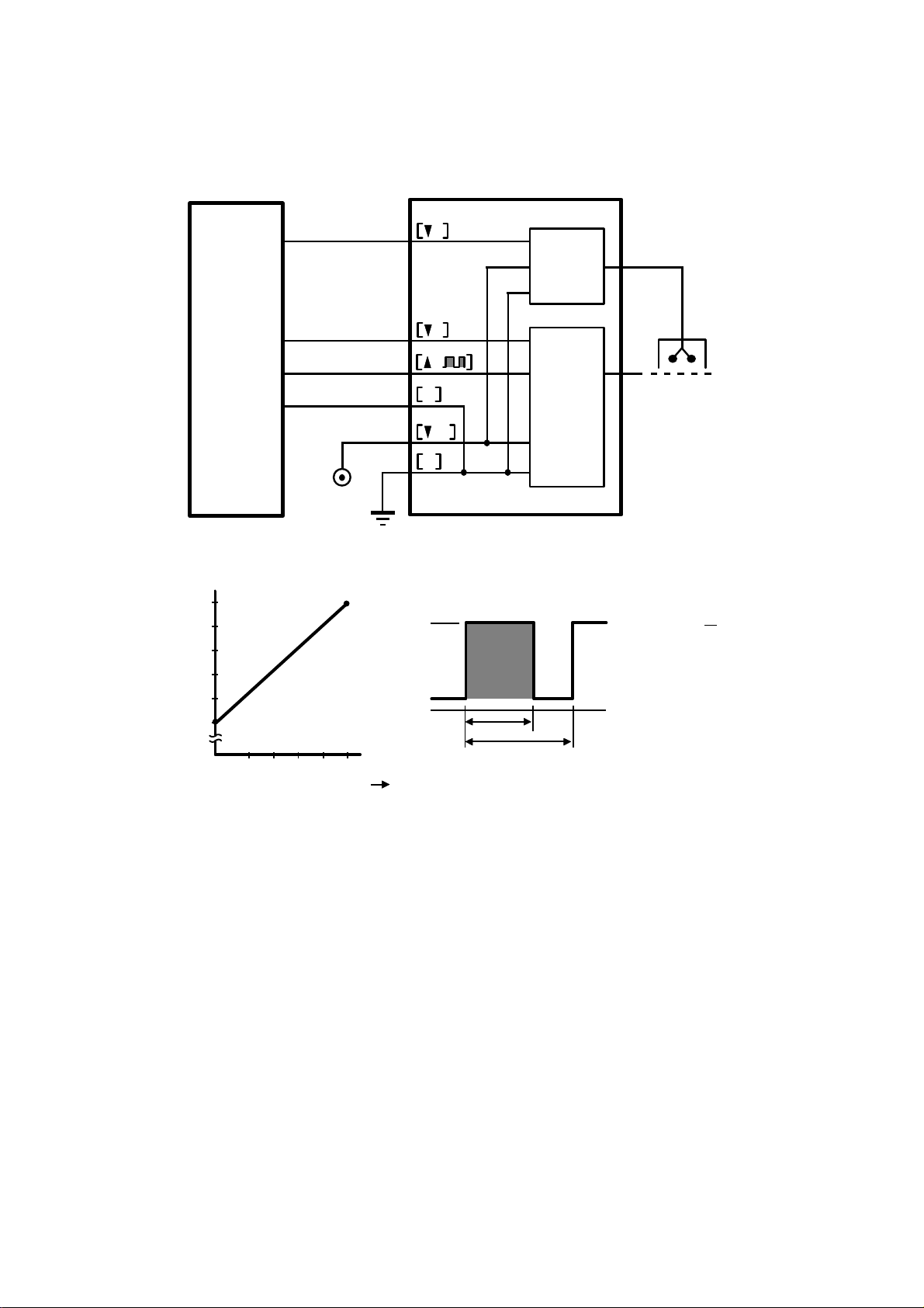
Page 44

1 February 1994 IMAGE PROCESSING
SFGATE
1 Line
LSYNC
AEMODE
PWIND
Auto image density measuring area
1 Page
To enable "+Ref", GA1 on the IPU sends 2 signals. One is AEMODE, which
goes to Low when the machine starts scanning and then goes High again
after scanning is complete. The other signal is PWIND, which is a pulse
signal which determines how wide the auto image density measuring area is.
This means the peak hold circuit functions only while PWIND is Low.
The A/D converter decides the appropriate video data based on both signals,
then digitizes the data signal.
Detailed
Descriptions
Analog Digital
White
Black
+Ref
Range
2.9 V
1.7 V
0 V
256
256
255
4
3
2
1
...........................
............................
............................
............................
............................
............................
............................
00000000
00000000
00000001
11111100
11111101
11111110
11111111
256 levels calculated
as follows:
D= Vin x
(D is the Digital data)
256
+Ref
+Ref can take values from +1.7 volts to +2.9 volts. The A/D converter divides
+Ref into 256 levels and digitizes the data signal (Vin) based on these levels.
The above chart shows how this is done.
2-23
Page 45

IMAGE PROCESSING 1 February 1994
Subscanning
Detection
Area
4
3
2
Sub-scanning
1
Reference
(+Ref)
2.9V
1.7V
0V
The reference value (+Ref) changes according to the image density in the
area measured. However, to prevent dirty backgrounds due to sudden
changes in the area sampled, the response to a light to dark change is
slower than the response to a dark to light change.
This is illustrated above. At point (1) where the sampled image changes from
black to white, +Ref changes to 2.9 volts immediately. At points (2), (3), and
(4), +Ref starts decreasing slowly, but it returns to 2.9 volts immediately as
soon as white is encountered in the detection area.
2-24
Page 46

1 February 1994 IMAGE PROCESSING
4.4 IMAGE PROCESSING UNIT
4.4.1 Basic Functions
Video Processing
Unit (VPU)
8-bit Video
AGC Reference
Timing
Image Processing Unit (IPU)
GA1
GA2
GA3
GA4
CPU
GA5
GA6
Drive
Timing
10-bit Data
Command
Main PCB
Thermister
Sensors
Motor
Lamp
Heater
Solenoid
Detailed
Descriptions
PROM
RAM
The IPU uses six gate arrays (custom made LSIs) to process the video data.
These gate arrays, which are labeled GA1 - GA6 in the above illustration,
have the following functions.
-- Gate Array 1 (GA1) --
Timing control and CCD drive clock
-- Gate Array 2 (GA2) --
Auto shading and Auto gain control (AGC)
-- Gate Array 3 (GA3) --
MTF (modulation transfer function) processing, Flare prevention and
Smoothing
2-25
Page 47

IMAGE PROCESSING 1 February 1994
-- Gate Array 4 (GA4) --
Main scanning magnification
-- Gate Array 5 (GA5) --
Gamma (γ) correction, Binary processing and 16 level grayscale processing
-- Gate Array 6 (GA6) --
Marker area detection, Background Numbering, Binary and 16 level
grayscale processing control
2-26
Page 48

1 February 1994 IMAGE PROCESSING
4.4.2 IPU Data Flow
VPU
8-bit Video Signal
Auto-shading
(GA2)
Letter Mode
Processing
MTF Correction
(GA3)
16 Level Grayscale
Processing
(GA5)
Magnification
Gamma Correction
Photo Mode
Processing
Smoothing
(GA3)
(GA4)
(GA5)
MTF Correction
(GA3)
Binary Processing
(GA5)
Letter/Photo
Mode Processing
Marker Area
(GA6)
Detailed
Descriptions
Image Editing
(GA6)
4-bit Video Signal (16 Level Grayscale Processing)
1-bit Video Signal (Binary Processing)
Main Board
The 8-bit video data from the VPU goes first to GA2 for auto-shading. The
corrected data then goes to GA3.
At GA3 data processing splits into letter mode processing, photo mode, and
letter/photo mode processing. For letter mode and letter/photo mode
processing, GA3 applies the MTF correction. For photo mode processing, it
applies a smoothing function.
Next the video data goes to GA4 where the magnification correction is
applied (if necessary).
After magnification, the data goes to GA5, where it is subjected to a gamma
correction. If the marker function is selected, the magnification processing
data goes to GA6, where the image data for marker area recognition is
produced. Then it goes to image editing.
2-27
Page 49

IMAGE PROCESSING 1 February 1994
If binary processing is selected, the magnification processing data goes to
the binary processing mode in GA5, where it is converted to a black and
white signal bit image.
If 16 level grayscale processing is selected, the gamma correction data goes
to the 16 level grayscale processing mode in GA5, where it is distributed over
16 levels.
16 level grayscale processing and binary processing can be chosen for each
original mode (letter, photo and letter/photo) through the SP4-403.
Finally, the output data from GA5 goes to the image editing section in GA6,
where background numbering and marker image data are processed. Then
the appropriate video data is ready for output to the main board.
2-28
Page 50

1 February 1994 IMAGE PROCESSING
4.4.3 Auto Gain Control (GA2)
VPU IPU
5
AGC1
5
5
5
AGC2
AGC3
AGC4
Video Data
2K
3.9K
8.2k
16k
22K
HA2540
A/D
8 bit
Video Data
GA2 applies a 4-bit auto gain control (AGC) signal to the VPU (Video
Processing Unit) during document scanning. The AGC is based on the peak
white level detected when the white plate is read prior to document scanning.
It corrects for variations in the output of the scanning lamp. (The scanner
lamps are fluorescent lamps, so output will vary depending on temperature
and age.)
Detailed
Descriptions
As shown in the above schematic, the 4-bit AGC information changes the
amplification factor of the amplifier (HA2540) on the VPU.
2-29
Page 51

IMAGE PROCESSING 1 February 1994
4.4.4 Auto Shading (GA2)
There are two auto shading methods. One is black level correction and the
other is white shading. These functions are as follows.
-- Black Level Correction --
Video Signal
After Correction
White Level
Black Level
1 line
Output
(V)
0
Video Signal
Before Correction
1 line
White Level
Black Level
Output
(V)
0
Black level correction works similarly to white shading, but sets the black
base rather than the white one.
The video data is scanned by the CCD with the scanner lamps turned OFF.
Each CCD element should therefore send identical almost near 0 V output,
but this is not the case. This is because of variations in sensitivity between
elements of the CCD. So, this function is necessary to improve copy quality
in black areas.
Before scanning the document, the CCD scans the black level for each
pixels. Then this data is stored in RAM. The video signal information obtained
during white platen scanning is then modified by the black level data just
described: for each element, the black level result is subtracted from the
white level result. After this correction, the black level of each element will be
even.
2-30
Page 52

1 February 1994 IMAGE PROCESSING
-- White Shading --
Video Signal Video Signal
Output
(V)
Before Correction
(V)
Distortion
1 line 1 line
When scanning the white plate.
After Correction
Detailed
Descriptions
Like auto gain control, auto shading is based on image data read from the
white plate. However, auto shading differs from auto gain control in that it is a
bit by bit correction rather than an overall correction. Auto shading is
necessary for the following reasons:
• Variations in sensitivity between bits of the CCD. (This arises from
production processes.)
• Variations in characteristics of the lens and mirror reflectivity.
• Loss of brightness toward the ends of the fluorescent lamps.
Before scanning the document, the machine reads a reference waveform
from the white plate (which has a uniform color and reflectivity). The white
plate video level for the each pixel is written to RAM. After black level
correction, the video signal information obtained during image scanning is
then input and corrected in accordance with the white waveform data which is
read out from RAM. In this way distortion is eliminated and a signal
containing only image data is achieved.
2-31
Page 53

IMAGE PROCESSING 1 February 1994
4.4.5 Smoothing Function (GA3)
After auto-shading the next step in photo mode processing is the smoothing
step. Basically, this step improves the image by smoothing the gradient of
photo originals.
(Example)
14 14 1814 14
14
5
14
14
18
1 2 2 2 1
2 4 4 4 2
2 4 4 4 2
2 4 4 4 2
1 2 2 2 1
17
5
141414 18 19
18 19
18
18 19 20 21
18 19 20 21
Filter
(1/64)
Result
Image
: Object Pixel
The smoothing algorithm is: the values of the 24 pixels surrounding the object
pixel and the object pixel are multiplied by the data in accordance with the
filter. Then they are added together. The result is then divided by 64 and
rounded off to yield the new value of the pixel. If this procedure is applied to
the example, the value of the pixel shown in the figure changes from 18 to 17.
This algorithm is applied to all pixels. If the pixel is on the edge of the image
area, the missing data is assumed to be "0".
2-32
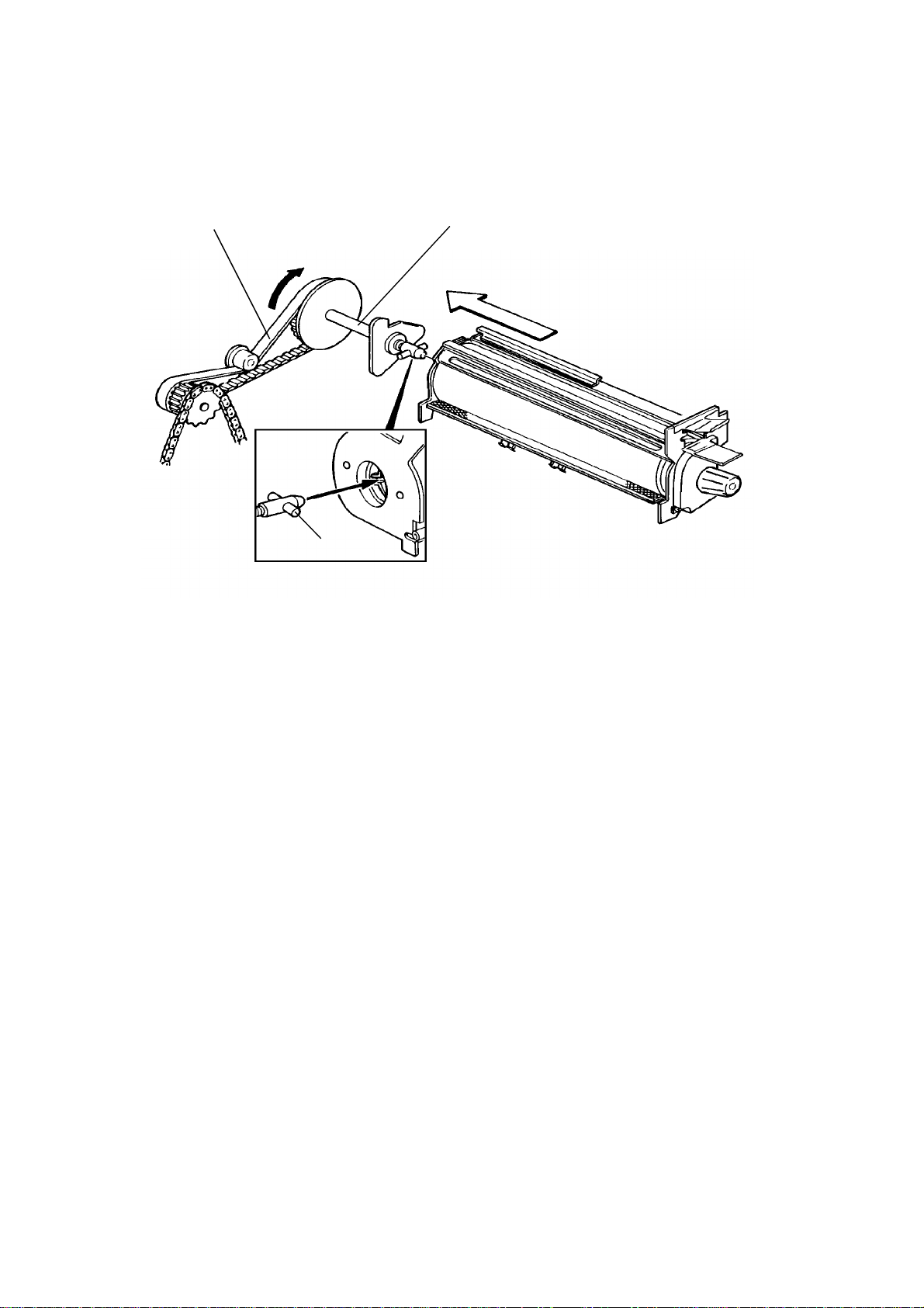
Page 54

1 February 1994 IMAGE PROCESSING
There are other filters for this process. Normally, the filter used is the filter
above but these filters can be selected by SP4-407-2 depending on the
original. The type of filter for each SP4-407-2 setting are as follows.
0:
1 2 2 2 1
1 4 4 4 1
2 4 8 4 2
1 4 4 4 1
1 2 2 2 1
1:
1 2 2 2 1
2 4 4 4 2
2 4 4 4 2
2 4 4 4 2
1 2 2 2 1
2:
1 1 1 1 1
1 1 1 1 1
1 1 1 1 1
1 1 1 1 1
1 1 1 1 1
(High contrast)
(1/64)
Detailed
Descriptions
(Standard)
(1/64)
(Low contrast)
(1/25)
SP4-407-2 is normally set at 1. Set it at 2 to improve the reproduction of low
contrast originals.
2-33
Page 55

IMAGE PROCESSING 1 February 1994
4.4.6 Flare Prevention (GA3)
When the CCD scans across the edge of a black solid image, the reflected
light from both the white and black areas go to CCD elements. This will cause
the edge of the image on the copy to be blurred when 16 level grayscale
processing is used. To prevent this, there are two methods. One is optical,
the other is electrical.
The optical one is simply to place a lamp grid above the lamps to minimize
the width of exposure light. The electrical one is to use smoothing filters.
2-34
Page 56

1 February 1994 IMAGE PROCESSING
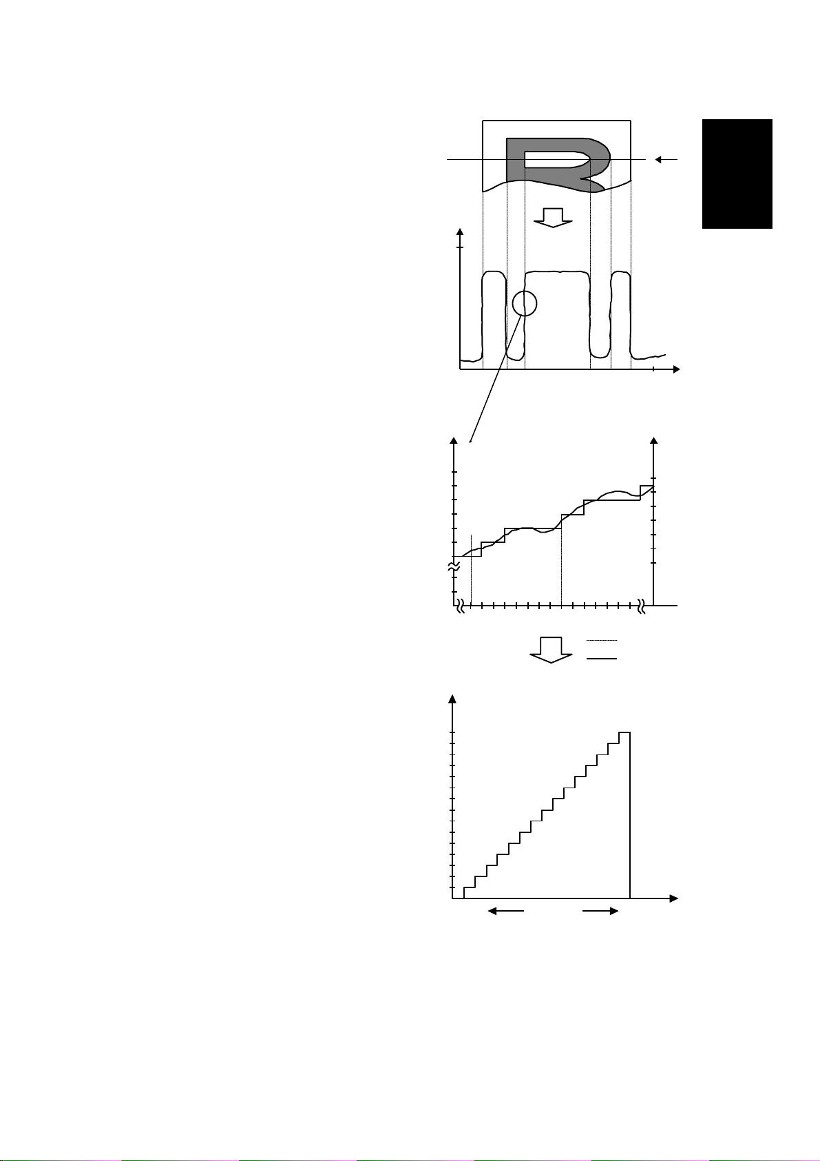
4.4.7 Modulation Transfer Function Correction (GA3)
Black
Real
Image
A
White
Black
CCD
Output
B
White
B
x 100 = MTF (%)
A
When a letter mode or letter/photo mode image is converted to an electrical
signal (for example by a CCD), the signal deteriorates (contrast becomes
less) as the width and spacing of the black and white areas becomes
narrower. The ratio of the difference between the black and white levels of
the signal and the difference between the black and white levels of the
original is called the modulation transfer function or MTF. The MTF is usually
expressed as a percentage.
If the MTF is too low, some parts of the image may be lost. To prevent this,
the image data is enhanced by applying an MTF correction.
Detailed
Descriptions
(a) Section of document (b) Enlarged view of dot
0 0 0 0
0 42 11 0
105
0 42 0
0 11 11 0
0 0 0 0
(c) Image data after
A/D conversion
(d) Copy without MTF
correction
(Threshold level; 127)
2-35
Page 57

IMAGE PROCESSING 1 February 1994
Consider a small black point on a document as shown in the previous
illustration. The 8-bit image data (range 0 to 255) for this section of the
original is shown in (c). If the threshold level is 127, then all the pixels in this
area will become white and the dot will not be reproduced (d).
Such image loss is prevented by providing MTF correction as follows:
-1
-3 -2-2
-1 -3 -3 -1
-2
35
-3
-1
-2
1/11
The value of the pixel is multiplied by 35. Then the new value of the pixel is
reduced by 3 times the value of the pixels to the left, right, above and below,
the values of the pixels two steps to the left, right, above and below, the
values of the pixels to the opposite angles. Then the new value of the pixel is
divided by 11. If the new number is greater than 256, it is reduced to 256.
The MFT algorithm is as follows.
C = {A x (24 x N + 11) + B x N} / 11
A = Value of the object pixel
B = Value of the calculated surrounding the object pixel
N = The strength of the filter
C = Calculated value
0 0 0
0 93 0
0
0
255
0 89
0 0 0.5
0 0 0
(e) Image data after
MTF correction
0
0
0
(f) Copy after MTF correction
After MTF correction is applied the image data of our example becomes as
shown in (e) above. The copy after correction (f) has the dot that was on the
original.
2-36
Page 58

1 February 1994 IMAGE PROCESSING
The MTF algorithm and filter differ by magnification and original type (letter
and letter/photo mode) and they are selected by the CPU. The algorithms
and filters are as follows.
• Letter Mode
Magnification Type of filter Strength of filter
25 ∼ 54%
55 ∼ 79%
80 ∼ 179%
180 ∼ 379%
380 ∼ 800%
• Letter/Photo Mode
A 1/2
A 1
B 1
C 1/2
C 1/4
Magnification Type of filter Strength of filter
25 ∼ 800%
A 1/8
Type of filter
A B C
-1
-4
-3 -3
24
-1-1
-2 -3 -2
-3 -335 -1-1
Detailed
Descriptions
-4
-2 0 -2
-3 -335 -1-1
-4
1/8
-2 -3 -2
-1
-2 0 -2
1/11 1/11
C = {Ax(24xN+11)+BxN}/11C = {Ax(24xN+11)+BxN}/11C = {Ax(16xN+8)+BxN}/8
-4
The strength of the filter can be changed using SP4-407-1 and SP4-407-3.
Normally the value of the SP modes is set at "1", the value of the filter
strength is set according to the above table. If set at "0", each filter strength
value of the above table changes to 1/2 of what it was. If set at "2", the
strength filter value is doubled.
2-37
Page 59

IMAGE PROCESSING 1 February 1994
4.4.8 Main Scan Magnification (GA4)
80% Reduction
Scanned Data
Points
Calculated Data
Points
Reduced Image
Data Points
1 2 3 4 5 6 7 8 9 10
1" 2" 3" 4" 5" 6" 7" 8"
140% Enlargement
Scanned Data
Points
Calculated Data
Points
Enlarged Image
Data Points
1 2 3 4 5 6 7 8 9 10
1"
2" 3" 4" 5" 6" 7" 8" 9" 10" 11" 12" 13" 14"
Reduction and enlargement in the sub scan direction is done by changing the
scanner speed. However, reduction and enlargement in the main scan
direction is handled by the IPU.
Scanning and laser writing are done at a fixed pitch (the CCD elements
cannot be squeezed or expanded). So, to reduce or enlarge an image, GA4
calculates imaginary points that would correspond to a physical enlargement
or reduction of the image. It then calculates the correct image density for
each of the imaginary points based on the image data of the nearest four true
points. The calculated image data then becomes the new (reduced or
enlarged) image data.
NOTE: The actual calculations for main scan magnification uses a process
known as the polynomial convolution method. This mathematical
process is beyond the scope of a service manual and will not be
covered here.
2-38
Page 60

1 February 1994 IMAGE PROCESSING
4.4.9 Gamma Correction (GA5)
HH
CCD
ID
L
L H
Original ID Original ID
CCD
ID
L
L H
This corrects the response of the CCD to the various shades in the gray
scale from black to white. For digital processing techniques to be most
effective, the relationship between original ID and CCD output voltage should
be constant, as shown in the diagram on the left. However, in reality, the
response is more like that shown in the diagram on the right. Gamma
correction corrects this deviation in CCD response.
Detailed
Descriptions
2-39
Page 61

IMAGE PROCESSING 1 February 1994
4.4.10 Grayscale to Black and White Conversion (GA5)
After gamma correction, the image data goes to the functions for 16 level
grayscale. Prior to this each pixel is represented by 8 bits, yielding a 256
level grayscale. The laser uses 4 bits, yielding a 16 level grayscale per pixel.
The 16 level grayscale processing steps convert 8-bit image data to 4-bit
image data suitable for printing. The binary processing steps convert the 8-bit
image data to single-bit image data.
-- 16 Level Grayscale Processing --
Gamma (γ) Correction
Photo mode Letter/Photo mode
8 8
Letter mode
Dithering
8
Error Diffusion
6
Pulse Width
Modulation
4 4
To: Main Board
There are three 16 level grayscale processing methods, depending on the
document mode, as shown in the above illustration.
• Letter Mode
After γ correction, the video data is transformed from an 8 bit data signal
to a 4 bit data signal by the pulse width modulation function.
• Photo Mode
After γ correction, the video data is transformed from an 8 bit data signal
to a 4 bit data signal in accordance with the dither matrix in the ROM (IC
123) on the IPU board.
• Letter/Photo Mode
After γ correction, the video data goes to the error diffusion function where
it reduces the difference in contrast between light and dark areas of the
photo image. The corrected data then goes to the pulse width modulation
function where it is converted to a 4 bit video signal.
2-40
Page 62

1 February 1994 IMAGE PROCESSING
- Binary Processing -
Letter, Photo, Letter/Photo mode
Magnification
6
Binary Processing
1
Main Board
Binary processing, which is used for character or line originals, is simpler
than dithering. Binary processing is performed using the first 6 bits of the 8 bit
data from the magnification function. In binary processing all image data
pixels are compared to a single threshold level. A pixel is set to black if its
value is above the threshold level or it is set to white if it is equal to or below
the threshold level.
The binary processing threshold level for each manually selectable ID level is
shown in the following table.
ID Level 1 2 3 4 5 6 7
Threshold Level 16 24 28 32 40 44 48
Darker Lighter
Detailed
Descriptions
2-41
Page 63

IMAGE PROCESSING 1 February 1994
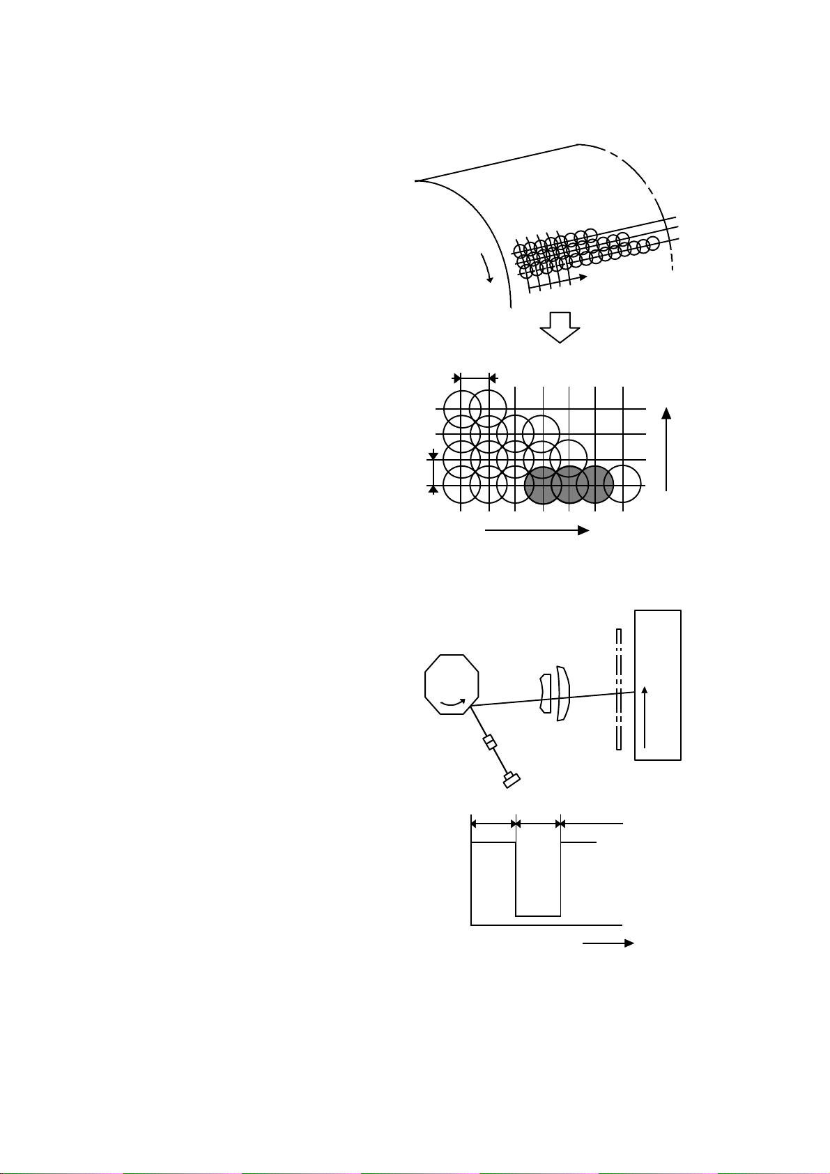
4.4.11 Marker Area Detection (GA6)
Density
Black
63
Threshold
Level
40
14
White
0
Main Scanning
More than 1 mm
(Marker)
More than 1 mm
(Marker)
The marker area detection function determines what parts of the image have
been designated for special processing. The area is designated on the
original using a marker.
Marker area detection is based on the fact that the image density of the
marker ink is between the "black" of the original image and the "white" of the
background areas. As shown in the above illustration, the IPU assumes that
the image element is made by a marker if it has a value above 14 but less
than the threshold level and is wider than 1 millimeter.
When the marker area designation function is used, letter mode is
automatically selected. The default threshold level is 40 (manual ID level 5),
but it can be changed to any other manual ID level using SP4-406.
SP4-406: Marker Density
Adjustable range = 0 to 3 Standard = 0
2-42
Page 64

1 February 1994 IMAGE PROCESSING
4.4.12 Background Numbering (GA6)
Copies have a number appear in the background of the copy. This function
can help the customer keep track of confidential documents.
The patterns for background numbering are stored in a ROM (IC126) on the
IPU. When the background numbering function is selected, the patterns are
sent from the ROM. Then the data will be sent to the laser section.
Image density for the background numbering can be changed using SP4-405.
SP4-405: Background Numbering Density
Adjustable range = 0 or 1 Standard = 1
Detailed
Descriptions
2-43
Page 65

LASER EXPOSURE 1 February 1994
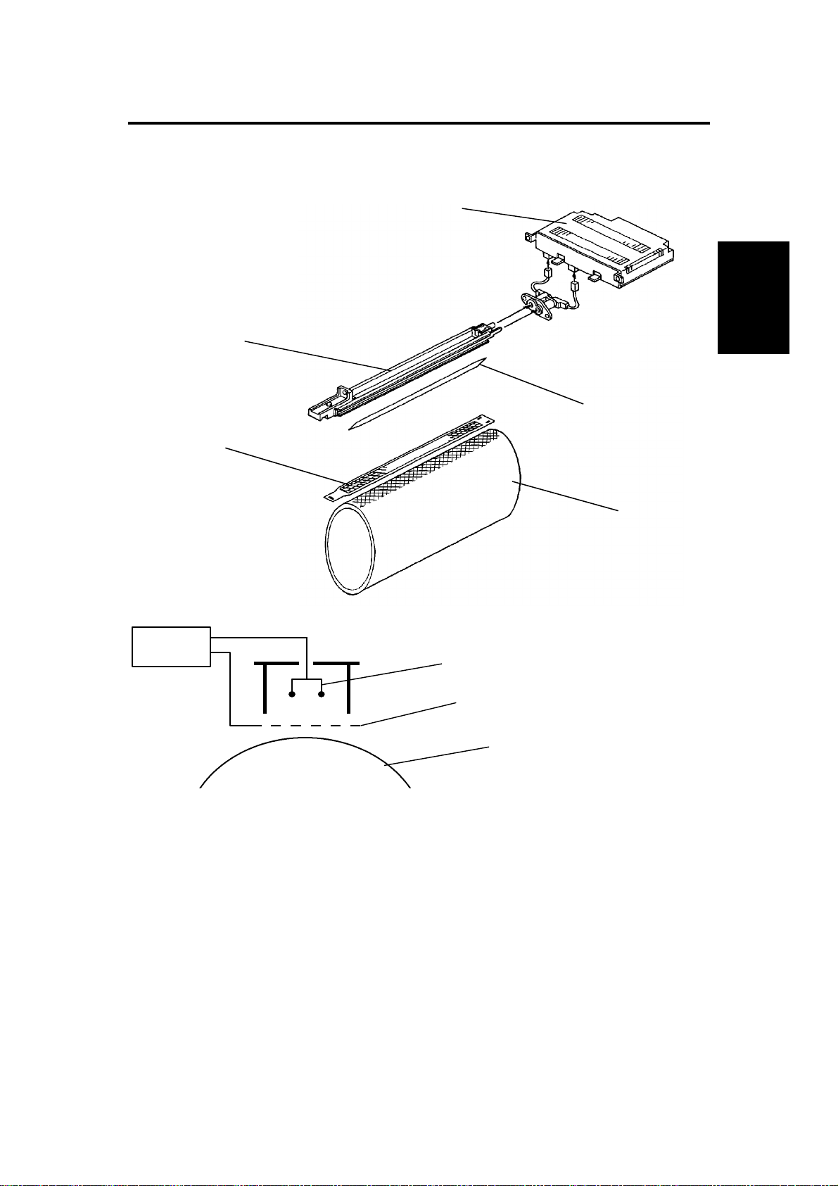
5. LASER EXPOSURE
5.1 OVERVIEW
[B]
[A]
This machine uses a laser diode to produce electrostatic images on an OPC
(organic photoconductor) drum [A]. This gives high picture quality and
enables high-speed writing. The laser diode unit [B] converts image data from
the main PCB into laser pulses through the PWM board, and the optical
components direct these pulses to the OPC drum.
Exposure of the drum by the laser beam creates the latent image. The laser
beam makes the main scan while drum rotation controls the sub scan.
The drum is charged to about --850 volts. The charge on the areas hit by the
laser beam drops to about --100 volts.
2-44
Page 66

1 February 1994 LASER EXPOSURE
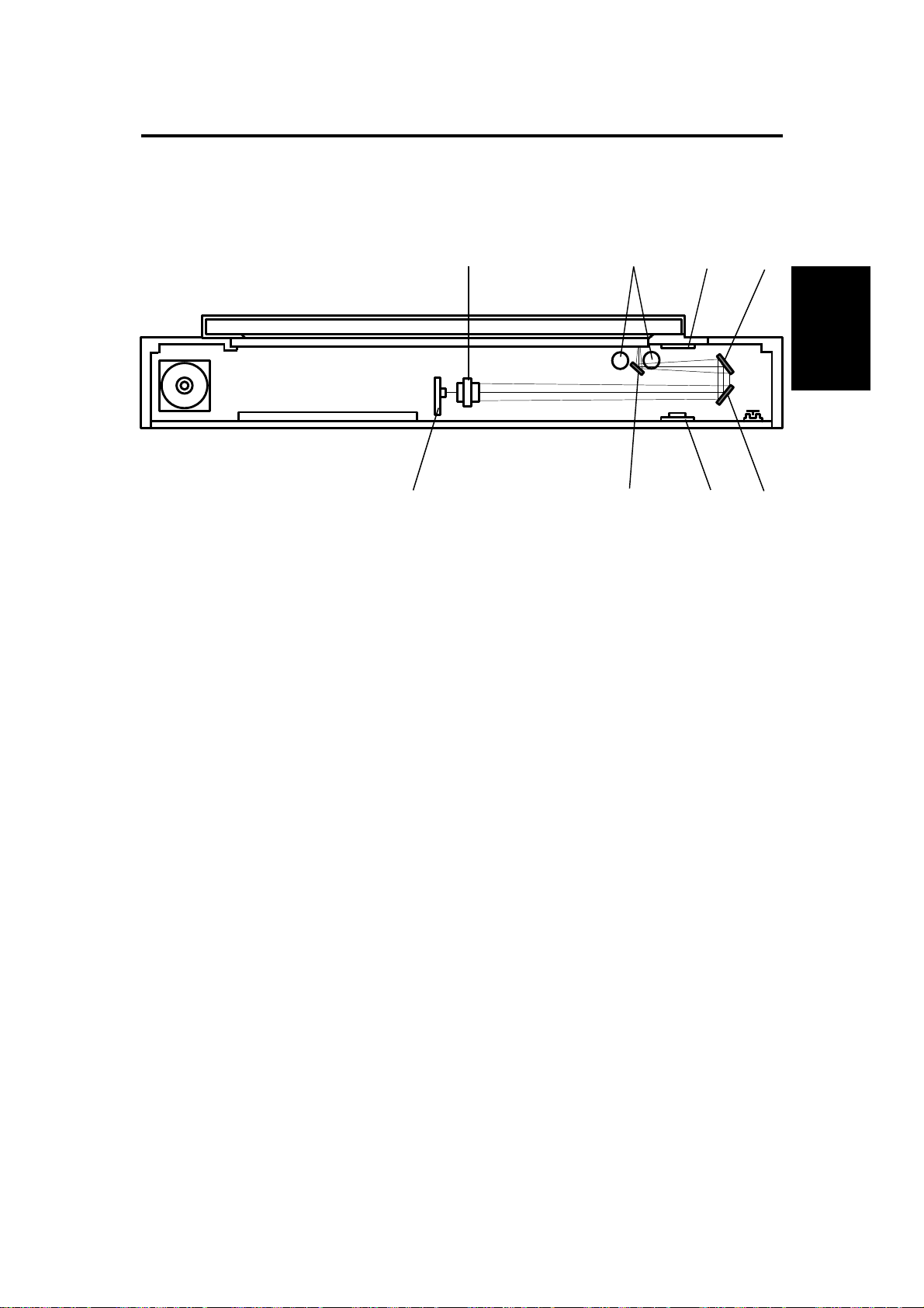
5.2 OPTICAL PATH
[B]
[D]
[E]
[C]
Detailed
Descriptions
[A]
[J]
[F]
[I]
[G]
[H]
The output path from the laser diode to the OPC drum is shown above.
The LD unit [A] outputs the laser beam to the polygon mirror [B] through the
cylindrical lens [C].
The polygon mirror reflects a full main scan line with a single surface of the
mirror. The laser beam goes through the 1st fΘ lens [D] and, 2nd fΘ lens [E].
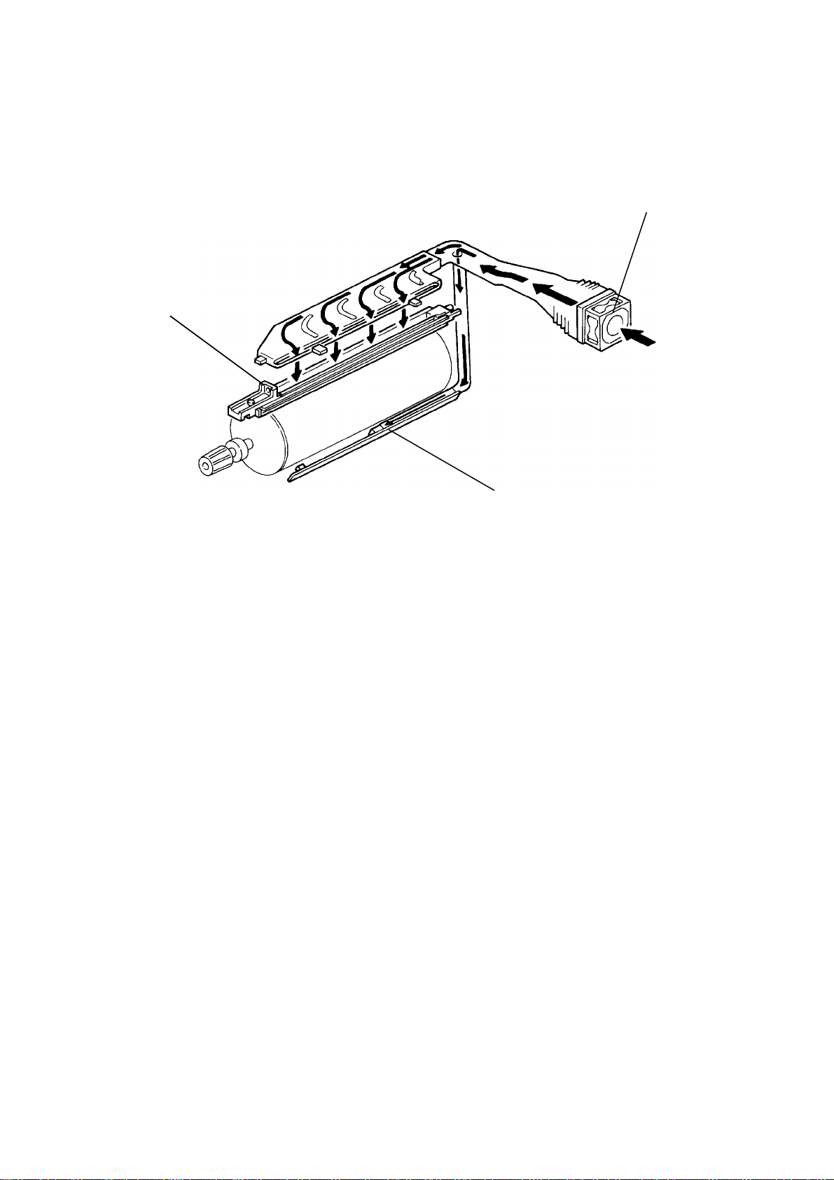
The drum mirror [F] reflects the laser beam to the drum [G] through the toner
shield glass [H].
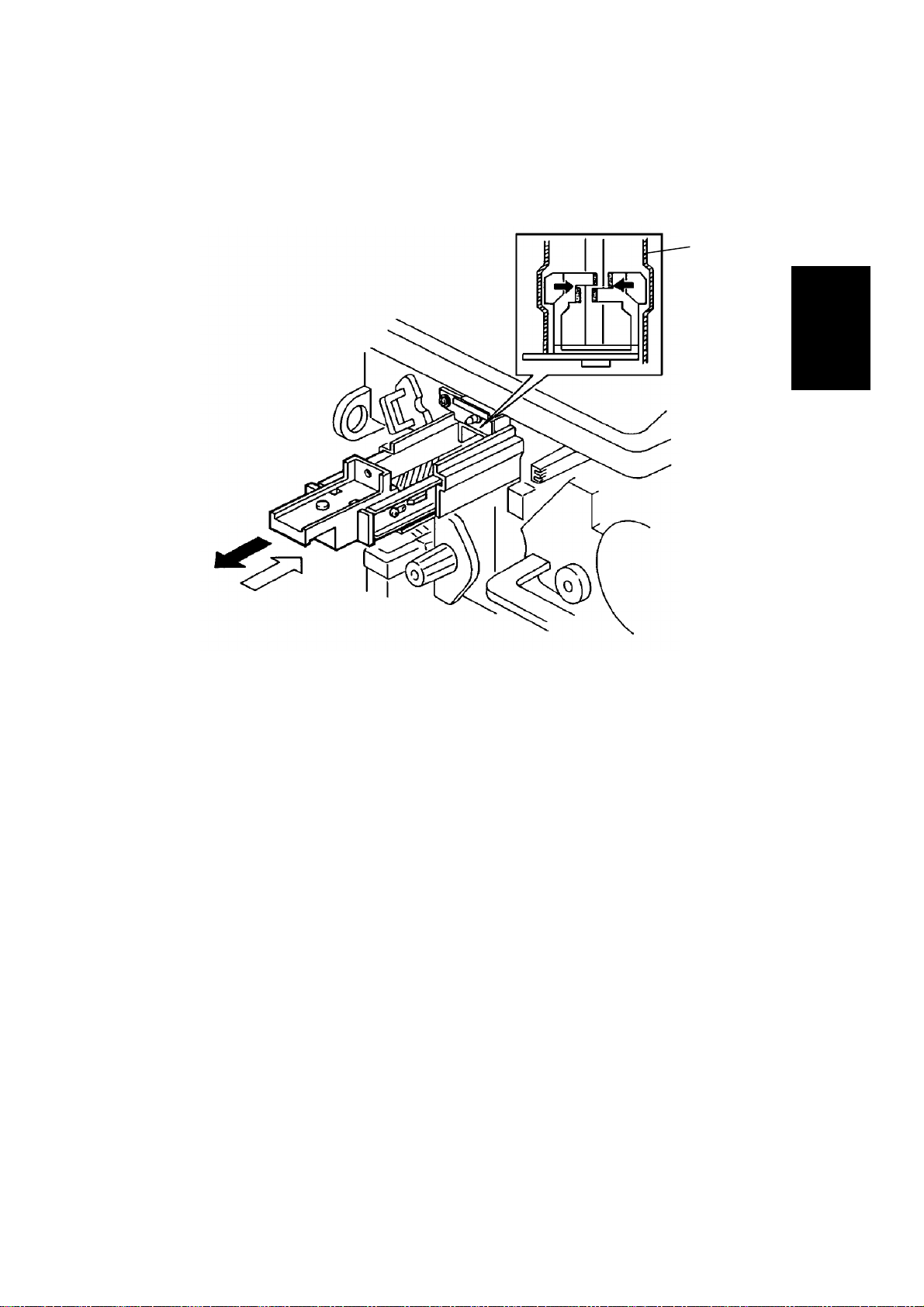
To determine the main scan starting position, the laser beam is reflected from
the the synchronizing mirror [I] to the laser synchronizing detector [J].
The other end of this cable connects to the synchronization detection circuit
on the main board.
2-45
Page 67

LASER EXPOSURE 1 February 1994
5.2.1 Laser Diode Unit
[B]
Laser beam
(to cylindrical
lens)
[A]
[C]
[D]
Laser beam cross
section after
collimating lens
Laser beam cross
section after
aperture
The laser diode unit consists of the laser diode [A], the collimating lens [B],
aperture [C], and the LD driver PCB [D].
The LD driver PCB excites the laser diode, causing it to radiate coherent light
at 780 nm with about 15 mW power.
The collimating lens forms the radiating beams into a parallel beam.
After the collimating lens, the aperture alters the beam, giving it a smaller
cross-section, as shown above.
2-46
Page 68

1 February 1994 LASER EXPOSURE
[C]
[A]
[B]
5.2.2 Cylindrical Lens
The laser beam is focused by the cylindrical lens [A], and sent to the polygon
mirror.
5.2.3 Polygon Mirror
The polygon mirror assembly consists of the polygon mirror motor [B] and the
polygon mirror itself [C].
As the mirror rotates, it reflects the laser beam across the OPC drum, via the
fΘ lens and the drum mirror. One main scan line is made by the beam
reflected from one face of the polygon mirror.
Detailed
Descriptions
The mirror is precisely ground to enable high reflectivity and to prevent pixel
(picture element) misalignment on the drum in both the main scan and sub
scan directions.
2-47
Page 69

LASER EXPOSURE 1 February 1994
5.2.4 F-Theta Lenses
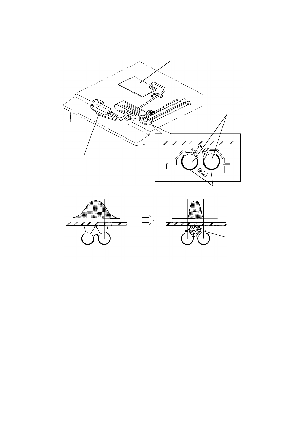
Wide Spaced
Narrow Spaced
[A]
Evenly
spaced
pixels
The angles between pixels are equal. However, if the beam were to go
directly to the drum as shown in the upper illustration, the spacing between
pixels would differ according to the angle of the beam. The pixels near the
end of the drum would be further appart than those near the middle of the
drum. The pixels would also be slightly thicker toward the ends of the drum
than in the middle.
The fΘ lenses [A] correct for this by deflecting the beam slightly inward to
insure uniform picture element spacing and diameter. The fΘ lenses also
correct for irregularities in the polygon mirror face, focusing irregular beams
onto the correct part of the drum.
2-48
Page 70

1 February 1994 LASER EXPOSURE
[A]
[D]
Detailed
Descriptions
[C]
[B]
5.2.5 Drum Mirror
The drum mirror [A] reflects the corrected laser beam to the drum [B].
5.2.6 Laser Synchronizing Mirror and Detector
At the start of each scan line, the synchronizing mirror [C] reflects the laser
beam to the laser synchronizing detector [D] as shown above. Activation of
this detector signals the start of main scan writing by the laser beam.
2-49
Page 71

LASER EXPOSURE 1 February 1994
5.3 LASER EXPOSURE CONTROL
Main Board
IPU
DATA 1, 2
DT12
15
~
DT22
25
~
IC128
Gate
Array
D4 7
~
PWM
Board
LD Unit
IC131
IC132
Line
Buffer
1
Odd
4-bit
Even
4-bit
Odd
4-bit
Even
4-bit
IC129
IC130
Line
Buffer
2
The IPU sends a total of 10 bits of video data to the main PCB (DATA1, 2,
DT12 ∼ 15 and DT22 ∼ 25).
The gate array combines the input data signals into a 8 bit video data signal
(4-bit odd data and 4-bit even data) and then stores the combined data in one
of two line buffers (line buffer 1 or line buffer 2). The two line buffers are used
alternately and hold one scan line of video data each.
When it is time for the data to be written to the drum, the data in the line
buffer returns to the gate array. The gate array combines the read data
signals into 4-bit video data to be written to the drum. The gate array then
sends it to the PWM board.
2-50
Page 72

1 February 1994 LASER EXPOSURE
5.4 PULSE WIDTH MODULATION (PWM)
Black
(F)
(0)
White
Video
data
BlackWhite Gray
Letter mode Letter/Photo mode
0 0 0
1 4 4
2 6 6
3 8 8
4 10 10
5 12 14
6 14 18
7 16 22
8 18 26
9 20 30
A 22 34
B 26 38
C 30 42
D 38 46
E 46 50
F 54 54
Pulse width (ns)
Detailed
Descriptions
To make the latent image, the laser beam exposes the image area of the
drum surface. The longer the laser beam exposes the drum, the darker the
image is developed. The laser on-time for one pulse is controlled using a
pulse width modulation (PWM) circuit.
The video data is sent from the main board to the PWM board through the 4
bit data. In accordance with this 4 bit data, the pulse width for each pixel can
be changed over 16 levels as shown in the table.
2-51
Page 73

LASER EXPOSURE 1 February 1994
5.5 AUTO POWER CONTROL (APC)
IPU
VIDEO
Main Board
15
Main
CPU
+5V
TP107
VR101
IC128
IC125
IC141
IC140
Seq.
CPU
GA
VD
D/A
GA
PWM
A/D
5V
4
Analog
8
Analog
PWM
IC104
Pulse
Generator
VIDEO
LEVEL
LDB
APC
IC2
VR1
LD Unit
LD1
IC3
LD
Driver
Q1
-12V
IC2
VR2
IC2
Even if a constant electric current is applied to the laser diode, the intensity of
the output light changes with the temperature. The intensity of the output
decreases as the temperature increases. In order to keep the output level
constant, the output light intensity is monitored through a photodiode and the
current to the laser diode is increased or decreased as necessary. The main
PCB checks the output of the laser diode at the beginning of the first copy
cycle and after every 10 copies. The procedure for checking and controlling
the laser power is as follows:
• The main PCB sends an all black data signal to the LD unit (VIDEO),
which causes the laser diode to turn on.
• The sequence CPU on the main PCB monitors the feedback signal (APC)
from the photodiode in the LD unit.
• If the APC is less than 3 volts, the sequence CPU increases the voltage
of the power control signal (LEVEL) through the D/A converter, and the
other power control signal (LDB) through the gate array PWM. If the APC
is more than 3 volts, the CPU decreases LDB.
The sequence CPU does not control the laser power during printing. This is
because the laser output is not constant during printing, so power control
would be inaccurate. The reference voltage is adjusted by VR101 in the
factory, so that the proper laser power is applied to the drum surface when
APC is 3.0 V.
2-52
Page 74

1 February 1994 LASER EXPOSURE
5.6 LASER SYNCHRONIZING DETECTOR
[B]
[A]
Main Board
Detailed
Descriptions
10
VIDEO
IC128
Gate
Array
VD
4
To PMW Board
VIDEO
To IPU
IPU
VIDEO
CN161-2
Detected Signal
CN161-1
Q202
+5V
TP103
10
IC128
Gate
Array
VD
VIDEO
IC138
Gate
Array
IO
PMSYNC
At the start of each scan line, the synchronizing mirror [A] reflect the laser
beam to the main PCB through the laser synchronizing detector cable [B].
Activation of this detector signals the start of main scan writing by the laser
beam.
The laser beam is received by the gate array VD (IC128) on the main PCB.
After receiving the beam, the gate array generates a signal (PMSYNC) and
then sends it to the gate array IO (IC138). IC138 controls the timing for the
video data printing, in accordance with the signal. The (PMSYNC) is also
used to control the timing of IPU operation.
2-53
Page 75

LASER EXPOSURE 1 February 1994
5.7 LD SWITCH
DC Power
Supply
Front Door
Safety SW
5V
CN50 CN104
-8
[A]
PWM
LDSW Q101
-1
-12V
[B]
CN102-6
CN101-6
LD5V
LD
Dr.
LD Unit
LD1
To ensure that the laser beam does not inadvertently expose the drum at
servicing, there are two LD switches located at the front door. These two
switches [A] are installed in series on the LDSW line coming from the dc
power supply board.
When a front door is opened, the switches cut the power to CN104-1 (LDSW)
of the PWM board. Then, dc 5 volts (LD+5V) for LD power [B] cannot be
supplied to the LD drive board.
2-54
Page 76

1 February 1994 DEVELOPMENT
6. DEVELOPMENT
6.1 OVERVIEW
[E]
[C]
This copier uses a double roller development (DRD) system. This system
differs from single roller development system in that (1) it develops the image
in a narrower area, (2) it develops the image twice, and (3) the relative speed
of each development roller against the drum is reduced. Also, finer toner and
developer (smaller particle size) are used. Both DRD system and new
supplies improve the image, especially of thin horizontal lines, the trailing
edges of the half-tone areas, and black cross points.
When the development clutch is turned on while the main motor is rotating,
the agitators [A], paddle roller [B] and two development rollers [C] start
turning. The paddle roller picks up developer in its paddles and transports it
to the lower development roller. Internal permanent magnets in the
development rollers attract the developer to the development roller sleeve.
The turning sleeve of the lower development roller carries the developer to
the upper development roller. The upper development roller carries the
developer past the doctor blade [D]. The doctor blade trims the developer to
the desired thickness and creates backspill to the cross mixing mechanism.
[D]
[A]
[B]
Detailed
Descriptions
The development rollers continues to turn, carrying the developer to the OPC
drum [E]. When the developer brush contacts the drum surface, the areas of
the drum surface that have a low negative charge attract and hold the
negatively charged toner. In this way, the latent image is developed.
The development rollers are given a strong negative bias in order to create
an electrical potential between the development rollers and the areas of the
drum where the laser has dissipated the negative charge.
After turning another 100 degrees, the developer is released to the
development unit.
2-55
Page 77

DEVELOPMENT 1 February 1994
6.2 DRIVE MECHANISM
[F]
[G]
[B]
[E]
[D]
[C]
[A]
The development clutch gear [A] turns when the main motor is on. The
development clutch [B] controls transmission of this rotation to the
development drive gear [C].
The development drive gear turns both the upper and the lower development
rollers via their drive gears [D].
This rotation is also transmitted to the front side through the mixing auger [E]
and then turns the paddle rollers and the agitators via gears [F].
The paddle roller shaft has a knob [G] on its front end to facilitate gear
engagement and to turn the rollers for developer exchange. The paddle roller
knob has a one-way clutch inside. The one-way clutch prevents the
development roller from turning in the opposite direction, which would cause
the developer brush to damage the upper brush seal.
2-56
Page 78

1 February 1994 DEVELOPMENT
6.3 CROSS-MIXING
[C]
[F]
Detailed
Descriptions
[D]
[A]
[B]
[E]
[A]
[D]
This copier uses a standard cross-mixing mechanism to keep the toner and
developer evenly mixed. It also helps agitate the developer to prevent
clumping and help create the triboelectric charge.
The developer on the turning development rollers [A] is split into two parts by
the doctor blade [B]. The part that stays on the development roller forms the
magnetic brush and develops the latent image on the drum. The part that is
trimmed off by the doctor blade goes to the backspill plate [C].
As the developer slides down the backspill plate to the paddle roller [D], the
mixing vanes [E] move it slightly toward the rear of the unit. Part of the
developer falls into the auger inlet and is transported to the front of the unit by
the mixing auger [F].
2-57
Page 79

DEVELOPMENT 1 February 1994
6.4 DEVELOPMENT PROCESS
--100 volts on the
image areas
(exposed by
laser).
--850 volts on
the nonimage
areas
--600 V
--600 V
[A]
Several forces interact in the development process to produce a visible
image on the OPC drum. These forces are the charge pattern of the latent
image, the development bias, the magnetic field of the development roller,
the positive triboelectric charge of the carrier, and the negative triboelectric
charge of the toner.
One of the most important of these forces is the charge pattern of the latent
image on the drum. To make the latent image, the laser exposes an area of
the drum surface corresponding to the dark parts of the original image. The
laser reduces the charge on the drum surface in these areas from about
--850 volts to about --100 volts. The latent image is thus formed as a pattern
of --100 volts and --850 volts.
The C/G/B/BR power pack applies a bias of --600 volts to the development
rollers. Also, a magnetic field between the drum and the development sleeve
is created by strong magnets [A], which are placed inside the development
rollers close to the sleeve.
The developer consists of carrier and toner. The carrier particles are made of
ferrite with a surface coating and are about 70 µm in diameter. The toner
particles are made of resin and carbon black and are approximately 9 µm in
diameter. The toner is negatively charged and the carrier is positively
charged by rubbing action within the development unit.
2-58
Page 80

1 February 1994 DEVELOPMENT
In the development area, the following forces act on the toner particles:
FC: The attractive force between
toner (--) and carrier (+)
FD: The repelling force between
toner (--) and the drum
charge (--)
FB: The repelling force between the
toner (--) and the development
roller bias (--)
The exposed areas of the drum
have the relationship of:
FB > FC + FD (Fig.1)
Which causes toner to be repelled
from the carrier to the drum. (FD is
very small.)
The non-exposed areas of the drum
have the relationship of:
FB < FC + FD (Fig. 2)
Here FD is very large and repels
toner from the non image areas.
You might expect that the positively
charged carrier would be attracted
to the negatively charged non-image
areas of the drum. However, this
does not happen. In the development area, the following forces act
on the carrier particles:
FMC: The attractive force of the
magnet on the carrier
FBC: The attractive force between
the carrier and development bias
FDC: The attractive force between the
carrier (+) and the non-exposed
areas of the drum (--)
Since FDC < FMC + FBC (Fig. 3), the
carrier remains on the development
roller’s sleeve.
DRUM
-100V
Fig. 1
DRUM
-850V
Fig. 2
DRUM
-850V
Fig. 3
F
F
B
B
Carrier
F
DC
Toner
F
Toner
Fc
F
D
BC
F
MC
DEV.
ROLLER
-600V
Carrier
Fc
F
D
Detailed
BIAS
DEV.
ROLLER
-600V
Carrier
BIAS
DEV.
ROLLER
-600V
MAGNET
BIAS
Descriptions
2-59
Page 81

DEVELOPMENT 1 February 1994
6.5 BIAS CONTROL
Main Board C/G/B/BR Power Pack
B1-Trigger
B2-Trigger
B1-PWM
B2-PWM
CN156
-A8
-A9
-A3
-A4
CN511
-2
-1
-7
-6
5
5
5
5
Bias (1)
Development
GND-Vcc
-A1
+24V (V )
AA
CN510
GND
0
-9
24
-1
0
-3
Bias (2)
The development biases are controlled by the PWM signals (CN156-A3 and
-A4).
Status
1 Stand by: 0V
2 Ready: +250 V
3
Charged area start: +250 V → --430 V → --600 V
4 Image area: --600 V
5 ID sensor area: --430 V
6
Charged area finish: --600 V → --430 V → +250 V
In the stand-by mode, the development bias is 0V. When the development
roller starts rotating, the development bias is changed to +250 V. When the
drum charging process begins, the development bias is changed to --430 V. If
the development bias were to remain at +250 V during charging, the positive
carrier would be attracted to the negatively charged drum, and the negative
toner would stay on the development roller. The bias is set to --430 V during
the initial charging period to prevent this toner-carrier break down. The toner
must be kept on the development roller until the image area of the drum
reaches the development roller.
The development bias is then dropped to --600 V and remains at this voltage
through out the image development process. If the development bias were
changed to --600 V before the image development begins, toner would be
attracted to the drum before the image area. This would cause toner to be
wasted and toner scattering.
After the image is developed, this three-step voltage change sequence is
reversed.
These development bias changes are controlled by the PWM circuit as
shown on the table.
2-60
Page 82

1 February 1994 DEVELOPMENT
6.6 TONER DENSITY DETECTION
[B]
[C]
Detailed
Descriptions
[A]
[A]
A: Developed sensor pattern
B: Low toner
C: Enough toner
The main board checks toner density by directly sensing the image density at
the end of the first copy cycle after the main switch is turned on, and at every
10th copy after that. (The machine can be set to check toner density every 5
cycles using SP2-209.)
On check cycles, the CPU sends the laser on signal to make the pattern
image (20 x 20 mm) on the drum surface. After the sensor pattern is
developed, its reflectivity is checked by the image density sensor. The CPU
notes the strength of reflectivity. If the reflected light is too strong, indicating
the toner density condition is too low, it adds toner to the development unit.
The toner is not added all at once. The CPU energizes the toner supply
solenoid and adds a selected amount of toner over the next 10 cycles.
2-61
Page 83

DEVELOPMENT 1 February 1994
6.7 TONER DENSITY CONTROL
ID Sensor Board
ID Sensor
V
SG
Threshold
Level
.
SG
n V
CN-3
CN-1
CN-A
CN-C
CN-B
Vcc [5]
VCA [12]
CN151
-A3
-A1
-A2
ID Sensor
[1.2--4.7]
Main Board
GND Vcc [0]
ID Sensor LED
Toner
Supply
Sol.
[▼5 ]
Toner is supplied.
V
SP
No toner is supplied.
0
The CPU receives two voltage values (Vsg and Vsp) directly from the image
density (ID) sensor through CN151-A3. Vsg is the value for the bare drum
and Vsp is the value for the sensor pattern. The CPU compares these two
values to determine if more toner should be added.
NOTE: Vsg is 4.0 volts when adjusted properly.
-- Toner Supply Condition --
Vsp ≥ n . Vsg ⇒ Low image density (toner added)
Vsp < n . Vsg ⇒ High image density (no toner added)
("n" is the toner add coefficient)
When the density of the developed pattern becomes low, the light reflected to
the phototransistor from the sensor pattern increases. This causes Vsp to
increase. When Vsp becomes greater than the toner add level (n . Vsg) the
CPU activates the toner supply solenoid to add a selected amount of toner
over the next 10 copy cycles.
2-62
Page 84

1 February 1994 DEVELOPMENT
-- Add Toner Level --
The coefficient "n", which determines the add toner level, is adjustable using
SP2-211.
Never change this SP setting to increase or decrease toner setting. Use
SP2-201-4.
SP2-211: Toner Add
Display N LL L H
Coefficient "n" 1/13 1/9 1/11 1/15
Toner add detected level Standard
0.31 V
Lowest
0.44 V
Low
0.36 V
High
0.27 V
Default: N
-- ID Sensor Bias --
The bias voltage used for the development of the ID sensor pattern is not the
same as for the image development. The ID sensor bias is adjustable using
SP2-201-4.
SP2-201-4: ID Sensor Bias
Display 0 1 2 3 4
ID sensor bias --490 V --460 V --430 V --400 V --370 V
Default: 2
As an example of the function of the ID sensor bias, consider what happens
when SP2-201-4 is set to 0 (ID sensor bias = --490 V). The change in bias
causes the potential between the pattern area of the drum and the
development bias to become stronger. As a result, the pattern is developed
with a higher image density, which causes the toner concentration in the
developer to be reduced.
Detailed
Descriptions
-- ID Sensor Abnormal --
If one of the following conditions is detected three times in succession, the
CPU automatically shifts from the detect supply mode to the fixed supply
mode and displays "Clean ID Sensor" in the message display.
• Vsp higher than 2.5 volts
• Vsg lower than 2.5 volts
2-63
Page 85

DEVELOPMENT 1 February 1994
6.8 TONER SUPPLY
[G][H]
[I]
[F]
[E]
[D]
[C]
[A]
[B]
G: Toner Cartridge
H: Toner Agitator
I: Toner Agitator Gear
6.8.1 Roller Drive Mechanism
The toner supply clutch gear [A] turns when the main motor is on. The toner
supply clutch [B] controls transmission of this rotation to the toner supply
drive gear [C].
When the toner supply solenoid [D] energizes, the toner supply clutch
engages and starts turning the toner supply drive gear. The toner supply
drive gear turns the toner supply roller gear [E]. Toner catches in the grooves
in the toner supply roller [F]. Then, as the grooves turn past the opening, the
toner drops into the development unit.
2-64
Page 86

1 February 1994 DEVELOPMENT
6.8.2 Toner Agitator Drive Mechanism
[A]
[C]
[B]
Detailed
Descriptions
The toner agitator mechanism, which is in the toner cartridge, prevents toner
from blocking.
The toner agitator gear [A] engages with the toner supply roller gear through
an idle gear [B]. Therefore, the toner agitator gear turns when the toner
supply clutch engages.
Rotation passes through the toner cartridge casing to the agitator junction [C].
2-65
Page 87

DEVELOPMENT 1 February 1994
6.9 TONER SUPPLY MODE AND AMOUNT
This copier has four different ways of controlling the amount of toner
supplied. Normally, the detect supply system controls toner supply. However,
other supply systems can also be selected, depending on the type of original,
by SP2-208-1.
SP2-208-1: Toner Supply Mode
Display 0: D 1: F 2: DF 3: A
Mode Detect Fixed Detect + Fixed Auto
Default: 0
6.9.1 Detect Supply Mode
When SP2-208-1 is set to 0, the detect supply mode is selected. If Vsp
becomes greater than n . Vsg, a small amount of toner is added by the toner
supply solenoid on each of the next 10 copy cycles. (The machine can be set
to check ID and add toner in 5 cycle increments by SP2-209.)
SP2-209: I.D.S. Check Interval
Display 0: 10 1: 5
Check interval 10 copies 5 copies
Default: 0
When toner supply amount is increased, 5 cycle increments is better than 10
cycle to keep good toner concentration control in the developer.
Toner supply starts 90 pulses after the exposure lamp turns off. (Toner is
supplied at this time to prevent toner scattering on the copies.) The actual
amount of toner added is determined by controlling the length of time that the
clutch is on. Toner supply amount is adjustable by SP2-208-2.
6.9.2 Fixed Supply Mode
If SP2-208-1 is 1 or ID sensing is abnormal, the CPU selects the fixed supply
mode. In this case, a fixed amount of toner is added every copy cycle.
SP2-208-2: Toner Supply Amount
Display 0: N 1: L 2: H 3: HH
Detect supply 30% 15% 45% 60%
Fixed supply 7% 4% 11% 14%
Default: 0
2-66
Page 88

1 February 1994 DEVELOPMENT
6.9.3 Detect + Fixed Supply Mode
When SP2-208-1 is set to 2, the detect + fix supply mode is selected.
In the condition that Vsp is greater than n . Vsg, the toner supply is controlled
by the detect supply mode.
Even if Vsp becomes lower than n . Vsg, a small amount of toner (2%) is
supplied every copy cycle. If Vsp becomes lower than
1
⁄
n . Vsg, no toner is
2
supplied.
6.9.4 Auto Supply Mode
When SP2-208-1 is set to 3, the auto supply mode is selected. In this mode,
the detect supply mode is also used for the overall toner density control.
In addition, the CPU counts the time the laser is on for every original.
Through this data, the CPU estimates how much toner should be added to
compensate and adds this amount of toner during next copy cycle.
Detailed
Descriptions
For the customer who makes copies from high-coverage originals, this mode
should be selected to minimize the fluctuation of the image density.
2-67
Page 89

DEVELOPMENT 1 February 1994
6.10 TONER END DETECTION
6.10.1 Toner Near End Detection
The toner near end level is reached when Vsp has increased a certain
amount over the level at which toner is added. This level is determined as
follows:
Vsp(toner near end) = n . Vsg(add toner level) + V(increase)
The amount that Vsp must increase before the toner near end condition is
reached depends on the setting of SP2-212.
SP2-212: Toner Near End
Display 0: N
(+0.20 V)
1: L
(+0.25 V)
2: H
(+0.15 V)
Default: 0
The normal setting of SP2-212 is 0. If the toner end setting and add toner
setting are both at the normal setting and the image density sensor is
adjusted properly (Vsg = 4.0 V), then the toner near end level is reached
when Vsp = 0.51 volt ((
1
⁄
x 4.0) + 0.20).
13
If the CPU detects the toner near end level three times in succession, the
Add Toner indicator starts blinking. This is Toner Near End condition.
6.10.2 Toner End
After Toner Near End condition occurs, up to 50 copies can be made (toner
end copy run). If a new toner cartridge is not added within that interval, the
Add Toner indicator stays on. Copying is then inhibited until a new toner
cartridge is added.
The toner end copy run can be set to 20 copies rather than 50 using SP2-213.
SP2-213: Toner End Copy Run
Display 0: 50 1: 20
Default: 0
2-68
Page 90

1 February 1994 DEVELOPMENT
6.10.3 Toner End Run Additional Toner Supply
During the toner end indicator blinking, the toner supply solenoid and the
main motor stay on for an additional period after the copy job is finished.
This adds extra toner in order to recover the image density level. This is
necessary because it is possible for Vsp to exceed the toner near end level
even though there is sufficient toner in the cartridge if originals with large dark
image areas are copied. Once Vsp drops below the toner near end level, the
copier is reset to normal. The time period for the additional toner supply is set
by SP2-210.
SP2-210: Toner Add Time
Adjustable range = 4 to 9 Default = 8
With SP2-210, the toner add time increases as the number (n) entered gets
larger.
The actual time of toner supply solenoid activity can be calculated with the
following formula: 1.4 sec x n (n = 4 to 9)
Detailed
Descriptions
2-69
Page 91

TRANSFER AND SEPARATION 1 February 1994
7. TRANSFER AND SEPARATION
[B]
[D]
[A]
[C]
7.1 IMAGE TRANSFER
The registration rollers [A] feed the copy paper through the transfer entrance
guides to the transfer section. A high positive voltage (+6.0 kilovolts) is
applied to the transfer corona wire [B], and the corona wire generates
positive ions. These positive ions are applied to the copy paper, and the
positive charge attracts the negatively charged toner away from the drum and
onto the paper. In addition, the paper is held against the drum by the
negative countercharge on the drum.
7.2 PAPER SEPARATION
After image transfer, the paper must be separated from the drum. The
separation corona wires [C] generate an ac corona which breaks the
attraction between the paper and the drum. The pick-off pawls [D] aid in
separating light weight paper and paper that has low stiffness.
The separation corona has both ac and dc components. The ac component
is constant (5.3 ± 0.2 kV), but the dc component is not. For the first 10 mm of
the copy, the dc component is --90 µA, but for the rest of the copy the dc
component shifts to --25 µA. This helps the leading edge of the paper to
separate from the drum. (If --90 µA were applied to the entire sheet, image
transfer would be adversely affected.)
2-70
Page 92

1 February 1994 TRANSFER AND SEPARATION
7.3 TRANSFER/SEPARATION CORONA CIRCUIT
T/D/PCC Power Pack
DC Drive Board
T-Trigger
S-Trigger
CN703
-A12
-A11 -5
CN512
-4
Transfer
Main Board
T-PWM
S(AC)-PWM
S(DC)-PWM
GND
CN151
-A10
-A9
-A8
-A7
+24V (V )
CN513
-1
-2
-3
-4
CN512-1
-3
AA
GND
Separation
T/S Corona Unit
The above diagram shows the transfer/separation corona circuit. The dc
power supply board supplies +24 volts (VAA) to CN512-1 of the T/D/Pcc
power pack.
The dc drive board sends the transfer and the separation trigger signals
(active LOW) from CN703-A12 and -A11.
Detailed
Descriptions
CN151-A8, -A9, and -A10 are used for the PWM control for the transfer and
separation corona. Depending upon the duty of PWM applied, the output can
be changed. The duty of the S(DC)-PWM is changed at the first 10 mm of the
copy, so that the paper can be easily separated from the drum.
Output PWM Duty
Transfer
Separation (AC)
Separation (DC-Edge)
Separation (DC)
+350 ± 15 µA
+5.3 ± 0.2 kV
--90 ± 5 µA
--25 ± 5 µA
2-71
50%
50%
37%
80%
Page 93

DRUM CLEANING 1 February 1994
8. DRUM CLEANING
8.1 OVERVIEW
[C]
[B]
[G]
Drum cleaning is accomplished by
the pre-cleaning corona (PCC) [A],
cleaning brush [B], and cleaning
blade [C].
As the toner enters the cleaning
unit, the PCC unit applies an ac corona with a negative bias. The ac
component of the PCC removes any
positive charge remaining on the
drum from the transfer corona. The
negative dc component of the PCC
gives the toner a uniform negative
charge, which makes it easier for
the cleaning brush to remove the
toner.
[A]
[D]
[B]
[F]
[E]
[C]
[A]
2-72
Page 94

Detailed
Descriptions
1 February 1994 DRUM CLEANING
In this model the cleaning brush removes more of the toner than the cleaning
blade. This is because it uses electrical as well as mechanical action to
remove the toner. The cleaning brush has a positive charge, which it receives
from the bias roller [D], and electrically attracts the negatively charged toner.
After picking up the toner, the cleaning brush turns inside the cleaning unit.
Just inside the unit, it brushes against a beater bar [E]. The beater bar
dislodges paper dust and some of the toner.
Next the cleaning brush brushes against the bias roller. The bias roller, which
has a charge of +150 volts, attracts the toner from the cleaning brush. The
bias roller blade [F] scrapes the toner from the bias roller and the toner drops
on the toner collection coil [G]. The cleaning blade removes the remaining
toner.
The toner collection coil transports the used toner to the front of the machine
where it falls into the used toner bottle.
2-73
Page 95

DRUM CLEANING 1 February 1994
8.2 DRIVE MECHANISM
[D]
[C]
[B]
[A]
The main chain [A] drives the cleaning unit when the main motor is on. The
brush gear [B] fits into the cleaning drive sprocket. A pin [C] on the inside of
the sprocket turns the brush gear by pushing on the tab. The brush gear
drives the bias roller gear [D] and the collection coil gear.
2-74
Page 96

Detailed
Descriptions
1 February 1994 DRUM CLEANING
8.3 CLEANING BLADE PRESSURE MECHANISM
[F]
[D]
[C]
[B]
[E]
[A]
[G]
[F]
When the cleaning solenoid [A] turns on, it turns the cleaning solenoid lever
[B] clockwise (rear view). The pressure arm [C] turns clockwise and presses
the cleaning blade lever [D] as shown above. The cleaning blade holder [E]
then rotates and presses the cleaning blade [F] against the drum.
The cleaning blade is mounted by a single swivel screw at its exact center of
mass. With this type of mounting the blade sets parallel and applies even
pressure automatically. Also since pressure is transmitted in the center, a
single pressure spring is used.
The blade scraper [G] contacts the bottom of the cleaning blade. When
pressure is applied to the cleaning blade, the blade presses against the drum
and bends at its outer edge. When pressure is released from the blade, it
snaps back to its original shape. The mylar of the blade scraper then scrapes
off the excess toner and paper dust from the edge of the blade.
The cleaning solenoid is deactivated at the following times:
• when the main switch is off
• after every 100 copies
• when the front doors are opened
• after 20 minutes without copy operation
2-75
Page 97

DRUM CLEANING 1 February 1994
8.4 TONER COLLECTION BOTTLE VIBRATION
[D]
[B]
[C]
[E]
[A]
[G]
[F]
The toner collection bottle [A] is vibrated to prevent toner from building up in
one place and activating the toner overflow sensor too early.
The main drive chain turns the drive sprocket [B]. The drive sprocket has a
gear on the reverse side which turns the cam drive gear [C]. A pin on the cam
drive gear rotates the cam wheel [D]. This wheel has six slots in which the pin
catches; so, the cam wheel turns 1/6 of a revolution for each full turn of the
cam drive gear.
The cam [E] of the cam wheel pushes the cam lever [F] out as it turns. The
pin on the other end of the cam lever pushes the vibration link [G] toward the
front of the copier. This link pushes the toner collection bottle against a spring
installed inside the bottle cover. When the cam wheel completes one turn, the
cam lever is released and the spring pushes the toner collection bottle
quickly toward the rear of the copier. This action keeps the toner level inside
the toner collection bottle.
2-76
Page 98

Detailed
Descriptions
1 February 1994 DRUM CLEANING
8.5 TONER OVERFLOW SENSOR CIRCUIT
+5 (Vcc)
OSC
CN3-3
Toner Overflow Sensor
Freq.
Detection
Rectifier
Tr.
CN36
-2
Main Board
CN155
-B6
5
Toner
Overflow
Sensor
The toner overflow sensor signals the CPU when the toner collection bottle is
full.
A tiny tuning fork is used as the sensing element of the toner overflow
sensor. This tuning fork is a damping element in a multivibrator circuit. As
long as there is nothing in contact with the tuning fork, the vibrating frequency
of the circuit stays low and the transistor stays off.
When toner presses against the tuning fork, the resistance of the
piezoelectric elements that are in contact with the tuning fork changes and
the vibrating frequency increases. The frequency detection circuit passes the
higher frequency signal to the rectifier which activates the switching
transistor. The transistor sends a LOW signal to CN155-B6.
When the CPU detects this LOW signal, the Used Toner Bottle indicator
starts blinking. This is Used Toner Bottle Near Full condition. 2,000 copies
1/2" x 11"/A4 size) after the Near Full condition occurs, the Used Toner
(8
Bottle indicator stays on and copying is then inhibited. To clear this condition,
empty the used toner bottle and set SP7-806 (Used Toner Counter Clear).
2-77
Page 99

DRUM CLEANING 1 February 1994
8.6 PCC, BIAS ROLLER, AND CLEANING SOLENOID
CIRCUITS
DC Drive Board
PCC Trigger
Main Board
Br. Trigger
PCC AC PWM
PCC AC PWM
GND PCC
Clearing Sol.
▼5]
[
▼5]
[
[0]
[
▼24]
CN703-A10
CN156-A5
CN151-A6
CN151-A5
CN151-A4
CN703-A13
24V (VAA)
CN512-6
CN513-5
CN513-6
CN513-7
CN512-1
CN512-3
GND
Cleaning solenoid
SOL
C/G/B/BR P.P.
BR
Bias Roller
T/D/PCC P.P.
PCC
PCC corona
24V (VAA)
8.6.1 PCC and Cleaning Bias
The dc power supply board supplies +24 volts (V
AA) to pins 1 and 3
respectively of both the C/G/B/BR power pack and the T/D/PCC power pack.
To turn on the cleaning bias, the main board drops CN156-A5 to LOW. The
cleaning bias turns on at the same time as the main motor, and it turns off 20
pulses after the trailing edge of the copy paper passes the exit sensor.
To turn on the pre-cleaning corona, the dc drive board drops CN703-A10 to
LOW. CN151-A6 and CN151-A5 on the main board are used for the PWM
control for the PCC.
Depending up on the duty of PWM applied, the output can be changed.
(Default AC: 50% duty, 4.0 kV, DC: 40% duty, --90 V)
The PCC turns on and off at the same time as the main motor.
8.6.2 Cleaning Solenoid
When the main switch is turned on, the main board drops CN703-A13 to
LOW to energize the cleaning solenoid. Twenty minntes after the main motor
turns off, this signal becomes HIGH again, turning off the solenoid.
2-78
Page 100

Detailed
Descriptions
1 February 1994 DRUM QUENCHING
9. DRUM QUENCHING
[A]
[B]
Quenching Lamp
DC Drive Board
CN711
-B8
-B9
[24] V
[▼24] QL
AA
Light from the quenching lamp [A] neutralizes any charge remaining on the
drum [B] after drum cleaning.
The CPU turns on the quenching lamp by dropping CN711-B9 to LOW. The
quenching lamp turns on and off at the same time as the main motor.
2-79
 Loading...