

RT9526
Linear Single Cell Li-Ion Battery Charger with Input Over
Voltage Protection
General Description
The RT9526 is a fully integrated low cost single cell Li-ion
battery charger ideal for portable applications. The RT9526
is capable of being powered up from AC adapter and USB
(Universal Serial Bus) port inputs. The RT9526 enters
sleep mode when supplies are removed. The RT9526
optimizes the charging task by using a control algorithm
including preconditioning mode, fast charge mode, and
constant voltage mode. The charging task will remain in
constant voltage mode to hold the battery in a full charge
condition. The charge current can be programmed with an
external resistor. The internal thermal feedback circuitry
regulates the die temperature to optimize the charge rate
under all ambient temperatures. The RT9526 features 28V
maximum rating voltage for VIN. The other features are
under voltage protection and over voltage protection for
the AC adapter supply.
The RT9526 is available in WDFN-8L 2x2, WDFN-8L 2x3
and SOT-23-6 packages to achieve best solution for PCB
space and total BOM cost saving considerations.
Features
zz
z 28V Maximum Rating for AC Adapter
zz
zz
z Internal Integrated Power FETs
zz
zz
z AC Adapter Power Good Status Indicator
zz
zz
z Programmed Charging Current
zz
zz
z Charge Status Indicator
zz
zz
z Programmed End of Charge Current
zz
zz
z Under Voltage Protection
zz
zz
z Over Voltage Protection
zz
zz
z Thermal Feedback Optimizing Charge Rate
zz
zz
z RoHS Compliant and Halogen Free
zz
Applications
z Cellular Phones
z Digital Cameras
z PDAs and Smart Phones
z Portable Instruments
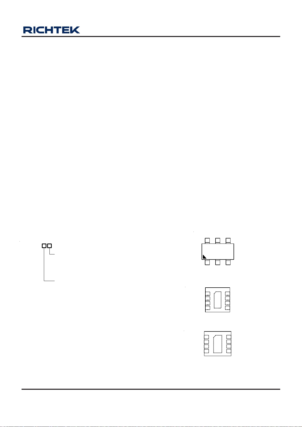
Pin Configurations
(TOP VIEW)
Ordering Information
RT9526
Package Type
E : SOT-23-6
QW : WDFN-8L 2x2 (W-Type)
QWA : WDFN-8L 2x3 (W-Type)
Lead Plating System
G : Green (Halogen Free and Pb Free)
Note :
Richtek products are :
` RoHS compliant and compatible with the current require-
ments of IPC/JEDEC J-STD-020.
` Suitable for use in SnPb or Pb-free soldering processes.
IMIN
CHG_SB GND VIN
SOT-23-6
1
VIN
2
PGB
ENB
3
4
CHG_SB
WDFN-8L 2x2
1
VIN
2
PGB
ENB
3
4
CHG_SB
WDFN-8L 2x3
ISET BATT
4
56
23
8
BATT
7
ISET
6
GND9IMIN
5
GND
8
BATT
7
ISET
6
GND
IMIN
9
5
GND
DS9526-01 April 2011 www.richtek.com
1
RT9526
Marking Information
RT9526GE RT9526GQW RT9526GQWA
EN= : Product Code
EX=DNN
DNN : Date Code
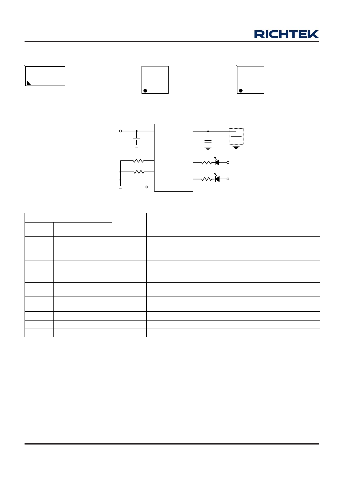
Typical Application Circuit
JJW 04W
JJ : Product Code
W : Date Code
04 : Product Code
W : Date Code
Adapter or USB
R
R
ISET
IMIN
VIN
C
IN
ISET
IMIN
GND
ENB
RT9526
CHG_SB
BATT
PGB
R1
R2
C
OUT
V
BATT
V
BATT
Function Pin Description
Pin No.
SOT-26-6
WDFN-8L 2x2 /
WDFN-8L 2x3
3 1 VIN Supply Voltag e Input. VIN can withstan d up to 28V input .
-- 2 PGB
1 3 CHG_SB
-- 4 ENB
2
9 (Exposed Pad)
5,
6 6 IMIN EOC Current Settin g Pin.
5 7 ISET Char ge Current Set Point.
4 8 BATT Battery Charge Curren t Output.
Pin Name Pin Function
Power Good Indicator. This pin connects to VIN with 10SL
N-MOSFET as power good c ondition.
Char ge Stat us Indicator Output (Open drain). Indicate low when
battery is charging; indicat e high when battery charging fini shed or
any fault happened.
Char ge En able (Active Lo w). Connect this pin with 2 00kΩ pull low
resistor.
GND
Ground. Th e exposed pad must be solde red to a large PCB and
conn ected to GND for maximum power dissipa tion.
DS9526-01 April 2011www.richtek.com
2
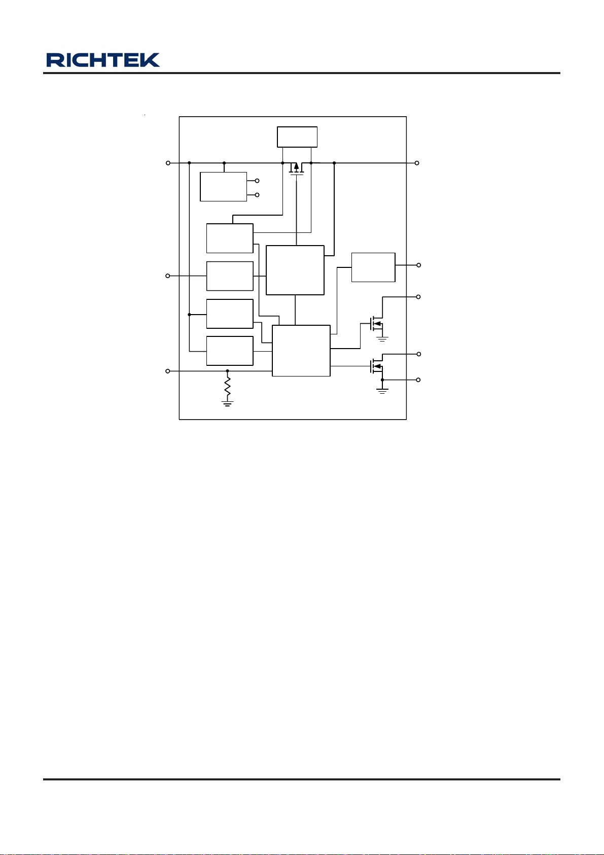
Function Block Diagram
RT9526
Switch
Well
VIN
ISET
ENB
BASE
Sleep
Mode
Current
Set Block
OVP
UVLO
200k
V
REF
I
BIAS
CC/CV/TR
Multi Loop
Controller
Logic
EOC Set
Block
BATT
IMIN
CHG_SB
PGB
GND
DS9526-01 April 2011 www.richtek.com
3
RT9526
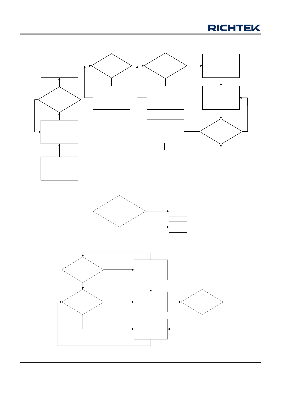
Flow Chart
Standby State
P-MOSFET = OFF
NO
V
< UVLO &
IN
V
< OVP &
IN
ENB = L
Power Off State
P-MOSFET = OFF
Any State or
> OVP or
V
IN
> UVLO or
V
IN
ENB = H
YES
V
- V
BATT
> V
OS
IN
NO
Sleep State
P-MOSFET = OFF
YES YES
BATT > 2.8V Soft-Start
NO
Pre_Charge
I
CHG_PRE
I
CHG_FAST, HG_SB = L
= (1/6) x
CV State
V
I
CHG =
= 4.2V
BATT
0A CHG_SB
= H
YES
Figure 1. Operation State Diagram for Charger function
Fast-Charge
I
CHG_FAST
R
SET
CHG_SB = L
V
BATT
= 150mA
= 29.4k
8 4.2V
≥
NO
VIN > UVLO
< OVP &
& V
IN
V
IN-VBATT
> V
OS
Figure 2. PGB State
ENB = L CHG _SB = H
YES
I
< I
IMIN
> 2.8V
&
CHG
V
BATT
NO
YES
NO
CHG_SB = H
CHG_SB = L
YES
NO
PGB = L
PGB = H
I
CHG
& V
YES
NO
< I
CHG_FAST
BATT
< 2.8V
Figure 3. CHG_SB State
DS9526-01 April 2011www.richtek.com
4
RT9526
Absolute Maximum Ratings (Note 1)
z Supply Voltage, VIN ------------------------------------------------------------------------------------------------------ −0.3V to 28V
z CHG_SB, PGB Pins ------------------------------------------------------------------------------------------------------ −0.3V to 7V
z Others ------------------------------------------------------------------------------------------------------------------------ −0.3V to 6V
z Power Dissipation, P
SOT-23-6 -------------------------------------------------------------------------------------------------------------------- 0.4W
WDFN-8L 2x2 -------------------------------------------------------------------------------------------------------------- 0.606W
WDFN-8L 2x3 -------------------------------------------------------------------------------------------------------------- 0.833W
z Package Thermal Resistance (Note 2)
SOT-23-6, θJA--------------------------------------------------------------------------------------------------------------- 250°C/W
WDFN-8L 2x2, θJA--------------------------------------------------------------------------------------------------------- 165°C/W
WDFN-8L 2x2, θJC--------------------------------------------------------------------------------------------------------- 8.2°C/W
WDFN-8L 2x3, θJA--------------------------------------------------------------------------------------------------------- 120°C/W
WDFN-8L 2x3, θJC--------------------------------------------------------------------------------------------------------- 8.2°C/W
z Lead Temperature (Soldering, 10 sec.)------------------------------------------------------------------------------- 260°C
z Junction Temperature ----------------------------------------------------------------------------------------------------- 150°C
z Storage Temperature Range -------------------------------------------------------------------------------------------- −65°C to 150°C
@ T
D
= 25°C
A
Recommended Operating Conditions (Note 3)
z Junction Temperature Range -------------------------------------------------------------------------------------------- −40°C to 125°C
z Ambient Temperature Range -------------------------------------------------------------------------------------------- −40°C to 85°C
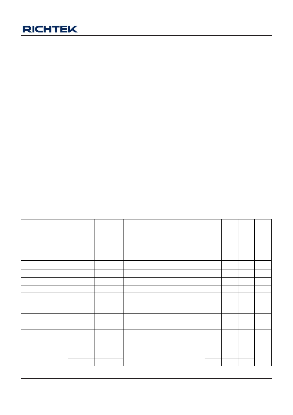
Electrical Characteristics
(V
= 4.5V, T
IN
VIN POR Rising Threshold
Voltage
VIN POR Falling Threshold
Voltage
VIN − V
VIN − V
VIN Standby Current V
BATT Sleep Leakage Current I
Battery Regulation Voltage V
VIN Power FET On-Resistance R
ISET Set Voltage (Fast Charge
Phase)
Charge Current Accuracy R
BATT Pre-Charge Threshold V
BATT Pre-Charge Threshold
Hysteresis
Pre-Charge Current I
ENB Input
Threshold Voltage
= 25°C unless otherwise specified)
A
Parameter Symbol Test Conditions Min Typ Max Unit
3.4 3.8 4.2 V
POR_H
3.1 3.5 3.9 V
POR_H
-- 90 150 mV
OS_H
10 50 -- mV
POR_L
= 4.5V -- 300 500 μA
BATT
-- 1 5 μA
4.158 4.2 4.242 V
REG
I
DS(ON)
-- 1.21 -- V
ISET
CHG_PRE
CHG_PRE
2.7 2.8 2.9 V
40 100 150 mV
= 0.5A -- 0.6 -- Ω
BATT
= 29.4kΩ 135 150 165 mA
ISET
12 16.7 21.3 %
V
= 4.2V to 24V
IL
IN
-- -- 0.4
V
VOS Ris ing V
BATT
VOS Falling V
BATT
Logic-High VIH 1.5 -- --
Logic-Low V
V
V
SLEEP
V
ΔV
CHG_PRE
To be continued
DS9526-01 April 2011 www.richtek.com
5

RT9526
Parameter Symbol Test Conditions Min Typ Max Unit
Thermal Regulation T
VIN Over Voltage Prote ction
Threshol d
VIN OVP Hysteresis ΔV
PGB Pull Down Voltage 5mA -- 200 -- mV
CHG_SB Pull Down Voltage 5mA -- 200 -- mV
EOC Current Setting I
EOC Rising Threshol d R
Note 1. Stresses listed as the above “Absolute Maximum Ratings” may cause permanent damage to the device. These are for
stress ratings. Functional operation of the device at these or any other conditions beyond those indicated in the operational
sections of the specifications is not implied. Exposure to absolute maximum rating conditions for extended periods may
remain possibility to affect device reliability.
Note 2. θ
Note 3. The device is not guaranteed to function outside its operating conditions.
is measured in natural convection at TA = 25°C on a low-effective thermal conductivity single-layer test board of
JA
JEDEC 51-3 thermal measurement standard. The measurement case position of θ
packages.
-- 115 -- °C
REG
V
10 11 13 V
OVP
-- 0.4 -- V
OVP
R
IMIN
= 137 kΩ 20 30 40 mA
IMIN
= 29.4kΩ 90 110 130 mA
IREF
is on the exposed pad of the
JC
DS9526-01 April 2011www.richtek.com
6

Typical Operating Characteristics
)
RT9526
Battery Current vs. Charging Time
0.20
0.18
0.16
0.14
0.12
0.10
0.08
0.06
Battery Current (A)
0.04
0.02
0.00
0 5000 10000 15000 20000 25000 30000 35000
Charging Time (s)
VIN = 5V, R
R
137kΩ
IMIN
=
= 29.4kΩ,
ISET
Battery Regulation Voltage vs. Charge Current
4.30
4.28
4.26
4.24
4.22
4.20
4.18
4.16
4.14
Battery Regulation Voltage (V) 1
4.12
4.10
0 100 200 300 400 500
Change Current (mA)
VIN = 5V
Battery Current vs. Charging Time
4.5
4.0
3.5
3.0
2.5
2.0
1.5
Battery Voltage (V)
1.0
0.5
0.0
0 5000 10000 15000 20000 25000 30000 35000
VIN = 5V, R
R
IMIN
=
ISET
137kΩ
Charging Time (s)
Charging Current vs. Input Voltage
155
150
V
= 3V
145
140
135
130
125
120
115
Charging Current (mA) 1
110
105
100
3.0 4.5 6.0 7.5 9.0 10.5
BATT
= 3.7V
V
BATT
Input Voltage (V)
R
ISET
= 29.4kΩ,
= 24.9Ω
Charge Current vs. Battery Voltage
500
VIN = 5V
450
400
350
300
250
200
150
Charge Current (mA
100
50
0
0.5 1.3 2.1 2.9 3.7 4.5
Battery Voltage (V)
R
R
R
ISET
ISET
ISET
= 9.1k
= 29.4k
= 9.1k
Battery Regulation Voltage vs . Input Voltage
4.4
4.2
4.0
3.8
3.6
3.4
Battery Regulation Voltage (V) 1
3.2
4567891011
Input Voltage (V)
I
BATT
= 20mA
DS9526-01 April 2011 www.richtek.com
7

RT9526
)
Charge Current vs. Temperature
180
160
140
120
100
80
60
Charge Current (mA
40
VIN = 5V, V
20
R
ISET
=
0
-50 -25 0 25 50 75 100 125
90
80
70
60
50
40
30
EOC Current (mA)
20
10
0
50 130 210 290 370 450
= 3.7V,
BATT
29.4kΩ
Temperature (°C)
EOC Current vs. R
(kΩ)
R
(kΩ)
IMIN
ISET
VIN = 5V, V
BATT
= 3.7V
Charge Current vs. R
1200
1100
1000
900
800
700
600
500
400
300
Charging Current (mA) 1
200
100
0
3 132333435363
R
ISET
VIN = 5V, V
kΩ
(kΩ)
ISET
BATT
= 3.7V
DS9526-01 April 2011www.richtek.com
8

Application Information
RT9526
The RT9526 is a fully integrated low cost single cell Li-ion
battery charger operable in Constant Current (CC) mode
or Constant Voltage (CV) mode. The CC mode current is
set with the external resistor, R
, and the CV mode
ISET
voltage is fixed at 4.2V. If the battery voltage is below a
typical 2.8V pre-charge threshold, the RT9526 charges
the battery with a trickle current until the battery voltage
rises above the pre-charge threshold. The RT9526 is
capable of being powered up from AC adapter and USB
(Universal Serial Bus) port inputs.
VIN Over Voltage Protection
The input voltage is monitored by the internal comparator.
The OVP threshold is set at 11V (typ.). When the input
voltage exceeds the threshold, the controller outputs a
logic signal to turn off the power P-MOSFET to prevent
high input voltage from damaging the electronics in the
handheld system. Nevertheless, an AC input voltage over
28V will still damage the RT9526. When the input over
voltage condition is removed, the controller will enable
the output again by running through soft-start.
Charger Enable Input
ENB is an active-low logic input to enable the charger.
Drive the ENB pin low or leave it floating to enable the
charger. This pin has a 200kΩ internal pull down resistor.
So when left floating, the input is equivalent to logic-low.
Drive this pin high to disable the charger.
Battery Charge Profile
The RT9526 charges a Li-ion battery under Constant
Current (CC) mode or Constant Voltage (CV) mode. The
constant current of ISET is set via the external resistor,
R
, and the constant voltage is fixed at 4.2V. If the battery
ISET
voltage is below a typical 2.8V pre-charge threshold, the
RT9526 charges the battery with a trickle current until
the battery voltage rises above the pre-charge threshold.
When the battery voltage reaches 4.2V, the charger enters
CV mode and regulates the battery voltage at 4.2V to
fully charge the battery without the risk of over charge.
CVCCTrickle
4.2V
I
CHG_FAST
2.8V
16.7 %
I
CHG_FAST
CHG_SB
Charge
Current
I
IMIN
CHG
Indication
Charge
Voltage
Figure 1. Typical Charge Profile
a. Battery Pre-Charge Current
During a charge cycle, if the battery voltage is below the
pre-charge threshold, the RT9526 applies a pre-charge
mode to the battery. This feature revives deeply discharged
cells and protects battery life. The internally determined
pre-charge rate of the RT9526 is 16.7% of the constant
charge current.
b. Battery Fast-Charge Current (CC Mode)
The RT9526 offers ISET pin to determine the fast-charge
current via an external resistor, R
, connected between
ISET
ISET and GND. The fast-charge current can be calculated
by the following equation :
V
I = K x (mA)
CHG_FAST ISET
K
= 3640; V
SET
SET
ISET
R
ISET
= 1.21 (typ.)
c. Battery Voltage Regulation (CV Mode)
The battery voltage regulation feedback is through the
BATT pin. The RT9526 monitors the battery voltage
between the BATT and GND pins. When battery voltage is
close to battery regulation voltage threshold, the voltage
regulation phase begins and the charging current begins
to taper down. When battery voltage is over battery
regulation voltage threshold and charge mode stops, the
RT9526 still monitors the battery voltage. Charge current
is resumed when the battery voltage falls under battery
regulation voltage threshold.
Sleep Mode
75 %
I
CHG_FAST
Time
The RT9526 enters sleep mode if both AC and USB are
removed from the input. This feature prevents draining the
battery during the absence of input supply.
DS9526-01 April 2011 www.richtek.com
9

RT9526
Power Good
This open-drain output pin is used to indicate the input
voltage status. The PGB output asserts low when
1. VIN > V
2. VIN
3. VIN < V
−−
− V
−−
POR
BATT
OVP
> V
OS
It can be used to drive an LED or communicate to the
host processor. Note that ON indicates the open-drain
transistor is turned on and LED is bright.
CHG_SB Indication
The CHG_SB pin is an open-drain output capable to at
least 10mA current when the charger starts to charge and
turns off when the EOC current is reached. The CHG_SB
signal is interfaced either with a micro processor GPIO or
an LED for indication.
End-Of-Charge Current (EOC)
Connect a resistor between the IMIN pin and GND to set
the EOC current. The EOC current level, I
programmable via the external resistor, R
IMIN,
, is
IMIN
as shown
in the following equation :
I =
IMIN
4148
R
IMIN
(mA)
Upon reaching the End-Of-Charge (EOC) current, the
charger indicates charge completion via the CHG_SB pin,
but the charger continues to output 4.2V voltage. Figure
1 shows the typical charge profile and the EOC/reset
event. The CHG_SB signal asserts low when the trickle
charge starts and changes to high at EOC. After EOC is
reached, the charge current has to rise above 75% of
I
CHG_FAST
before the CHG_SB signal is allowed to turn on
again. A current surge after EOC may occur due to a load
connected to the battery.
temperature falls below thermal regulation threshold
(115°C) by the hysteresis level. This feature prevents the
maximum power dissipation from exceeding typical design
conditions.
Selecting the Input and Output Capacitors
In most applications, a 1μF high frequency decoupling
capacitor placed in close proximity to the input is sufficient.
However, depending on the power supply characteristics
and cable length, it may be necessary to add an additional
10μF ceramic capacitor to the input. For the RT9526, a
small output capacitor is required for loop stability. A 1μF
ceramic capacitor placed between the BATT pin and GND
is typically sufficient.
Thermal Considerations
For recommended operating condition specifications of
the RT9526, the maximum junction temperature is 125°C
and TA is the ambient temperature. The junction to ambient
thermal resistance, θJA, is layout dependent. For
SOT-23-6 packages, the thermal resistance, θJA, is
250°C/W on a standard JEDEC 51-3 single-layer thermal
test board. For WDFN-8L 2x2 packages, the thermal
resistance, θJA, is 165°C/W on a standard JEDEC 51-3
single-layer thermal test board. For WDFN-8L 2x3
packages, the thermal resistance, θJA, is 120°C/W on a
standard JEDEC 51-3 single-layer thermal test board. The
maximum power dissipation at T
= 25°C can be calculated
A
by the following formula :
P
= (125°C − 25°C) / (250°C/W) = 0.400W for
D(MAX)
SOT-23-6 package
P
= (125°C − 25°C) / (165°C/W) = 0.606W for
D(MAX)
WDFN-8L 2x2 package
P
= (125°C − 25°C) / (120°C/W) = 0.833W for
D(MAX)
WDFN-8L 2x3 package
Temperature Regulation and Thermal Protection
In order to maximize charge rate, the RT9526 features a
junction temperature regulation loop. If the power
dissipation of the IC results in junction temperature greater
than the thermal regulation threshold (115°C), the RT9526
will cut back on the charge current and disconnect the
battery in order to maintain thermal regulation at around
115 °C. This operation continues until the junction
10
The maximum power dissipation depends on the operating
ambient temperature for fixed T
J (MAX)
and thermal
resistance, θJA. For the RT9526 packages, the derating
curves in Figure 2 allow the designer to see the effect of
rising ambient temperature on the maximum power
dissipation.
DS9526-01 April 2011www.richtek.com

RT9526
0.9
0.8
0.7
0.6
0.5
0.4
WDFN-8L 2x3
0.3
WDFN-8L 2x2
0.2
SOT-23-6
0.1
Maximum Power Dissipation (W) 1
0.0
0 25 50 75 100 125
Single-Layer PCB
Ambient Temperature (°C)
Figure 2. Derating Curve for RT9526 Package
Layout Consideration
The RT9526 is a fully integrated low cost single-cell Li-
ion battery charger ideal for portable applications. Careful
PCB layout is necessary. For best performance, place all
peripheral components as close to the IC as possible. A
short connection is highly recommended. The following
guidelines should be strictly followed when designing a
PCB layout for the RT9526.
` Input capacitor should be placed close to the IC and
connected to the ground plane. The trace of input on
the PCB should be placed far away from the sensitive
devices and shielded by the ground.
` The GND and exposed pad should be connected to a
strong ground plane for heat sinking and noise protection.
` The connection of R
should be isolated from other
ISET
noisy traces.
` Output capacitor should be placed close to the IC and
connected to the ground plane to reduce noise coupling.
BATT
BATT
R1
R2
C
should be placed near the
IN
IC to improve performance.
VIN BATT
C
OUT
C
IN
VIN
PGB
CHG_SB
ENB
1
2
3
4
8
BATT
7
ISET
6
GND9IMIN
5
GND
The GND plane should be connected to a strong
ground plane for heat sinking and noise protection.
Figure 3. PCB Layout Guide
The copper area connecting the
resistors of ISET and IMIN should
be minimized and kept far away
from noise sources.
R
ISET
R
IMIN
GND
DS9526-01 April 2011 www.richtek.com
11

RT9526
Outline Dimension
H
D
L
C
b
A
e
Dimensions In Millimeters Dimensions In Inches
Symbol
Min Max Min Max
A 0.889 1.295 0.031 0.051
A1 0.000 0.152 0.000 0.006
B 1.397 1.803 0.055 0.071
b 0.250 0.560 0.010 0.022
C 2.591 2.997 0.102 0.118
B
A1
D 2.692 3.099 0.106 0.122
e 0.838 1.041 0.033 0.041
H 0.080 0.254 0.003 0.010
L 0.300 0.610 0.012 0.024
SOT-23-6 Surface Mount Package
12
DS9526-01 April 2011www.richtek.com

RT9526
D
E
A
A3
A1
D2
L
E2
SEE DETAIL A
1
e
b
2
1
1
2
DETAIL A
Pin #1 ID and Tie Bar Mark Options
Note : The configuration of the Pin #1 identifier is optional,
but must be located within the zone indicated.
Dimensions In Millimeters Dimensions In Inches
Symbol
Min Max Min Max
A 0.700 0.800 0.028 0.031
A1 0.000 0.050 0.000 0.002
A3 0.175 0.250 0.007 0.010
b 0.200 0.300 0.008 0.012
D 1.950 2.050 0.077 0.081
D2 1.000 1.250 0.039 0.049
E 1.950 2.050 0.077 0.081
E2 0.400 0.650 0.016 0.026
e 0.500 0.020
L 0.300 0.400
W-Type 8L DFN 2x2 Package
0.012 0.016
DS9526-01 April 2011 www.richtek.com
13

RT9526
D
E
A
E2
A3
A1
D2
L
SEE DETAIL A
1
e
b
2
1
1
2
DETAIL A
Pin #1 ID and Tie Bar Mark Options
Note : The configuration of the Pin #1 identifier is optional,
but must be located within the zone indicated.
Dimensions In Millimeters Dimensions In Inches
Symbol
Min Max Min Max
A 0.700 0.800 0.028 0.031
A1 0.000 0.050 0.000 0.002
A3 0.175 0.250
b 0.200 0.300 0.008 0.012
D 1.900 2.100 0.075 0.083
D2 1.550 1.650 0.061 0.065
E 2.900 3.100 0.114 0.122
E2 1.650 1.750 0.065 0.069
e 0.500 0.020
L 0.350 0.450
Richtek Technology Corporation
Headquarter
5F, No. 20, Taiyuen Street, Chupei City
Hsinchu, Taiwan, R.O.C.
Tel: (8863)5526789 Fax: (8863)5526611
0.007 0.010
0.014 0.018
W-Type 8L DFN 2x3 Package
Richtek Technology Corporation
Taipei Office (Marketing)
5F, No. 95, Minchiuan Road, Hsintien City
Taipei County, Taiwan, R.O.C.
Tel: (8862)86672399 Fax: (8862)86672377
Email: marketing@richtek.com
Information that is provided by Richtek Technology Corporation is believed to be accurate and reliable. Richtek reserves the right to make any change in circuit design,
specification or other related things if necessary without notice at any time. No third party intellectual property infringement of the applications should be guaranteed
by users when integrating Richtek products into any application. No legal responsibility for any said applications is assumed by Richtek.
DS9526-01 April 2011www.richtek.com
14

 Loading...